Demonstration of high- TE-TM photonic crystal nanobeam cavities
Abstract
We experimentally demonstrate high Quality factor dual-polarized TE-TM photonic crystal nanobeam cavities. The free-standing nanobeams are fabricated in a 500 nm thick silicon layer, and are probed using both tapered optical fiber and free-space resonant scattering set-ups. We measure factors greater than for both TM and TE modes, and observe large fiber transmission drops (0.3 – 0.4) at the TM mode resonances.
Recently there has been significant interest in nanobeam photonic crystal microcavities. Although first proposed more than a decade ago Foresi et al. (1997), it was only recently shown that this architecture was capable of supporting ultra-high Q-factor cavities with dimensions on the order of a cubic wavelength in material Notomi et al. (2008); McCutcheon and Lončar (2008); Chan et al. (2009). Since then, there have been a host of new applications proposed and demonstrated, including optomechanical crystals Eichenfield et al. (2009), visible nanocavities Gong and Vučković (2010); Khan et al. (2010); Murshidy et al. (2010), low-power reconfigurable switches Frank et al. (2010), biosensors Falco et al. (2009); Wang et al. (2010), high transmission waveguides Quan et al. (2010); Zain et al. (2008) and lasers Halioua et al. (2010); Zhang et al. (2010). Recently, we showed theoretically that nanobeams could be engineered to have both TE and TM stopbands, provided the nanobeam is thick enough to support TM guided modes Zhang et al. (2009). High Q-factor cavity modes can be designed for both polarizations simultaneously by using an appropriate lattice tapering. By tuning the aspect ratio of the nanobeam (namely the height and width), the energy separation of the modes can be tuned. Dual-polarized nanocavities have the potential to open up new applications in chip-scale nonlinear optics. In particular, we have recently proposed such a system for single-photon frequency conversion in III-V materials McCutcheon et al. (2009); Burgess et al. (2009). These devices also raise the intriguing prospect of photonic crystal quantum cascade lasers Wakayama et al. (2008); Lončar et al. (2007), for which the radiation is TM-polarized.
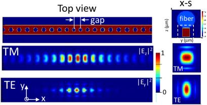
In this letter, we report the experimental observation of TE/TM dual-mode cavities in silicon. Our cavity design exploits the principles we (and others) have outlined in prior work Lalanne and Hugonin (2003); Sauvan et al. (2005); McCutcheon and Lončar (2008); Chan et al. (2009); Zhang et al. (2009); Deotare et al. (2009). We have shown that in principle, nanobeam cavities can be designed to have both TE and TM modes with Quality factors exceeding , but this requires a very thick structure with thickness:width:period ratio of 3:1:1 Zhang et al. (2009). Here, given our silicon device layer thickness of 500 nm and our operating wavelength near 1500 nm, the cavities were designed with TE and TM modes with Q factors of and 120,000, and mode volumes of 0.56 and 1.37, respectively. The nominal designs have nanobeam widths of 380-400 nm, hole pitch nm, radius , and a symmetric 6-period taper down to a pitch of in the center of the cavity. The TE and TM modes are separated by 50 nm, with the TE mode at higher energy. The field intensity profiles for the modes extracted from 3D finite-difference time-domain (FDTD) simulations are shown in Figure 1.
Because TM modes have the dominant electric field component oriented orthogonal to the device plane, they must be excited via evanescent Srinivasan et al. (2004) or end-fire waveguide coupling techniques Notomi et al. (2004). They cannot be readily probed from free-space McCutcheon et al. (2005), since like an electric dipole, they do not radiate parallel to the axis of the dipole moment. In order to probe our cavities, we use two complimentary techniques. Firstly, we employ a tapered fiber optical set-up. We pull an SMF-28 telecom fiber heated with a hydrogen torch to a diameter close to 1 m. The fiber is mounted in a U-shape, which self tensions the taper region and allows the fiber to be brought into close proximity with the sample surface. We then dimple the fiber by using a bare stripped fiber as a mold, and applying pressure to the narrowest part of the taper while heating the contact region Michael et al. (2007). The dimple, which is typically about 10 m in depth, as shown in Fig. 2, creates a local evanescent probe to the nanocavity of interest. The tapered fiber is spliced into an optical set-up, and its location with respect to the sample is precisely positioned using motorized stages with 50 nm encoder resolution (Surugu Seiki). The photodiode signal (Thorlabs Det010FC with a 1 k load resistor) is passed through a low noise Stanford pre-amplifier and low-pass filtered at 1 kHz before computer acquisition.
The second spectroscopy technique we use is a cross-polarized resonant scattering set-up, in which light incident from normal to the plane of the sample is strongly focused by a 100 objective and the reflected signal detected in the cross polarization McCutcheon et al. (2005). This method allows us to confirm the polarization of the modes detected by the tapered fiber, since it is only sensitive to the TE modes.
The cavities were fabricated with standard e-beam lithography and reactive ion etching methods, as described previously Deotare et al. (2009).
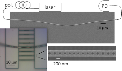
Figure 3 shows spectra from two different dual-polarization cavities. This represents, to our knowledge, the first experimental demonstration of high-, TE-TM nanocavities. The cavities are nominally identical except that the filling fraction of the air holes of cavity A (red) is slightly smaller compared to cavity B. These cavities are not actually fabricated according to the optimal design, but are intentionally detuned in order to lower the -factor of the TE mode and increase its visibility in the spectra. This is achieved by reducing the gap between the two central holes by 20 nm (see Fig. 1). We used a similar detuning method in previous work Deotare et al. (2009) to predictably shift the -factor and operating wavelength of our nanobeam cavities. Using SEM images of the fabricated structure, we perform 3D-FDTD simulations of cavity A, and predict = 27,000 and = 40,000.
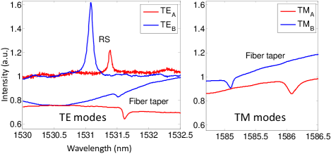
Measurements from both the fiber taper and resonant scattering set-ups are superimposed in the same graph. The TE modes near 1531 nm are revealed using both methods, and have -factors of 28,000, as determined by resonant scattering, which is a non-perturbative technique (i.e. it does not load the cavity). The TM modes near 1585 nm show signatures only in the fiber spectra, and have loaded -factors of 10,000. These measurements compare favorably with the 3D-FDTD results, considering the uncertainty in how exactly the fiber loads the cavity (the loaded TM -factor was simulated to be 20,000). The fiber transmission spectra are acquired by touching the fiber to the cavity (as visible in the optical image in Fig. 2), which was found to provide greater stability and repeatibility compared to evanescent coupling from the air. In the fiber data, the signatures of both the TE and TM modes are revealed as dips, since light which is “dropped” from the fiber into the cavity couples back into the fiber and interferes with the light transmitted directly through the fiber. On the other hand, in the resonant scattering spectra, free-space light incident from the normal direction can only resonantly scatter into the TE modes. No resonant features are seen at the TM wavelength. The TE modes are revealed as peaks on the non-resonant background (although both dips and Fano features Galli et al. (2009) are possible). The Lorentzian lineshapes are centered at the bare (unloaded) cavity resonance, and their widths give the unloaded -factors of the cavities. The fiber spectra are slightly red-shifted due to the perturbative effects of the silica fiber, and the exact positions of the resonances are dependent on how exactly the fiber contacts the particular cavity.
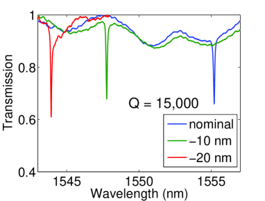
Having demonstrated high- TE-TM nanocavities, we now analyze the TM modes in greater detail. Although the strength of the fiber coupling to both the TE and TM modes is similar in Fig. 1, as measured by the depth of the transmission drop, in general we observe a greatly enhanced coupling to the TM modes compared to the TE modes in our fabricated structures. In Figure 4, we show a series of TM spectra from three cavities, which differ only in the spacing between the central two holes of the cavity. Each spectrum shows a large transmission drop on resonance. The cavity resonance blue-shifts as the central cavity gap is decreased, as expected. The -factor shows little variation over this range, and is approximately 15,000 for each of the cavities.
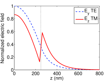
We attribute the greater fiber coupling of the TM modes to their greater overlap with the fiber mode. In Fig. 5, we plot the electric field strength for both TE and TM modes as a function of from the middle of the cavity. In the evanescent region (to the right of the dashed line), the TM E-field is twice the magnitude of the TE E-field. This is a consequence of the field boundary conditions. Since the electric field of the TM mode is dominantly perpendicular to the silicon/fiber interface, it must satisfy the boundary condition , where 1 denotes the silicon and 2 the fiber. By contrast, the TE mode fields are oriented parallel to the interface, and must therefore be continuous across the boundary i.e. . The on-resonance transmission can be estimated using coupled mode theory Spillane et al. (2003); Barclay et al. (2005), where the relevant coupling rates are extracted from FDTD simulations. The TM mode was designed to have a waveguide-limited -factor of 120,000. With the fiber touching the nanobeam, the loaded cavity -factor is 20,000, and the waveguide of the cavity is 180,000, from which we estimate a transmission of 0.7, a value consistent with our data (Fig. 4).
In conclusion, using a combination of fiber taper and resonant scattering spectroscopy, we have experimentally demonstrated high -factor, dual-polarized TE-TM photonic crystal nanobeam cavities in silicon. The modes are separated by 50 nm, and each has a -factor greater than . We observe large coupling of the TM modes in fiber taper transmission measurements, which we attribute to the significant evanescent tail of the TM mode above the cavity. We anticipate this phenomenon could be exploited for certain applications, such as bio-sensing Vollmer et al. (2002). More generally, we foresee TE-TM nanocavities playing an enabling role in many novel integrated applications, such as nonlinear wavelength conversion and quantum-cascade lasers.
References
- Foresi et al. (1997) J. S. Foresi, P. R. Villeneuve, J. Ferrara, E. R. Thoen, G. Steinmeyer, S. Fan, J. D. Joannopoulos, L. C. Kimerling, H. I. Smith, and E. P. Ippen, Nature 390, 143 (1997).
- Notomi et al. (2008) M. Notomi, E. Kuramochi, and H. Taniyama, Opt. Express 16, 11095 (2008).
- McCutcheon and Lončar (2008) M. W. McCutcheon and M. Lončar, Opt. Express 16, 19136 (2008).
- Chan et al. (2009) J. Chan, M. Eichenfield, R. Camacho, and O. Painter, Opt. Express 17, 3802 (2009).
- Eichenfield et al. (2009) M. Eichenfield, J. Chan, R. Camacho, K. J. Vahala, and O. Painter, Nature 462, 78 (2009).
- Gong and Vučković (2010) Y. Gong and J. Vučković, Appl. Phys. Lett. 96, 031107 (2010).
- Khan et al. (2010) M. Khan, T. M. Babinec, M. W. McCutcheon, P. B. Deotare, and M. Lončar, arxiv 1010.6287, (2010).
- Murshidy et al. (2010) M. M. Murshidy, A. M. Adawi, P. W. Fry, and D. G. Lidzey, Appl. Phys. Lett. 97, 153303 (2010).
- Frank et al. (2010) I. W. Frank, P. B. Deotare, M. W. McCutcheon, and M. Lončar, Opt. Express 18, 8705 (2010).
- Falco et al. (2009) A. D. Falco, L. O’Faolain, and T. F. Krauss, Appl. Phys. Lett. 94, 063503 (2009).
- Wang et al. (2010) B. Wang, M. A. Dundar, R. Notzel, F. Karouta, S. He, and R. W. van der Heijden, Appl. Phys. Lett. 97, 151105 (2010).
- Quan et al. (2010) Q. Quan, P. B. Deotare, and M. Lončar, Appl. Phys. Lett. 96, 203102 (2010).
- Zain et al. (2008) A. R. M. Zain, M. Gnan, H. M. H. Chong, M. Sorel, and R. M. D. L. Rue, IEEE Photon. Technol. Lett. 20, 6 (2008).
- Halioua et al. (2010) Y. Halioua, A. Bazin, P. Monnier, T. J. Karle, I. Sagnes, G. Roelkens, D. V. Thourhout, F. Raineri, and R. Raj, J. Opt. Soc. Am. B 27, 2146 (2010).
- Zhang et al. (2010) Y. Zhang, M. Khan, Y. Huang, J. H. Ryou, P. B. Deotare, R. Dupuis, and M. Lončar, Appl. Phys. Lett. 97, 051104 (2010).
- Zhang et al. (2009) Y. Zhang, M. W. McCutcheon, I. B. Burgess, and M. Lončar, Opt. Lett. 34, 2694 (2009).
- McCutcheon et al. (2009) M. W. McCutcheon, D. E. Chang, Y. Zhang, M. D. Lukin, and M. Lončar, Opt. Express 17, 22689 (2009).
- Burgess et al. (2009) I. B. Burgess, Y. Zhang, M. W. McCutcheon, A. W. Rodriguez, J. Bravo-Abad, S. G. Johnson, and M. Lončar, Opt. Express 17, 20099 (2009).
- Wakayama et al. (2008) Y. Wakayama, A. Tandaechanurat, S. Iwamoto, and Y. Arakawa, Opt. Express 16, 21321 (2008).
- Lončar et al. (2007) M. Lončar, B. G. Lee, L. Diehl, M. A. Belkin, F. Capasso, M. Giovannini, J. Faist, and E. Gini, Opt. Express 15, 4499 (2007).
- Lalanne and Hugonin (2003) P. Lalanne and J. P. Hugonin, IEEE J. Quantum Electron. 39, 1430 (2003).
- Sauvan et al. (2005) C. Sauvan, G. Lecamp, P. Lalanne, and J. Hugonin, Opt. Express 13, 245 (2005).
- Deotare et al. (2009) P. B. Deotare, M. W. McCutcheon, I. W. Frank, M. Khan, and M. Loncar, Appl. Phys. Lett. 94, 121106 (2009).
- Srinivasan et al. (2004) K. Srinivasan, P. E. Barclay, M. Borselli, and O. Painter, Phys. Rev. B 70, 081306(R) (2004).
- Notomi et al. (2004) M. Notomi, A. Shinya, S. Mitsugu, E. Kuramochi, and H.-Y. Ryu, Opt. Express 12, 1551 (2004).
- McCutcheon et al. (2005) M. W. McCutcheon, G. W. Rieger, I. W. Cheung, J. F. Young, D. Dalacu, S. Frédérick, P. J. Poole, G. C. Aers, and R. L. Williams, Appl. Phys. Lett. 87, 221110 (2005).
- Michael et al. (2007) C. P. Michael, M. Borselli, T. J. Johnson, C. Chrystal, and O. Painter, Opt. Express 15, 4745 (2007).
- Galli et al. (2009) M. Galli, S. L. Portalupi, M. Belotti, L. C. Andreani, L. O¢Faolain, and T. F. Krauss, Appl. Phys. Lett. 94, 071101 (2009).
- Spillane et al. (2003) S. M. Spillane, T. J. Kippenberg, O. J. Painter, and K. J. Vahala, Phys. Rev. Lett. 91, 043902 (2003).
- Barclay et al. (2005) P. E. Barclay, K. Srinivasan, and O. Painter, Opt. Express 13, 801 (2005).
- Vollmer et al. (2002) F. Vollmer, D. Braun, A. Libchaber, M. Khoshsima, I. Teraoka, and S. Arnold, Appl. Phys. Lett. 80, 4057 (2002).