Direct observation of band-gap closure for a semiconducting carbon nanotube in a large parallel magnetic field
Abstract
We have investigated the magnetoconductance of semiconducting carbon nanotubes (CNTs) in pulsed, parallel magnetic fields up to 60 T, and report the direct observation of the predicted band-gap closure and the reopening of the gap under variation of the applied magnetic field. We also highlight the important influence of mechanical strain on the magnetoconductance of the CNTs.
pacs:
73.63.Fg, 75.47.-m, 73.23.AdCarbon nanotubes (CNTs) are attractive building blocks for nanoelectronic devices. While electronic properties of CNTs are determined to be either metallic or semiconducting once they are grown, a magnetic field parallel to the tube axis provides an elegant way to tune the band structure of a CNT after its growth Ajiki . The origin of the sensitivity to lies in the contribution of the Aharonov-Bohm (AB) phase to the orbital phases picked up by electrons encircling the perimeter of the tube. The AB phase tunes the periodic boundary condition along the tube circumference and results in a -periodic modulation of the band gap Ajiki ; Coskun ; Lassagne , where is the flux quantum. Recently, significant drops in conductance were induced by for initially metallic CNTs Lassagne ; Fedorov2 ; Jhang as the energy gap of metallic CNTs linearly opens with magnetic flux for /2. For semiconducting CNTs, theory predicts that the initial energy gap linearly decreases with to close the gap at /3, and reopens reaching a local maximum at /2. The gap then closes again at /3 and recovers its original value at Ajiki ; Charlier . However, as actual magnetic fields equivalent to are about 5000 and 50 T for CNTs with diameters of 1 and 10 nm, respectively, the AB effect of semiconducting CNTs has only been partially investigated for Minot ; Zaric ; Fedorov3 , and the direct observation of the predicted semiconductor-to-metal transition at /3 has so far remained elusive. Moreover, while CNTs of 5.5 nm are necessary to achieve /3 within the accessible fields of about 60 T in a specialized pulsed-magnet lab, the magnetoconductance (MC) in thick CNTs is often strongly affected by disorder and quantum interference effects Stojetz ; Fedorov , making it difficult to solely identify the AB effects on the band structure.
In this Letter, we report a magneto-transport study on a clean semiconducting CNT performed in pulsed magnetic fields of up to 60 T. The MC of the tube showed a clear manifestation of the AB effect on the band structure when located near the charge neutrality point (CNP). The conductance changes with by more than 100 times showing a peak, then a dip close to /2 before approaching the second peak. The position of the peak is shifted from the expected /3, which can be explained by the effect of mechanical strain originating from the tube bending.
Our experiments have been performed on devices made of individual CVD-grown CNTs on Si/SiO2/Si3N4 substrates Kong . The heavily -doped Si was used as a back gate and the thickness of the insulating layer was 350 nm. Pd (50 nm) electrodes were defined on top of the tubes by e-beam lithography. The distance between two Pd electrodes was 500 nm. The dc two-probe magnetoconductance was studied in pulsed magnetic fields, applied parallel to the tube axis. The data presented here were obtained from a CNT ( 8 nm) smoothly bent with a nearly constant curvature on the substrate as shown in Fig. 1(b).
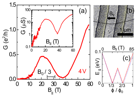
Fig. 1(a) displays the MC trace of the semiconducting CNT, measured at 3.1 K. The conductance at zero field (0) is greatly suppressed as the Fermi energy is located near the CNP by applying a gate voltage V. With the application of , () exponentially increases by two orders of magnitude to recover the level of one conductance quantum () until it reaches a peak at 22 T. The conductance then drops back to a minimum around 37 T, before increasing towards the expected second peak. Although the second peak was not reachable in our experiment, the negative curvature of the MC curve near 60 T, seen in the inset of Fig. 1(a), indicates that the second peak is located not far above 60 T. We also notice (). For comparison, we calculated the energy gap in for a (95,15) CNT (with similar to our tube) presented in Fig. 1(c); the large consecutive change in the conductance agrees in general with the band-gap modulation due to the AB effect. The conductance peak at 22 T and the minimum at 37 T can be attributed to the band-gap closure at /3 and a local maximum at /2, respectively. The observation, (), results from the fact that (/2) = (0). However, we note two experimental observations not explained within the simple model: 1) The height of the first peak is smaller than that of the second peak. 2) If 22 T corresponds to the band-gap closure at /3, then the second peak should already appear at 44 T. Also, the diameter nm, determined from the atomic force microscope (AFM), rather suggests 24.5 /3 31.5 T.
In the following, we show that the shifted positions of the MC peaks can be explained by the effect of mechanical strain in CNTs. The structural deformation, such as the strain and tube bending, plays an important role in the electronic structure of CNTs Yang ; Chibotaru ; Minot2 ; Huang . Previous works Yang ; Minot2 ; Huang showed that the band gap of the CNTs changes by 100 meV per 1% strain, due to the shift of the and Dirac points under the strain. This change of the band gap () is independent of diameter, whereas for semiconducting CNTs. Therefore, the effect of strain becomes more important for larger diameter tubes.
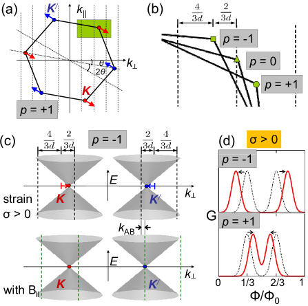
Fig. 2 illustrates the shift of the and Dirac points under uniaxial strain, and the resulting effects on the positions of the MC peaks. The shift of the -points depends on the uniaxial strain and the chiral angle , and is given by Yang
| (1) |
where for the and Dirac points, is the C-C bond length, and being the Poisson ratio. It is displayed in Fig. 2 for the case of tensile strain ( 0).
Due to the shift of the -points under 0, the positions of the gap closure at /3 and at /3 are also shifted either closer (for ) or away from each other (for ) depending on the type of the semiconducting CNT (Fig. 2(d)). Here such that the chiral indices satisfy with being an integer. For the case of compressive strain ( 0), the effects are opposite with the type . Supposing the type of our tube as and 0 (or and 0), we can explain the positions of the MC peaks in our data. For tubes with and 0, the first peak at /3 is shifted to the left, and the second peak at /3 to the right by the amount of . Assuming the shifted peaks at 22 T and 60 T, a simple calculation calculation leads to 82 T and 5 T. This value of corresponds to 1.8 10-3 from Eq. (LABEL:eq:k), supposing 0.2 Sanchez . Therefore, even small axial strain for zigzag tubes () would explain the shift of MC peaks observed in our data equation . Without the strain-induced shift, the model suggests the MC peaks occur at 27 and 55 T with the -periodicity of 82 T. This value of , equivalent to nm, now shows a good agreement with the diameter of our tube obtained from AFM. Note that the diameter shrinkage due to the strain ( nm) is negligible. The existence of a small strain is likely in our device, as our tube was mechanically deformed during the growth on the SiO2 substrates [Fig. 1(b)] thermal .
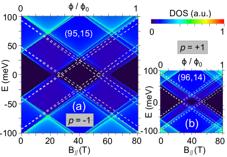
Taking the (95,15) tube ( 8.1 nm and ) as a model CNT with , we calculated the density of states (DOS) in a parallel magnetic field at strain. For comparison, we present the DOS of a (96,14) tube, which has almost the same and , but with . The DOS was calculated from the dispersion relation, with momenta close to the Fermi points modified according to Eq. (LABEL:eq:k). We used periodic boundary conditions in the axial direction, suitable for very long nanotubes. Displayed in Fig. 3, the dashed lines indicate the positions of the band edges without strain. At zero field, the axial strain either reduces (for ) or increases (for ) the band gap of the CNTs, as demonstrated by previous experiments Minot2 ; Huang . With the application of , the band edges evolve, reflecting the orbital and Zeeman splitting. While the band gap is closed for both tubes at 27 and 54 T without strain, the positions of the band-gap closure shift under strain, resulting in the gap closure at 22 and 58 T for the (95,15) tube, and at 32 and 48 T for the (96,14) CNT. The relation (0) becomes under strain (0) (for ) [or (0) (for )].
The DOS calculated for the (95,15) tube at strain shows in general good agreement with the positions of the MC peaks for our tube. However, the calculation neglects the tube bending and the coupling between different shells Kwon ; Marganska of multi-walled CNTs, assuming the charge transport mainly through the outermost shell. Also, quantum interference effects in the Fabry-Perot regime, such as the AB beating effect Cao are ignored. Therefore, we cannot expect to explain all features of the measured MC within our simple model.
If the charge transport also occurs through the inner shell, the second peak at 60 T can be due to the band-gap closure (at /3) from the inner shell, while the first peak at 22 T originates from the outer shell of the tube. However, corresponding of 5.4 and 9 nm for the inner and the outer shell, calculated from this model, differ significantly from the known inter-shell distance in multi-walled CNTs ( 0.34 nm) Iijima .
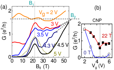
In order to confirm our interpretation of the data, we investigated the evolution of the versus . In Fig. 4(a), MC traces at 3.5 K are displayed mainly for the hole side of the CNP, where the CNT/Pd interface is most transparent Interface . At 0, the hole conductance at 2 V is high, almost 2, and decreases rapidly as the Fermi energy is tuned towards the CNP ( 4.5 V). Whereas the MC traces for 2 V stay flat except for small fluctuations, a large conductance modulation appears only close to the CNP.
Fig. 4(b) presents the gate characteristics at 0 and 22 T, deduced from the MC traces in Fig. 4(a). at 22 T shows that a small gap still remains at , whereas the AB effect predicts a complete gap closure at /3. On the other hand, the extrapolated MC curves converge at 45 T [Fig. 4(a)], indicating a complete gap closure for the assumed second peak around 60 T. The remaining small gap at is responsible for the smaller height of the first peak in Fig. 1(a), compared to that of the second peak.
The Zeeman effect splits antiparallel spin states and reduces the band gap by 0.1 [meV/T] , affecting the -periodic modulation of the band gap Coskun ; Jiang as shown in Fig. 1(c). Including the Zeeman effect, the small gap observed at is closed when the Zeeman contribution becomes larger than at higher . The complete gap closure for the assumed second peak around 60 T suggests the size of 6 meV, since corresponds to 6 meV at 60 T.
Turning our attention to the origin of at , the tube bending can mix the states between the quantized lines of allowed and open a gap for metallic CNTs Chibotaru . Therefore, a bending-induced gap , competing with , is present at /3 and at /3 for curved CNTs, partly contributing to . However, Chibotaru , with an estimated bending diameter of 10 m, is too small ( 1 meV) to explain the . On the other hand, the inter-shell interaction can also lead to a gap, for example, when the symmetry is lowered by disorienting one shell axis with respect to the other Kwon . Therefore, the observed at for our tube might originate from the inter-shell interaction, apart from the bending-induced gap.
Finally, we discuss the possible effect of spin-orbit coupling Kuemmeth ; Ando on the MC of semiconducting CNTs. The spin splitting induced by spin-orbit coupling results in a peculiar double-peak MC structure for a chiral metallic CNT, as reported in our previous work Jhang . For semiconducting CNTs, the MC peak at /3 does not split into two, as the Zeeman contribution at /3 () is much larger than the spin-orbit energy splitting () SO .
In conclusion, our experiment clearly shows that a semiconducting CNT can be converted into a metallic one with the application of large , providing a consistent confirmation of the AB effect on the band structure of semiconducting CNTs. In addition, we reveal that the position of the band-gap closure at /3 can be tuned by mechanical strain. Combined control of both the strain and the AB effect may open up new possibilities for magneto-electronic and magneto-optical CNT devices.
We acknowledge B. Witkamp and H. van der Zant for help in the growth of CNTs. This research was supported by the Deutsche Forschungsgemeinschaft within GRK 1570 and SFB 689 and by EuroMagNET under the EU contract No. 228043.
References
- (1) H. Ajiki and T. Ando, J. Phys. Soc. Jpn. 62, 1255 (1993).
- (2) U. C. Coskun et al., Science 304, 1132 (2004).
- (3) B. Lassagne et al., Phys. Rev. Lett. 98, 176802 (2007).
- (4) G. Fedorov et al., Nano Lett. 7, 960 (2007).
- (5) S. H. Jhang et al., Phys. Rev. B 82, 041404 (2010).
- (6) J.-C. Charlier, X. Blase, and S. Roche, Rev. Mod. Phys. 79, 677 (2007).
- (7) E. D. Minot et al., Nature (London) 428, 536 (2004).
- (8) S. Zaric et al., Science 304, 1129 (2004).
- (9) G. Fedorov et al., Appl. Phys. Lett. 96, 132101 (2010).
- (10) G. Fedorov et al., Phys. Rev. Lett. 94, 066801 (2005).
- (11) B. Stojetz et al., Phys. Rev. Lett. 94, 186802 (2005).
- (12) J. Kong et al., Nature (London) 395, 878 (1998).
- (13) L. Yang and J. Han, Phys. Rev. Lett. 85, 154 (2000).
- (14) L. F. Chibotaru, S. A. Bovin, and A. Ceulemans, Phys. Rev. B 66, 161401 (2002).
- (15) E. D. Minot et al., Phys. Rev. Lett. 90, 156401 (2003).
- (16) M. Huang et al., Phys. Rev. Lett. 100, 136803 (2008).
- (17) /3 22 T and 2/3 60 T.
- (18) D. Sánchez-Portal et al., Phys. Rev. B 59, 12678 (1999).
- (19) Eq. (LABEL:eq:k) was confirmed by experiment Huang with an additional prefactor of 0.57. This would result in twice as large strain to explain the shift of the MC peaks in our data.
- (20) As our tube is fixed to electrodes on the substrate, different thermal-expansion coefficients between Si and CNT can also play a role. Using K-1 and K-1 at room temperature Huang , a rough estimate leads to , with K, consistent with our data.
- (21) Y.-K. Kwon and D. Tománek, Phys. Rev. B 58, 16001 (1998).
- (22) M. Margańska, S. Wang, and M. Grifoni, New J. Phys. 11, 033031 (2009).
- (23) J. Cao et al., Phys. Rev. Lett. 93, 216803 (2004).
- (24) S. Iijima, Nature (London) 354, 56 (1991).
- (25) Due to the difference in the work functions of the contact metal Pd and CNT, Schottky barriers at the CNT/metal interface become important for the electron side of the CNP. Therefore, the electron and the hole transmission probabilities are not symmetric with respect to the CNP owing to the difference in the contact properties; the conductance on the electron side is considerably lower as shown in Fig. 4(b). Hence, in the manuscript we focus on the hole side of the CNP, where we have the most transparent contacts at the CNT/Pd interface.
- (26) J. Jiang, J. Dong, and D. Y. Xing, Phys. Rev. B 62, 13209 (2000).
- (27) T. Ando, J. Phys. Soc. Jpn. 69, 1757 (2000).
- (28) F. Kuemmeth et al., Nature (London) 452, 448 (2008).
- (29) For our tube with of 8 nm, 3 meV and 0.2 meV at /3.