Probing La0.7Sr0.3MnO3 multilayers via spin wave resonances
Abstract
La0.7Sr0.3MnO3/BiFeO3 and La0.7Sr0.3MnO3/PbZr20Ti80O3 epitaxial heterostructures have been grown on SrTiO3 substrates. Spin wave resonances are used to study interface properties of the ferromagnetic La0.7Sr0.3MnO3. We find that the addition of the BiFeO3 or PbZr20Ti80O3 causes out-of-plane surface pinning of the La0.7Sr0.3MnO3. We are able to place new limits on the exchange constant D of La0.7Sr0.3MnO3 grown on these substrates and confirm the presence of uniaxial and biaxial anisotropies caused by the SrTiO3 substrate.
I Introduction
The promise of electrically and magnetically tunable tunnel junctions for use in both spin valves and four state memory devices(springerlink:10.1007/s11434-008-0275-8, ; majumdar:122114, ; PhysRevB.75.245324, ), is an exciting prospect. La1-xSrxMnO3/BiFeO3(LSMO/BFO) multilayers are proposed for spin valve devices, as LSMO has demonstrated good spin filtering properties(nature_LSMO, ) and BFO is a room temperature multiferroic which could, in principle, provide an electrically tunable exchange biased film(doi:10.1021/nl801391m, ; adma.200502622, ; Nature-Mat-BFO-Bias, ). Both of these materials are perovskite based structures and have small lattice mismatch when grown on a suitable substrate. Practically, it is important to understand how the magnetization of LSMO films is affected when epitaxially joined to a ferroelectric. Enhancement of uniaxial anisotropies, development of unidirectional anisotropies, surface pinning from the interface and changes to other micromagnetic parameters are all important characteristics with respect to tunnel junction performance. Though most of these properties have been explored in single layer LSMO(4837696, ; Gomes20101174, ; PhysRevB.78.094413, ; PhysRevB.76.184413, ; PhysRevB.73.054406, ; suzuki:140, ; lofland:1947, ; Dho200723, ; 5026792, ), the effects of ferroelectric overlayers can be important and have begun to be studiedPhysRevLett.104.167203 ; thiele:262502 . In this paper we examine pinning of dynamic magnetization using spin wave measurements. A new result is our measure for the spin wave exchange constant D. To the best of the authors knowledge, only four other measurements of D have been carried out so far(PhysRevB.76.184413, ; PhysRevB.53.14285, ; vasiliu-doloc:7342, ; Moudden1997276, ), and only one study which utilises standing spin wave modes for determination of D(PhysRevB.76.184413, ). We also use standing spin wave resonances to measure anisotropies caused by both the ferroelectric overlayer and growth of LSMO on a single crystal substrate.
II Standing Spin Wave Modes
A powerful technique to probe magnetic conditions at buried interfaces is through spin wave resonances(PhysRevB.38.6847, ; PhysRevB.58.8605, ; Kittel_Formula, ; Classic_Kittel_FMR, ; Spin_Wave_Resonance_First_Experiment, ).
The structure of standing spin wave modes contains detailed information about bulk magnetic properties, such as gyromagnetic ratio and exchange constant D, and also provides information about interfacial pinning of the magnetization vector.
The ferromagnetic resonance frequency for out-of-plane magnetized thin films is
| (1) |
where , is the precession frequency, is the gyromagnetic ratio, is the externally applied field , is the demagnetizing field due to the out-of-plane alignment of spins, is any bulk out-of-plane anisotropy field and is the exchange energy of the standing spin wave mode. Measurement of multiple modes allows determination of and . Separation of and , is possible when the fundamental resonance mode frequency (FMR mode) and the first exchange mode (FEX mode) are measured. Due to the shorter wavelength and much higher energy density of the FEX mode, any changes in wavelength due to surface pinning strongly affect the frequency gap between the FEX and FMR modes.
Subtraction of the effective field data of the FEX mode , from the FMR mode gives us a measure of the strength of pinning and the exchange constant. By rotating the film in-plane and taking angular measurements, the angular variation of pinning and bulk anisotropies may be determined.
Angular dependence of spin wave frequencies for in plane magnetization can be used to measure magnetocrystalline anisotropies. The Kittel formula describing resonance conditions for the magnetization oriented in-plane is(Kittel_Formula, )
| (2) | |||||
Here is the in-plane bulk anisotropy and refers to the wave vector of standing wave modes with magnetization aligned in plane. We make distinct and which need not in general be the same depending upon pinning conditions at the film interface. Also included is an angular dependence which denotes the magnetization direction with respect to some arbitrary in-plane film direction.
The paper is structured as follows. We first describe sample growth and characterization, and the ferromagnetic resonance experiment. FMR results are presented along with a discussion of bulk and surface anisotropies. We conclude with results for the exchange constant D of La1-xSrxMnO3 films.
III Sample growth and characterization
A series of films comprising epitaxial La0.7Sr0.3MnO3 (LSMO) were grown on single crystal (100) orientated SrTiO3 (STO) substrates, with the addition of either an epitaxial BiFeO3 (BFO) or PbZr20Ti80O3 (PZT) capping layer. As a comparision, a thick polycrystalline LSMO film was grown on MgAl2O4. All films were grown via Pulsed Laser Deposition (PLD) with a KrF excimer laser at 248 nm with laser fluency of 2 Jcm-2. The STO substrates were sourced from Shinkosa Co. LTD Japan with a manufacturers claim of less then 0.3o miscut, and arrived pre-etched to provide a TiO2 terminated surface. All substrates were sonicated in isopropyl alcohol to remove organic contaminates before use. The deposition chamber base pressure was better than 5.010-7 Torr before the sample was heated to deposition temperature and a partial oxygen pressure was introduced. LSMO films were deposited at 700 degrees Celsius with an oxygen partial pressure of 100 mT, repetition rate of 10Hz, laser fluence of 1.8 J cm-2 and were cooled under 300 Torr O2 at 5 degrees per minute. BFO films were deposited at 700 degrees Celsius with an oxygen partial pressure of 5 mT, repetition rate of 20Hz, laser fluence of 1.6 Jcm-2 and were cooled under 220 Torr O2 at 5 degrees per minute. PZT films were deposited at 550 degrees Celcius with an oxygen partial presssure of 100 mT, repetition rate of 3 Hz, laser fluence of 1.6 Jcm-2 and were cooled under 700 Torr O2 at 5 degrees per minute. The growth rate of LSMO, BFO and PZT were 0.002 nm/pulse, 0.004 nm/pulse and 0.002 nm/pulse respectively. LSMO and BFO phase purity was confirmed via standard X-Ray diffraction on a Philips Xpert Pro MRD system. An example is shown in Fig. (1).
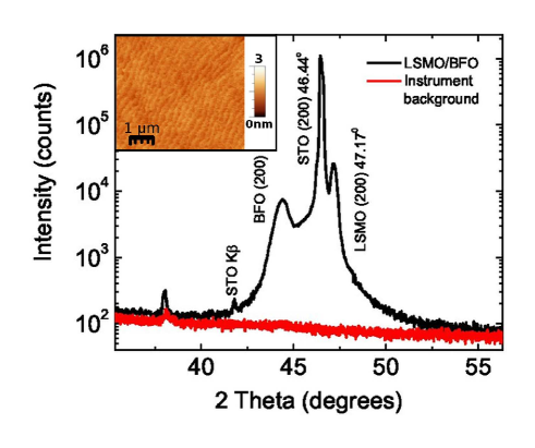
The LSMO thickness was calibrated via X-Ray reflectivity measurements on a Philips Xpert Pro MRD system. The BFO thickness was calibrated via TEM analysis, as published in(doi:10.1002/adfm.201000265, ). Our samples exhibit low surface roughness, less then 2.6Å rms, indicating smooth growth as shown in Fig.(1).
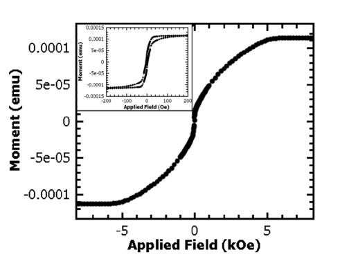
A step pattern is seen which exists in the underlying STO substrates and is preserved throughout the LSMO epitaxial growth. In-plane and out-of-plane SQUID magnetometry was performed, and from this data (seen in Fig.(2)) was determined to be 0.50.05 T.
IV Ferromagnetic Resonance
The FMR characterisation was done using a Vector Network Analyser (VNA) and Field-Modulated (FM) FMR setups. The VNA-FMR is used to obtain S21 parameters from field swept measurements as discussed in (screening-published, ). It consists of a Danphysik power supply to drive the electromagnets, and an Agilent N5230 PNA-L vector network analyser operating in a 1-20GHz frequency range. The FM-FMR setup uses the VNA as the microwave source, and an SRS SR850 lock-in amplifier and HP 33120A function generator to drive the field modulated measurements. In both cases a 0.3mm microstrip waveguide was used as the microwave antenna source as shown in Fig.(3). The sample is placed with the film in direct contact with the microstrip.
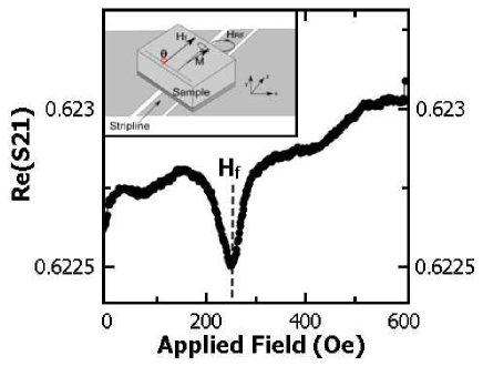
The in-plane FMR procedure for extracting resonance conditions is as follows. The frequency is constant, and an external magnetic field is swept while the S21 transmission coefficients are measured. This procedure is repeated for several different frequencies. An example result is shown in Fig.(3).
V FMR Results and discussion
Only the FMR resonance was observed for the in-plane configuration. Lack of FEX mode absorption may correspond to weak surface pinning in the plane of the film. If surface pinning is weak, then the FEX mode has a symmetric magnetisation profile across the film thickness, producing no net dipole moment to couple to(Classic_Kittel_FMR, ). In this case, only a non-uniform driving field, caused for example by eddy currents in a conducting sample, can drive resonance(kostylev-2008, ; screening_unpublished, ; PhysRev.97.1558, ; khivintsev:023907, ; PhysRev.118.658, ). Due to the low conductivity of LSMO compared to Permalloy, we do not expect significant non-uniformity of driving field across the sample thicknesses studied. Hence the FEX mode visibility should originate primarily from intrinsic surface pinning.
Magnetocrystalline anisotropies can be determined for angular measurements in-plane, as noted above. The results for an angular study of just the FMR mode is displayed in Fig.(4).
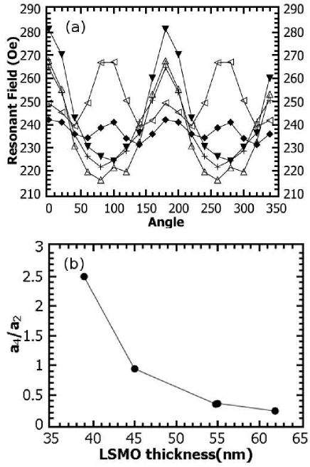
The type of anisotropy seems to be dependent on the film thickness. Biaxial and uniaxial anisotropies can be identified with the thinnest LSMO film having a biaxial character and the thickest LSMO films having a uniaxial character. There is also the case of the intermediate 45nm LSMO film which displays an unequal mixing of both uniaxial and biaxial character. Quantitative information on the form of the angular anisotropies can be obtained by fitting to:
| (3) |
where HR is the resonant applied field, is the film angle with respect to the applied field, a2 is a uniaxial anisotropy term, a4 is a biaxial anisotropy term. The are phase shifts of the anisotropies with respect to the 0o measurement direction. Examining the ratio as a function of LSMO thickness reveals a trend as shown in Fig.(4). This indicates that the uniaxial anisotropy dominates over the biaxial anisotropy as the LSMO thickness increases. Furthermore, this effect is related to the LSMO and substrate, as it does not appear to be correlated with the capping layer.
Previous studies have noted both uniaxial and biaxial anisotropies present in STO/LSMO films, with the biaxial anisotropy originating from the cubic symmetries of epitaxial LSMO grown on (001) STO and the uniaxial anisotropies originating from physical steps on the STO surface(4817880, ; suzuki:140, ; APL-1.1578711, ; arxiv:1005.0553v1, ). It was reported that the in-plane four-fold and two-fold anisotropies are bulk in origin and not strongly related to interface pinning.
It should be noted however that both anisotropies are established during the growth process. In particular, because we measure a strong uniaxial anisotropy for quite thick (60nm) LSMO films, it would seem unlikely that step defects(PRB.1999.58.18, ; PhysRevB.49.15084, ; NeelReducedSymmetry, ), could explain these observations. The fact that this uniaxial anisotropy is dominant in thick LSMO films suggest that some kind of bulk structure established firstly at the step boundary, and then propagates as the LSMO grows(APL-1.1578711, ).
Each of the curves in Fig.(4) has a different dc-offset, which does not depend on LSMO thickness in a systematic way. The most likely explanation for this is either differences in saturation magnetisation or pinning and out of plane anisotropy originating at the ferroelectric interface. Without the additional FEX modes for the in-plane data it is difficult to assess the contribution made by the ferroelectric layer to in-plane surface anisotropies.
FMR and FEX modes were seen in out-of-plane configuration measurements for some films. The lack of an FEX mode for in-plane measurements, and its presence in out-of-plane resonance measurements, indicate that surface pinning is most effective in the out-of-plane direction. When the surface pinning originates from an easy axis out-of-plane anisotropy, it has been shown that both dynamic components of magnetisation are pinned when the out-of-plane configuration, but that only one component is pinned when the magnetisation is in-planeSalansky-book . As shown in Fig.(5) there is a strong FMR mode which is present in all films and a FEX mode is observed in some films.
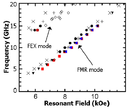
By fitting straight lines to the data in Fig.(5) we may extract and from Eq.(1). A comparison of these parameters for the different films is shown in Tab.(1).
| Sample | ||||
|---|---|---|---|---|
| STO/LSMO(30nm) | 2.79 | 2.79 | -4425 | -956 |
| STO/LSMO(38.9nm) | 2.67 | 2.67 | -4624 | -973 |
| STO/LSMO(61.9nm) | 2.83 | - | -4891 | - |
| STO/LSMO(55nm)/BFO(18nm) | 2.63 | - | -4442 | - |
| STO/LSMO(54.8nm)/BFO(24nm) | 2.64 | 2.64 | -4423 | -437 |
| STO/LSMO(45nm)/PZT(20nm) | 2.63 | 2.63 | -4089 | 176 |
The gyromagnetic ratio is extracted from the slope of the data given in Fig.(5). is measured by the intercept with for out-of-plane measurements. While the monolayer LSMO shows a net decrease in with thickness, indicating a reduction in out-of-plane anisotropies, the addition of a ferroelectric layer significantly changes . It should be noted that the PZT seems to much more strongly affect the magnetic parameters then BFO.
VI Spin Wave Stiffness
We now discuss determination of D. We define the gap between effective fields for the two modes as:
Eq.(VI) does not contain contributions from , as this contributes equally to both and .
Tab.(2) lists the results of this gap for films in which the FEX mode was observed, and also for estimates of what these values should be assuming no interface pinning and the literature value of Dlit= 1.796510-17T m2(or in the units for exchange stiffness D 104meV Å). We note that the spin wave constant D used in the Kittel equation has units T m2 and spin wave stiffness Dstiffness possesses units J m2(PhysRevB.76.184413, ). Converting between the two uses the following:
| Heff (experimental) | Heff (no pinning, Dlit) | |
|---|---|---|
| LSMO(30nm) | 3651 | 1970 |
| LSMO(38.9nm) | 3496 | 1171 |
| LSMO(45nm)/PZT(20nm) | 4265 | 875 |
| LSMO(54.8nm)/BFO(24nm) | 3986 | 590 |
| no pinning | max single sided pinning | max double sided pinning | |
|---|---|---|---|
| Dlit | 1171 | 2343 | 3515 |
| 1.49 Dlit | 1745 | 3491 | 5237 |
| 2.98 Dlit | 3491 | 6983 | 10475 |
We see immediately that there is a large discrepancy between the observed and predicted . It is not possible from observations of two standing spin wave modes to identify separately pinning at each interface. We thus consider two extreme situations: complete pinning at the ferroelectric interface only (single sided pinning) and complete pinning at both interfaces (double sided pinning)111We note that if complete pinning does occur at both interfaces, then the first exchange mode becomes symmetric and will not be excited by a uniform driving field. In our experiment, only the conductivity would cause a non-uniform driving field, and this effect is estimated to be quite weak for LSMO. Hence a first exchange mode which experiences double sided pinning would be extremely difficult to detect. In our estimation of the theoretical range of D we neglect this fact.. D values deduced from measured gaps in 38.9nm LSMO films for extreme pinning conditions are given in Tab.(3). The case where Dlit accounts for can only occur for double sided pinning. In the case where extreme single sided magnetisation pinning exists, an exchange constant value of at least 1.49 Dlit is needed. Finally the case where can be explained without any interface pinning is only possible for 2.98 Dlit. Most likely, a combination of both a larger D combined with some pinning from both interfaces would account for the D value we find. In addition, there is clearly a much greater gap for the films with a capping ferroelectric, especially for the PZT capped film. This indicates a significant out-of-plane interface pinning which originates from the ferroelectric layer.
VII Summary
Ferromagnetic resonance was used as a sensitive probe of both in-plane and out-of-plane anisotropies in multilayer LSMO/BFO and LSMO/PZT films. We have shown that some interface pinning must be playing a role in magnetisation dynamics. Interestingly, BFO seems to have little influence on the magnetisation of LSMO. We see no evidence of exchange bias(doi:10.1021/nl801391m, ; adma.200502622, ), though this may be because of the relatively thick LSMO layer dominating the magnetisation dynamics. The fast growth rate of BFO in comparison to(doi:10.1021/nl801391m, ) may also be an important factor in growing suitable BFO to couple to the ferromagnet. Electric fields were applied across the BFO layer and resonance experiments were carried out, but no shifts in FMR resonances were observed. From our data, it is quite difficult to extract separate pinning effects at each interface. However, a lower bound for D can be set given various assumptions about pinning at the interface. We find that complete pinning at both interfaces gives D for our films the same as literature Dlit.
Uniaxial and biaxial in-plane anisotropies appear to be unrelated to the capping ferroelectric layer are observed, and there may exist a thickness of LSMO about which a transition between anisotropies might take place. Our data indicates that the uniaxial contribution to anisotropy relative to the biaxial component increases as the ferromagnet thickness increases, for LSMO films grown on STO(100), unlike that found for LSMO grown on other substrates(4837696, ).
Acknowledgements.
We acknowledge the support of the ARC, University of Western Australia, DEST and the DIISR Australia India Strategic Research Fund ST020078.References
- (1) Z. Shi, C. Wang, X. Liu, and C. Nan, Chinese Sci. Bull. 53, 2135 (2008)
- (2) S. Majumdar, R. Laiho, P. Laukkanen, I. J. Väyrynen, H. S. Majumdar, and R. Österbacka, Appl. Phys. Lett. 89, 122114 (2006)
- (3) F. J. Wang, C. G. Yang, Z. V. Vardeny, and X. G. Li, Phys. Rev. B 75, 245324 (Jun 2007)
- (4) J.-H. Park, E. Vescovo, H. J. Kim, C. Kwon, R. Ramesh, and T. Venkatesan, Nature (London) 392, 794 (1998)
- (5) L. W. Martin, Y.-H. Chu, M. B. Holcomb, M. Huijben, P. Yu, S.-J. Han, D. Lee, S. X. Wang, and R. Ramesh, Nano Lett. 8, 2050 (2008)
- (6) J. Dho, X. Qi, H. Kim, J. MacManus-Driscoll, and M. Blamire, Adv. Mater. 18, 1445 (2006)
- (7) S. M. Wu, S. A. Cybart, P. Yu, M. D. Rossell, J. X. Zhang, R. Ramesh, and R. C. Dynes, Nat. Mater. 9, 756 (2010)
- (8) H. Nishikawa, E. Houwman, H. Boschker, M. Mathews, D. H. A. Blank, and G. Rijnders, Appl. Phys. Lett. 94, 042502 (jan 2009)
- (9) I. Gomes, B. Almeida, A. Lopes, J. Araújo, J. Barbosa, and J. Mendes, J. Magn. Magn. Mater 322, 1174 (2010), ISSN 0304-8853
- (10) M. Huijben, L. W. Martin, Y.-H. Chu, M. B. Holcomb, P. Yu, G. Rijnders, D. H. A. Blank, and R. Ramesh, Phys. Rev. B 78, 094413 (Sep 2008)
- (11) M. Golosovsky, P. Monod, P. K. Muduli, and R. C. Budhani, Phys. Rev. B 76, 184413 (Nov 2007)
- (12) A. A. Sidorenko, G. Allodi, R. De Renzi, G. Balestrino, and M. Angeloni, Phys. Rev. B 73, 054406 (Feb 2006)
- (13) Y. Suzuki, H. Y. Hwang, S.-W. Cheong, and R. B. van Dover, Appl. Phys. Lett. 71, 140 (1997)
- (14) S. E. Lofland, S. M. Bhagat, Q. Q. Shu, M. C. Robson, and R. Ramesh, Appl. Phys. Lett. 75, 1947 (1999)
- (15) J. Dho and N. Hur, J. Magn. Magn. Mater. 318, 23 (2007), ISSN 0304-8853
- (16) L. B. Steren, M. Sirena, and J. Guimpel, J. Appl. Phys. 87, 6755 (may. 2000)
- (17) M. Ziese, I. Vrejoiu, E. Pippel, P. Esquinazi, D. Hesse, C. Etz, J. Henk, A. Ernst, I. V. Maznichenko, W. Hergert, and I. Mertig, Phys. Rev. Lett. 104, 167203 (Apr 2010)
- (18) C. Thiele, K. Dörr, S. Fähler, L. Schultz, D. C. Meyer, A. A. Levin, and P. Paufler, Applied Physics Letters 87, 262502 (2005)
- (19) M. C. Martin, G. Shirane, Y. Endoh, K. Hirota, Y. Moritomo, and Y. Tokura, Phys. Rev. B 53, 14285 (Jun 1996)
- (20) L. Vasiliu-Doloc, J. W. Lynn, Y. M. Mukovskii, A. A. Arsenov, and D. A. Shulyatev, J. Appl. Phys. 83, 7342 (1998)
- (21) A. H. Moudden, L. Vasiliu-Doloc, L. Pinsard, and A. Revcolevschi, Physica B 241-243, 276 (1997)
- (22) W. Stoecklein, S. S. P. Parkin, and J. C. Scott, Phys. Rev. B 38, 6847 (1988)
- (23) R. D. McMichael, M. D. Stiles, P. J. Chen, and W. F. Egelhoff, Phys. Rev. B 58, 8605 (1998)
- (24) C. Kittel, Introduction to Solid State Physics, 8th ed. (John Wiley & Sons, Inc, 2005)
- (25) C. Kittel, Phys. Rev. 110 (1958)
- (26) J. M. H. Seavey and P. Tannenwald, Phys. Rev. Lett. 1, 168 (1958)
- (27) M. Hambe, A. Petraru, N. A. Pertsev, P. Munrow, V. Nagarajan, and H. Kohlstedt, Adv. Func. Mater. 20, 2436 (2010)
- (28) K. J. Kennewell, M. Kostylev, N. Ross, R. Magaraggia, R. L. Stamps, M. Ali, A. A. Stashkevich, D. Greig, and B. J. Hickey, J. Appl. Phys. 108 (2010)
- (29) M. Kostylev, Journal of Applied Physics 106, 043903 (2009)
- (30) K. J. Kennewell, M. Kostylev, M. Ali, A. A. Stashkevich, R. Magaraggia, D. Greig, B. J. Hickey, and R. L. Stamps, arXiv: 1001.1837v1(2010)
- (31) W. S. Ament and G. T. Rado, Phys. Rev. 97, 1558 (1955)
- (32) Y. V. Khivintsev, L. Reisman, J. Lovejoy, R. Adam, C. M. Schneider, R. E. Camley, and Z. J. Celinski, J. Appl. Phys. 108, 023907 (2010)
- (33) P. Pincus, Phys. Rev. 118, 658 (1960)
- (34) M. Mathews, F. M. Postma, J. C. Lodder, R. Jansen, G. Rijnders, and D. H. A. Blank, Appl. Phys. Lett. 87, 242507 (dec. 2005)
- (35) Z. H. Wang, G. Cristiani, and H. U. Habermeier, Appl. Phys. Lett 82, 3731 (2003)
- (36) P. Perna, E. Jiménez, F. J. Teran, L. Méchin, N. Mikuszeit, J. Camarero, and R. Miranda, arXiv:1005.0553v1(2001)
- (37) R. Arias and D. L. Mills, Phys. Rev. B. 59, 11871 (1999)
- (38) D. S. Chuang, C. A. Ballentine, and R. C. O’Handley, Phys. Rev. B 49, 15084 (Jun 1994)
- (39) L. Néel, J. Phys. Radium 15, 225 (1954)
- (40) N. Salansky and M. Erukhimov, Physical properties and application of magnetic films (Moscow: Nauka, 1975)
- (41) We note that if complete pinning does occur at both interfaces, then the first exchange mode becomes symmetric and will not be excited by a uniform driving field. In our experiment, only the conductivity would cause a non-uniform driving field, and this effect is estimated to be quite weak for LSMO. Hence a first exchange mode which experiences double sided pinning would be extremely difficult to detect. In our estimation of the theoretical range of D we neglect this fact.