Publishing information:
T. Kühn and G. S. Paraoanu, Electronic and thermal sequential transport in metallic and superconducting two-junction arrays, in Trends in nanophysics: theory, experiment, technology, edited by V. Barsan and A. Aldea, Engineering Materials Series, Springer-Verlag, Berlin (ISBN: 978-3-642-12069-5), pp. 99-131 (2010).
DOI: 10.1007/978-3-642-12070-1_5
Electronic and thermal sequential transport in metallic and superconducting two-junction arrays
Abstract
The description of transport phenomena in devices consisting of arrays of tunnel junctions, and the experimental confirmation of these predictions is one of the great successes of mesoscopic physics. The aim of this paper is to give a self-consistent review of sequential transport processes in such devices, based on the so-called ”orthodox” model. We calculate numerically the current-voltage (–) curves, the conductance versus bias voltage (–) curves, and the associated thermal transport in symmetric and asymmetric two-junction arrays such as Coulomb-blockade thermometers (CBTs), superconducting-insulator-normal-insulator-superconducting (SINIS) structures, and superconducting single-electron transistors (SETs). We investigate the behavior of these systems at the singularity-matching bias points, the dependence of microrefrigeration effects on the charging energy of the island, and the effect of a finite superconducting gap on Coulomb-blockade thermometry.
I Introduction
Quasiparticle transport processes across metallic junctions play a fundamental role in the functioning of many devices used nowadays in mesoscopic physics. One such device is the single electron transistor (SET), invented and fabricated almost two decades ago averinlikharev , which has found remarkable applications as ultrasensitive charge detector electrometer and as amplifier operating at the quantum limit quantumamplifier . In the emerging field of quantum computing the superconducting SET has been proposed and used as a quantum bit qubit . With advancements in lithography techniques, this device can be fully suspended suset , thus providing a new avenue for nanoelectromechanics. Similar devices are currently used (in practice arrays with several junctions turn out to provide a larger signal-to-noise ratio) as Coulomb blockade (CBT) primary thermometers cbt . Also, superconducting double-junction systems with appropriate bias can be operated as microcoolers microcoolers . The functioning of these three classes of devices is based on the interplay between two out of the three relevant energy scales: the superconducting gap, the charging energy, and the temperature.
For example, in the case of microcoolers, the temperature and the gap are finite, and the charging energy is typically zero. A natural question to raise is then what happens if the charging energy is no longer negligible, for example if one wishes to miniaturize further these devices. In contradistinction, for CBTs the charging energy and the temperature are important, and the superconducting gap is a nuisance. A solution is to suppress the gap by using external magnetic fields, an idea which makes these temperature sensors more bulky and risky to use near magnetic-field sensitive components. Therefore, understanding the corrections introduced by the superconducting gap could provide an interesting alternative route, although, with present technology, the level of control required of the gap value could be very difficult to achieve. Finally, electrometers and superconducting SETs are operated at low temperatures, with the charging energy and the gap being dominant. However, large charging energies are not always easy to obtain for some materials due to technological limitations, while achieving effective very low electronic temperatures is limited by various nonequilibrium processes.
In this article we present a unified treatment of these three devices by solving the transport problem in the most general case, when all three energy scales are present. Our goal is to give an eye guidance for the experimentalist working in the field, showing what are the main characteristics visible in the –s and –s, resulting from sequential tunneling. Both the electrical and the thermal transport are calculated in the framework of a generalized so-called ”orthodox” theory, which includes the superconducting gap. For completeness, we offer a self-consistent review of this theory, which has become nowadays the standard model for describing sequential quasiparticle transport processes in these devices. We ignore Josephson effects which, for the purpose of this analysis just add certain well-known features at certain values of the bias (the Josephson supercurrent at zero bias and the Josephson-quasiparticle (JQP) peak at for symmetric SETs) to the characteristic. Higher-order tunneling phenomena such as Andreev reflections and cotunneling are neglected as well (the former is visible only for junctions with high transparencies, which is not our case, the latter is a small, second-order transport effect across the island). Also the effect of the environment is not discussed here, since it depends on the specifics of the sample (for example the coupling capacitances of the electrodes). But even stripped down to the essentials of sequential tunneling, the physics of these devices is complex enough to justify a careful analysis, as we attempt below. We present in detail the theory and the numerical methods that can be used to characterize these devices. Also, a lot of interest exists nowadays in the study of hybrid structures – in which the electrodes and the island are made from different materials, thus having different superconducting gaps. Various technologies have been developed to fabricate single-electron transistors with superconducting materials other than Al, most notably with Nb which has a much larger gap us . We extend our analysis also to such hybrid SETs.
This paper is organized in the following way: besides the introductory part, there are two main sections, Section II and Section III, followed by closing remarks in Section IV. Section II discusses tunneling of electrons from one superconductor into another through an insulating barrier. Here we show how to calculate the currents that flow through the junction by using the Fermi golden rule (Subsection II.1), and we give a comprehensive presentation of the numerical methods used to calculate the integrals over the density of states and Fermi functions which appear naturally in this theory (Subsection II.2). In Section III we use these results to describe transport phenomena in two-junction devices. We assume a quasi-equilibrium situation (electron distribution described by a Fermi function with a certain effective temperature) for both the island and the leads. We start with a presentation of the master equation in Subsection III.1. A first application of this formalism is described in Subsection III.2, where we analyze the effect of a finite superconducting gap for the functioning of Coulomb-blockade thermometers. Then we discuss the effect of a nonzero charging energy for superconductor-insulator-normal metal-insulator-superconductor (SINIS) structures (Subsection III.3) – which normally have a negligible charging energy. After that, in Subsection III.4, we consider the case of superconducting single-electron transistors with either identical materials in the leads and island (symmetric SET) or with an island with a gap different from that of the electrodes (asymmetric SET). The effect of the gate in such transistors is further investigated in Subsection III.5. We end this section with a calculation of expected cooling effects in such structures (Subsection III.6). We delegate some of the calculations of integrals in Appendix A, and of expansions in Appendix B.
II Transport in single tunnel junctions
Standard lithographic techniques enable the fabrication of junctions with almost any geometrical characteristics down to the linewidth of the respective system. When using scanning-electron microscopes, the typical linewidths obtained are of the order of 20 nm and even below. More advanced methods, such as focused ion beam lithography, have started to be used recently. The metals are evaporated in an ultra-high vacuum evaporator, using the shadow evaporation technique. This technique consists of evaporation through a mask realized in the resist, at different angles, so that some lines would overlap in a certain region, thus defining the area of the junction. In between two evaporations, the sample is oxidized (typically aluminum oxide), a process which results in the formation of the insulating barrier.
In this section, we assume that the area of the junction thus formed is large enough so that capacitive effects can be neglected (Coulomb-blockade effects are discussed in the next section). This allows us to concentrate on tunneling effects only. The only energy scales relevant here will then be the temperature and the tunneling matrix element.
II.1 General theory of tunneling
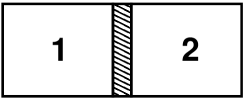
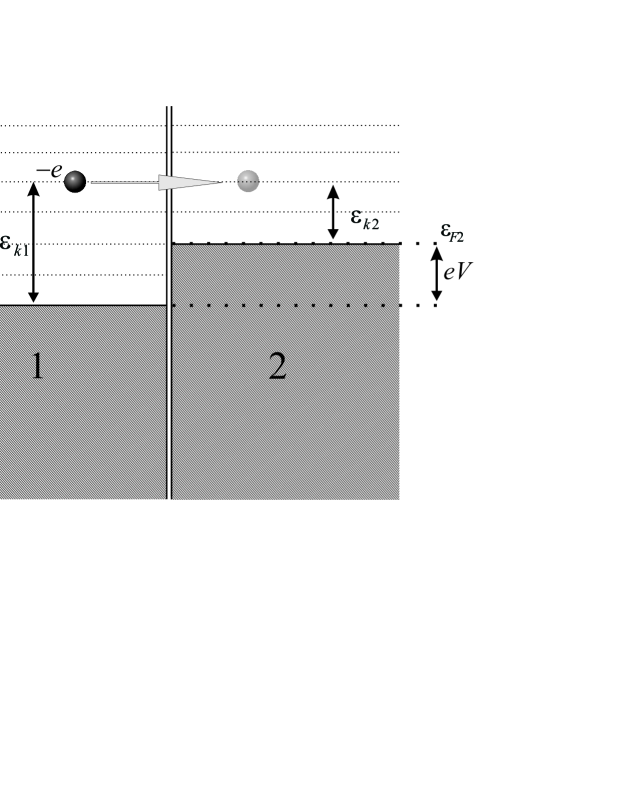
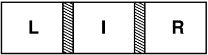
Consider the case of two conductors (leads) that are connected through a thin insulating barrier. The setup is illustrated in Fig. 1. This creates effectively a potential barrier between the ”left” and ”right” electrodes: however electrons can still tunnel from one side to another via the tunneling effect. The total many-body Hamiltonian of the system comprises then two parts: one is the Hamiltonian corresponding to the left and right electrodes (which can be either the free-electron Hamiltonian in the case of metals, or the BCS Hamiltonian in the case of superconductors), the other is the tunneling Hamiltonian. This Hamiltonian was first introduced by Bardeen bardeen :
| (1) |
where and are the momentum indices corresponding to the left and right electrodes, and is the spin index (conserved under tunneling); and are creation and annihilation operators for fermions. It is then straightforward to calculate the probability per unit time (the tunneling rate) that an electron residing in the left electrode would tunnel from a state (of energy , where is the Fermi level of the left electrode) to a state (of energy , where is the Fermi energy of the right electrode), by a direct application of the Fermi Golden rule,
| (2) |
where are the Fermi functions corresponding to the states , is the density of states (without the spin degrees of freedom) at , and is the energy difference between the states and , . The energy difference does not depend on the state or since it is due to electrical potentials such as an external battery or to the charging of the island (as we will see below in the case of single-electron transistor) which produce a difference in the Fermi energies of the two metals, , meaning that , and thus ensuring that the total energy is conserved under tunneling.
Replacing now the sum over states with a continuous integral, we can find the total tunneling rate from left to right by integrating , weighted with the density of states ,
| (3) |
The last form of the equation, using the Dirac delta function (in no danger of confusion with the of ), reflects indeed the conservation of energy: electrons of energy can get only to states , if they acquire an energy gain of with respect to their Fermi levels. Inelastic processes are allowed in a more general formulation, which includes the degrees of freedom of the environment, in which case is replaced by the so-called -function ingold . Also, the factor of 2 appearing in front of the integral comes from summation over the spin index. The rate of tunneling from the right electrode to the left one, , is calculated in a similar way. The difference between these quantities represents the net current of charges flowing through the junction, therefore the net electrical current is
| (4) |
We then get, using the expressions Eq. (3) and Eq. (2),
| (5) |
where we conveniently change all the momentum indices to continuous-energies functions. To make progress with Eq. (5), a few assumptions are needed. First of all, already embedded in the theory above is the idea that tunneling does not significantly change the Fermi distribution function. Nonequilibrium processes however can play an important role, requiring a more involved treatment using Green’s functions review . Next, the Fermi energy in most metals is of the order of a few s; this is large when compared to the typical bias voltages at which such junctions are studied. Then, in the case of metals, the density of states can be considered constant around the corresponding Fermi energies , and . For superconducting electrodes this assumption does not hold: the density of states is divergent around the gap, and, as we will see below, this has significant effects. It is however possible (see below) to isolate the divergent part of the density of states as an adimensional quantity which, when multiplied with the normal-metal density of states around the Fermi level would give an approximate but still correct superconducting density of states. Finally, the tunneling matrix element can also be taken as energy-independent, . With these assumptions, the integral over energies in Eq. (3) can be performed (see ingold ; schon and Appendix A), using the generally useful result
| (6) |
to give for the tunneling rates
| (7) |
For example, at zero temperature we find for and for . The value of the current does not depend however on temperature. From Eq. (7) and Eq. (4) we find a linear dependence in for the current
| (8) |
If , as it is in the case of a voltage-biased single junction (see Fig. 1), we immediately recognize Ohm’s law from Eq. (8), ; with the quanta of resistance defined as we get
| (9) |
The theory presented above looks very reasonable until one realizes – horribile dictu! – that in fact the result Eq. (9) predicts a rather absurd scaling of electrical resistance with the dimensions of the sample. Let us look at the densities of state. The three-dimensional density of states per volume (with spin states excluded) can be calculated using the standard text-book expression
| (10) |
The Fermi energy for metals is of the order of a few eV: for example, eV, eV, eV, eV. At eV we obtain for example ; the Fermi wavelength at eV is = 0.37 nm.
The problem now is that in order to find we have to multiply the density of states per volume with the volume of the electrodes. This is of course absurd, as the inverse of resistance should be linear in the junction’s surface and not depend on the volume of the electrodes. The solution to this conundrum stems from the idea that the summation in Eq. (3) has to be done under the restriction that transversal momentum is conserved (specular transmission): thus the correct densities of states that appear further have to be densities of states at fixed transversal momentum harrison . Also the assumption of energy-independence of the tunneling matrix element does not necessarily hold true for most practical junctions. A complete theory of tunneling that takes into consideration all these special features has been developed over the years simons . However, with the trick of absorbing the density of states into the tunneling resistance, the theory described above is still useful, describing correctly the voltage dependence of the current. As we will see below, the theory can be extended to the case of superconductors. Similar tunneling theories can be constructed for scanning tunneling microscopy, where the densities of state refer to the tip of the instrument and to the surface of the sample hofer . Also, the same structure has been successfully applied to systems such as trapped atoms, where the tunneling can be realized by using RF fields coupled to internal hyperfine states of the atoms paivi . In this case, is given by the detuning of the RF field with respect to the atomic frequency, and the tunneling matrix element is truly constant (given by the coupling amplitude of the field with the atoms). In this situation, the current of particles between two hyperfine states depends indeed on the volume of the samples, as it should be, since the field penetrates the sample completely and tunneling between the internal states occurs not only at some interface but in the whole volume. This case also has its specifics however: the momentum (and not only the energy) is conserved.
In the case of superconductors, the theory proceeds as above, but the density of states used has to be replaced by that given by the BCS theory. It turns out that this density of states consists of a factor which is the same as for metals, which gets multiplied by a divergent part near the gap. It is then natural to introduce a normalized density of states , which would take the value 1 for metals,
| (11) |
and will be a function
| (12) |
for BCS superconductors ( is the superconducting gap and is the Heavyside function).
Summarizing all the discussion above, we can write the tunneling probability, including both the metallic and superconducting case, as
| (13a) | |||||
| (13b) | |||||
with being the normalized density of states of the electrodes, as introduced above. Furthermore, given the tunneling probabilities of Eq. (13), the current through a single superconducting tunnel junction without charging effects is given as
| (14) |
II.2 Numerical methods
For the discussion in this subsection we use the shorthand notation . Now Eq. (13) can be solved analytically for some limiting cases, as we have already seen for the case of normal metal electrodes, or can be expressed as a combination of special functions. For example, in the case of a SIN junction, the calculation at zero temperature is straightforward. From Eq. (13b) we get
| (15) |
which can be seen for example in Figure 2 bottom left (the additional spike appearing there at is a singularity-matching peak discussed below; it shows up because the temperature is finite). In this figure, and .
In practice however, in the general case of non-identical superconductors and finite temperature, it has to be solved numerically, and, due to the singularities in the BCS density of states, the numerical treatment of Eq. (13) is somewhat challenging (see Fig. 2). We therefore want to discuss the numerical problems arising from these divergencies and possible ways to solve them in a bit more detail.
Inserting Eq. (12) into Eq. (13b), one can easily see that the expression for the electron tunneling probability splits into four separate integrals,
| (16) |
where the integrals are given by
| (17a) | |||||
| (17b) | |||||
| (17c) | |||||
| (17d) | |||||
The limits of these integrals are set by the -functions in the BCS density of states. The function is then
| (18) |
Due to the singularities in the BCS density of states, the function is singular in each of the finite limits of the integrals .
In most cases these singularities can be handled easily enough with the help of a simple integral transformation. As the function behaves qualitatively like , where is smooth on the interval of integration, we can substitute and we are left with an integral which is numerically easily handled:
| (19) |
However, for certain values of , the singularities of the densities of states of the first and second lead will coincide, leading to two logarithmic divergences known as singularity matching peaks at and two finite steps at the quasiparticle threshold .
Singularity-matching peaks: We will first discuss the singularity matching peaks, which are described by the integrals and . When is close to , the integration results can become very inaccurate, and the transformation done in Eq. (19) will not help to solve the problem. We can however separate the singularity from the integral by partial integration, leaving us with a finite and easily integrable rest term. We note that the general form of integrals and is
| (20) |
As is proportional to the Fermi distribution, and all its derivatives exponentially tend to zero for large values of . Furthermore, is analytic on the interval . Using partial integration, we obtain
| (21) |
with the big advantage that the singularity itself is described by an explicit expression rather than an integral. The integral in the second term is finite and easily computed. The major nuisance here is to calculate the derivative of the function .
For completeness, it is also possible to derive a complete expansion of with the help of repeated partial integration,
| (22) |
Here we denote by the th derivative of with respect to (for a derivation, see Appendix B).
Using the recipe of Eq. (21) on the integrals and , we obtain
| (23a) | |||||
| (23b) | |||||
where the terms and describe the singular points, with different expressions if the singularity is approached from above or below,
| (24a) | |||||
| (24b) | |||||
| (24c) | |||||
| (24d) | |||||
In the case of a symmetric junction, where , only one singularity matching peak appears in the tunneling rates (13). In this case the singularity matching peak disappears in the current through the junction. With the derived expressions we can easily understand this, as the expressions and cancel out when inserted into the expression for the current (14). In this special case the current can therefore be computed using only the respective second terms in Eqs. (23).
Quasiparticle threshold: The quasiparticle threshold is described by the integrals and in Eqs. (17). We can find an explicit expression for the height of these jumps with the help of a partial integration and taking the limit . Both and are of the general form
| (25) |
where both and are analytic functions on the interval . Then we can find the solution of in the limit by partial integration,
| (26) | |||||
Using this method, we find that the height of the step at the quasiparticle threshold voltage is
| (27a) | |||
| for , and | |||
| (27b) | |||
for .
We note here that at zero temperature the height of the first step is and the second one is zero (due to the fact that Fermi functions at positive energies are zero). The first peak is always more prominent and positive, while the second threshold is observable only at finite temperatures and it appears as a negative step (see the inset of Figure 2).
Dynes parametrization: As one can see from the above discussion, it is rather cumbersome to treat superconducting tunnel junctions in the BCS picture. The expressions for the tunneling probabilities of Eq. (13) will also appear in the treatment of superconducting SETs, where the strong features discussed in this chapter will cause further numerical difficulties, especially when computing conductances. It is therefore convenient to somewhat smoothen the jumps and singularities of the tunneling probabilities.
One method to achieve this is to replace the -distribution in Eq. (13a) by a Gaussian function of finite width. (This is not only a mathematical trick but it corresponds, in the so-called theory ingold to the case of a high impedance environment at finite temperature). One is then left to solve a two-dimensional integral with non-trivial integration limits.
A more convenient and at the same time physically more justifiable solution to the problem is to introduce a broadening parameter into the density of states (12),
| (28) |
The parameter is called Dynes parameter dynes and it accounts for the finite life-time of quasiparticles in the superconductor. The symbol stands for the real part of the expression in curly brackets. This broadening of the density of states leads to nonzero currents flowing through the tunnel junction at voltages smaller than (say for a NIS junction), which are often seen in experiments. These sub-gap currents are believed to be due to additional states formed inside the gap, allowing for the opening of new conduction channels. The origin of these currents is still not clarified in the literature. One should realize that these subgap currents are distinct from the currents due solely to the existence of a finite temperature (which causes subgap excitations) in a superconductor. Such temperature effects are already included in the formulation presented above.
It has been demonstrated ournb that these additional currents due to states formed inside the gap are Coulomb-blockaded as well (as it could be expected physically). Moreover, they can be even used for Coulomb-blockade thermometry. It should be noted also that an intrinsic dependence of the gap on temperature and magnetic field exists, as given by standard BCS theory. By analyzing the change in the zero-bias conductance when either temperature or magnetic field is increased, it is possible to determine the critical temperature and the critical magnetic field of the island jconf . A detailed description of another fitting procedure which uses the Dynes form for the density of states is also given in e.g. koppinen_thermometry . Through replacing the density of states in Eq. (12) with Eq. (28) the tunneling probabilities in Eq. (13) become finite and continuous for all values of and integration takes place on the whole real axis. The integral (13b) is still not easy to solve with high precision, but compared to the procedure that follows when using Eq. (12), the numerical treatment becomes certainly more simple. In the following sections we will exclusively use Eq. (28) as density of states, with a small but finite value for .
III Two-junction devices
Two-junction arrays are very useful devices for a variety of applications. They are denoted usually as a heterostructure - for example, SINIS, NININ, etc., showing the phase of the electrons (metallic or superconducting) at the operating temperature. If a gate is capacitively coupled with the middle electrode (called island) by a coupling capacitance , then the device is usually referred to as a single electron transistor (SET). If some or all of the leads in the SET are superconducting, the device will have characteristics that stem altogether from tunneling, charging effects, and superconducting gap. The fabrication of such devices is possible due to modern nanolithography techniques, as mentioned in the previous section, using which one can easily fabricate small junctions and small metallic or superconducting grains, resulting in non-negligible charging energies. For example, the area of the junctions obtained by shadow evaporation techniques can be of the order of 100 nm2 or even less. The insulating layer is usually of the order of 1 nm (usually 0.5-5 nm) in thickness, and the dielectric constant of the oxide is of the order of 10. Using the formula for the capacitance , we can readily obtain capacitances of the order of (femtofarads). The energy scale corresponding to this capacitance is (or a temperature of the order of 1K). Thus, charging effects can become observable at temperatures that can be achieved by standard cryogenic devices, such as dilution refrigerators. Effort has been put in recent times in reducing this capacitance even further, so that charging effects would be visible at even higher temperatures (preferably at room temperature tan ). This is where novel fabrication methods, based on advances in nanoscience, are essential.
III.1 Master equation
The Coulomb blockade phenomena discussed here are essentially classical. The tunnel resistance is assumed to have a value much larger than the quanta of resistance . This makes the number of electrons on an island a well-defined classical quantity, albeit a discret one. The Coulomb blockade effects then stem from the fact that the biasing potential can be varied continuosly while the potential given by the product between the charge and the capacitance can change only in steps. This gives rise to steps in the current and Coulomb blockade oscillations in the conductance. Except for tunneling, this phenomenon is indeed a classical one: the energy level separation of a small metallic island is still much smaller than the thermal energy , therefore the spectrum can be treated as continuous. This should be contrasted to the case of tunneling in semiconductor nanostructures, where the spectrum is discrete (see beenakker ).

In the case of single electron transistors, the relevant charging energy is given by the effective capacitance of the island to the ground: this is denoted in the following, using an already standard notation, by , expressed as . Here is the capacitance of the left junction, is the capacitance of the right junction, and is the capacitance between the island and the gate electrode. The associated charging energy of the island, corresponding to one electron of extra charge, is
| (29) |
The gate capacitance is usually neglected or it can formally be distributed between the junction capacitances, leaving . The relevant electro-static energy of the island with excess electrons and gated with the potential turns out to be
where and . We want now to calculate the energy changes , , , and , (including the work done by the sources) associated with electrons tunneling onto and off the island). The general idea is that, when such processes occur, is increased (or decreased), respectively, by one, and the energy difference between the electron states before and after the tunneling event will be given by (or ) plus the work done by the voltage source.
We give now a detailed derivation of these results. Kirchhoff’s laws for the circuit presented in Eq.(3) can be written as:
| (30a) | |||||
| (30b) | |||||
| (30c) | |||||
| (30d) | |||||
where , and are the charges corresponding to capacitors , and respectively. Combining these equations, we find
| (31a) | |||||
| (31b) | |||||
| (31c) | |||||
The total electrostatic energy of the system stored in the capacitors is given by
| (32) |
Using the expressions Eqs. (31) one can verify immediately an interesting property of , namely that it does not contain any terms linear in ,
| (33) |
Consider now a process by which one electron tunnels from the left electrode to the island, accompanied by a re-arrangement of the charges so that electrostatic equilibrium is reached corresponding to a state with extra electrons on the island. The work done by the sources is then given by
| (34) |
Let us look a bit in slow motion at what is in fact happening here: as the electron tunnels through the left island, to ensure the neutrality of the conductor connecting the source to the left island, another electron must be pulled through the source, which requires the energy . As the electron arrives on the island, the system is no longer in the electrostatic equilibrium ensured by Eqs. (30) and, to reach the new equilibrium with electrons on the island, the charges , , and are being transferred through the corresponding sources. The total energy change during this process, which includes the work done by the sources, is
| (35) |
In other words, when an electron tunnels from a state of the left electrode to a state of the island, the energy is conserved (due to the Dirac delta appearing in the transition rate) in the following way: , or . There are altogether four different possible tunneling events, two increasing and two decreasing the island charge:
| (36a) | |||||
| (36b) | |||||
| (36c) | |||||
| (36d) | |||||
Another handy way to get these changes in energy is to introduce the free energy of the system as the Legendre transform of the electrostatic energy Eq. (32)
| (37) |
Then, using Eqs. (31) we get (up to a constant)
| (38) |
and the expressions Eqs. (36) can be put in a physically more transparent form
| (39a) | |||||
| (39b) | |||||
| (39c) | |||||
| (39d) | |||||
We see that has the meaning of an effective charging energy of the island, including the work done by the sources.
The probability to tunnel onto or off the island through either the left or right junction can be obtained by inserting the respective energy difference of Eq. (36) into Eq. (13). We define the probabilities for the four different tunneling events as function of the excess charge on the island as
| (40a) | |||||
| (40b) | |||||
| (40c) | |||||
| (40d) | |||||
To continue our analysis, we now notice that, due to the fact that the number of electrons on the island is a well-defined number, we can talk about classical states of the system and index them with the excess number of electrons on the island, . There will then be transitions between these states, namely, with the notations in Eqs. (40), the rates corresponding to the the island’s charge number being raised or lowered by one ( and respectively) become,
| (41a) | |||||
| (41b) | |||||
We now want to calculate the rate at which the probability that the system is in state changes. There are three contributions to this rate:
-
•
If the system is already in the state , it can make transitions to the state or to the state , with transition rates and ;
-
•
The system can get to the state from state with transition rate ;
-
•
The system can get to the state from state with transition rate .
This results in a master equation for ,
| (42) |
This equation describes a classical Markovian process: indeed, embedded in this treatment is the idea that electrons do not have any memory while tunneling. The history of the electrons being at previous times in other states is erased and therefore there is no time-dependence in the transition rates Eqs. (41), which depend only on the ”present” state .
We now want to characterize the stationary state, defined by the condition . From Eq. (42) we can verify immediately that the stationary state is given by a time-independent satisfying
| (43a) | |||
| which is equivalent to | |||
| (43b) | |||
Using now the normalization condition for probabilities,
| (44) |
we find
| (45) |
From Eqs. (43) another useful property results immediately,
| (46) |
Using now Eq. (46) and the definitions in Eqs. (41) it is easy to check that there is no charge accumulation on the island, that is, the currents flowing through the left junction and the right junction are equal,
| (47) |
This formula is used in the following to calculate the currents and the conductivities.
We point out here that the simplifications leading to Eqs. (44-47) are valid only under the assumption of steady-state conditions. In cases in which biasing is done by RF fields - such as turnstile operation or RF cooling kafanov - this assumption could break and the treatment above is insufficient.
III.2 Coulomb blockade thermometry
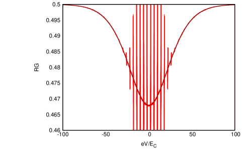
A very useful application of double junction structures with normal-metal electrodes (NININ) is for temperature measurements. Consider such a structure, with charging energy of the island denoted as before by and at temperature (assuming equilibrium) . Clear Coulomb-blockade effects can be seen if the temperature is much smaller than the charging energy: the current is zero for voltages lower then , as it takes that much energy to add an electron on the island. Plateaus are then formed at values of the bias voltage corresponding to multiples of (see Figure 4 left). The conductance curves then show so-called Coulomb-blockade oscillations (see Figure 4) right). Gate voltages can be also included in this analysis, in which case it can be shown that, in the gate voltage – bias voltage space the stable states (corresponding to different numbers of electrons on the island) form a diamond pattern al .
We now examine the effect of temperature: intuitively, as the temperature is increased, one expects that the features visible at low temperatures will be smeared out and eventually washed away. Surprisingly however, if the temperature is larger than the charging energy, one clear feature survives in the conductance, namely a dip at low bias voltages. It can be shown cbt , within the orthodox theory presented above, that, in the limit , the full width of this Coulomb blockade dip (measured half-way between the dip in the conductance at zero bias and the plateau at ) is given by
| (48) |
and the relative change of conductance at zero bias voltage is
| (49) |
It is straigthforward to show that , meaning that at large bias voltage the charging energy of the island does not have any effect and the conductance of the NININ array becomes that of two junctions of resistance in series. Eq. (48) enables the use of such structures as primary thermometers: from a simple measurement of conductance it is possible to extract without any need for calibration. Eq. (49) can be used to determine .
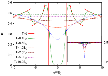
What happens now if the electrodes become superconducting? In Figure 5 left we present the behavior of the Coulomb blockade dip for a SINIS structure as the gap of the electrodes is increased. One can see how the superconducting gap is introducing additional features into the conductance curve which, as the gap is gradually increased, finally distort its shape so much that the CBT dip is very soon not distinguishable anymore. The origin of these features is described in detail in Section III.4.
III.3 SINIS
A superconductor-insulator-normal metal-insulator-superconducting (SINIS) device can be seen as an SET without gate, with superconducting leads and a normal metal island. SINIS are very useful devices, used as local coolers microcoolers , secondary thermometers koppinen_thermometry , and electron pumps pump . Usually the charging energy in a SINIS is so small that it can be neglected. However, in some applications, for instance as thermometers, the SINIS dimensions may become small enough to make charging effects become observable.
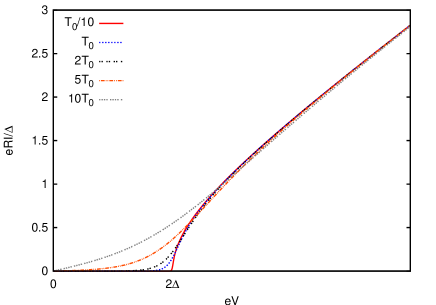
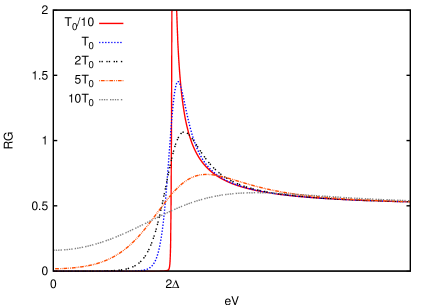
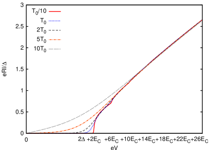
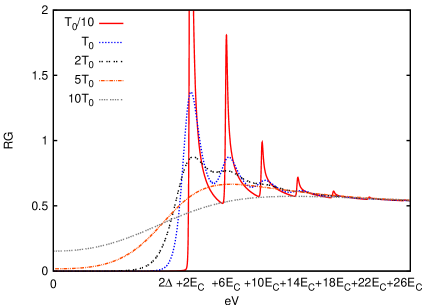
Figure 6 shows the –-curves and conductances of a SINIS structure at different operating temperatures for both zero and finite charging energy. Without charging energy, the SINIS reproduces the – curve of a single NIS junction, with all features being at twice the voltage, as we expect due to the fact that only half of the voltage applied to the SINIS drops over a single junction. With a finite charging energy, the quasiparticle threshold is pushed up from to , and is repeated at intervals with decreasing amplitude. This is visible especially well in the conductance plots in Fig. 6. At operating temperatures that are comparable to or larger than the charging energy, all features are smeared out. In Fig. 6 (for the case that eV and thus eV), the curve with still barely visible oscillations conductance would correspond to a temperature of eV, while in the curve at the next higher temperature of eV the oscillations are smeared out entirely.
III.4 Superconducting SETs
When also the island becomes superconducting, we differentiate between two cases, the symmetric SSET, where the gaps (denoted by ) of both leads and island are identical, and the asymmetric SSET, where the gap in the island differs from the gaps in the leads (denoted by and , respectively). For simplicity of the further discussion, we introduce two new notations, namely the sum of the lead and island gaps,
| (50a) | |||
| and the difference between the gaps, | |||
| (50b) | |||
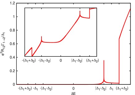
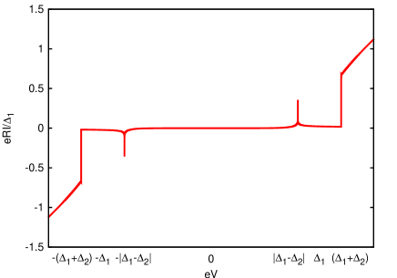
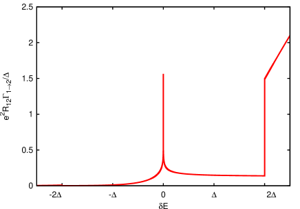
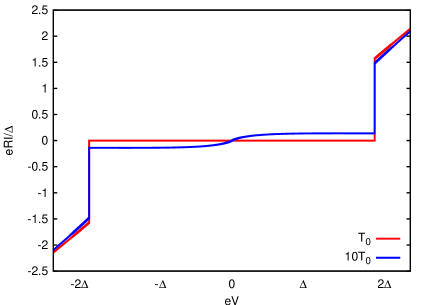
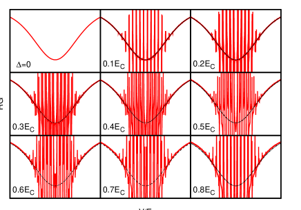
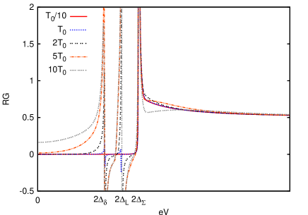
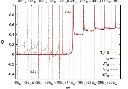
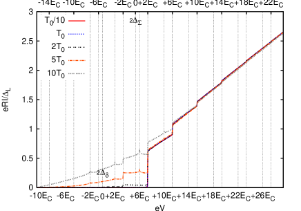
Figure 7 shows the – characteristics of an asymmetric SET with and for different temperatures. Compared to the – of a SINIS structure, we can see the appearance of a new feature, the singularity-matching peak, which apears at voltages . As mentioned above, these peaks appear because of the overlap of two infinite density of states appearing under the integral giving the tunneling rates. Singularity-matching peaks in superconducting single-electron transistors have been investigated theoretically previously in korotkov and first observed experimentally by nakamura and pekola . In NbAlNb structures subgap features at have been observed in klapwijk . Also in this figure we see the usual feature due to quasiparticle threshold at . Finally, a third peak appears at , where the upper and lower singularity in the density of states of the left and right lead, respectively, are aligned. The right plot in Figure 7 shows the conductance for the same values. The conductance plot is perhaps not as descriptive as the one of a SINIS, but it still serves two purposes: 1) it emphasizes very well all sharp features and thus makes it easy to determine their position and, 2) it allows to easily distinguish between singularity matching peak- and quasiparticle threshold-like features, as the latter only produces an upward spike, while the former produces a double spike, with the second spike going downwards. This is especially useful when discussing SSETs with charging energy, where one can find a large amount of weak features.
At finite charging energies, we see a similar repetition of features as one sees in SINIS –s with . These features are a combination of the usual coulomb blockade features in normal metal SETs and a series of peaks and steps. The origin of the peaks are the singularity matching peaks in the tunneling rates (13). Their positions are easily calculated by equating the energy differences of Eq. (36) with the positions of the singularity matching peaks , and solving for the applied voltage.
To get a feeling of how these features enter the –-curve, we first look at the special case of two identical junctions, where . In this setup, we have that . For further simplification, we also set the gate charge equal to zero, i.e. . If we now for instance look at the series of peaks that correspond to , we find , and therefore . Altogether we find that the bias voltages at which peaks occur (at ) are
| (51) |
Similarly, the – shows a series of positive and negative steps. These steps originate from the quasiparticle threshold in the tunneling rates (13). We can find them in a similar manner as the peaks, by equating Eqs. (36) with and find
| (52) |
Equation (52) corresponds to positive steps for , and to negative steps for . The negative steps however, which are already small in the tunneling rates, are difficult to observe in practice.
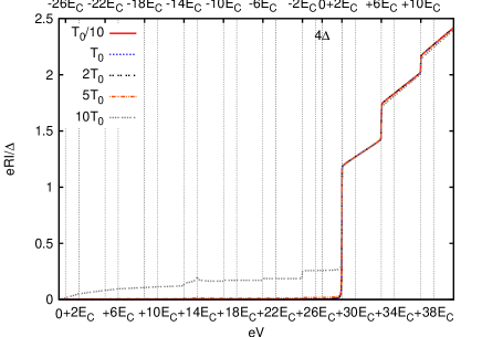
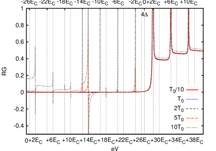
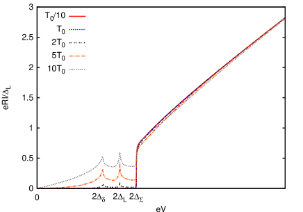
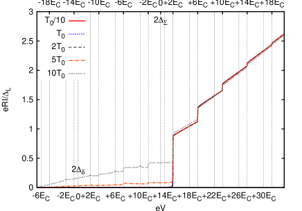
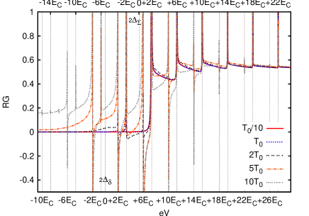
Figures 8, 9 and 10 show the – and conductance of SSETs with a finite charging energy of , with ratios between island and lead gaps of , and , respectively. In all figures one can see the distribution of peaks and steps as described in Eqs. (51) and (52), with growing complexity. In the – curves, especially in Figure 8, the features are difficult to distinguish. Therefore the conductance plots become a powerful tool in identifying the position of peaks and steps, and in distinguishing between them (single and double spikes in conductance correspond to steps and peaks, respectively, in current).
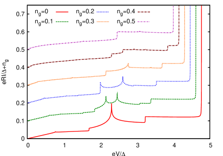
III.5 Effect of the gate
To study how the gate charge affects the IV-curves of an SSET, it is best to do some simplifications again, to somewhat limit the amount of confusing details. In Fig. 11 we have reproduced the first figure of nakamura , where the IV of a symmetric SSET was studied. The figure shows a set of IV curves through the SSET as function of bias voltage for different values of the gate charge. As one can see, also here appears a series of peaks and steps, but their position is shifted as the gate charge is altered. Again the position of the features is easily calculated by equating the energy differences (for the most general case, use (39)) to for peaks, and for steps. As in this case , the equation for the position of the peaks is somewhat simplified, as here the derived voltages will not depend on the superconducting gap. As in nakamura , the positions of the peaks in the system at hand (where possibly ) are given by
| (53) |
Here we defined , with the gate charge and the background charge of the island. Accordingly, the positions of the positive and negative steps are given by
| (54) |
Here the positive steps are obtained for the sign in from of the fraction , and the negative steps are obtained for a sign in front of the same fraction. The negative steps can be observed only at higher temperatures – see the comments on the height of the quasiparticle threshold, Eq. (27) and (27); only the positive steps are visible in Figure (11).
It is easy to verify that Eqs. (51) and (52) are another case of the expressions derived above Eqs. (54-53); these sets of equations become identical when using the same assumptions (identical junctions and =0), and remembering that here and .
III.6 Cooling
Tunneling of electrons through junctions results in energy being transferred between the electrodes, as the higher energetic electrons are extracted or pumped from or into one of the electrodes. In the case of two-junction structures such as SETs, SINIS, etc., this results in the heating and cooling of the middle electrode (the island). This is due to the fact that, although the currents through the two junctions are the same, as it should be due to the conservation of charge (the charge of the island has to remain constant) the energy transfer (heat) does not need to satisfy such a conservation law.
It is straightforward to calculate the energy transferred per unit time out of the island (cooling power) as a function of the applied voltage,
| (55) |
Here the powers , , , and correspond to energy being transferred onto/off the island by tunneling into the left and right electrodes, at a given number of excess electrons on the island. They can be calculated by multiplying the energy carried by each tunneling electron to the probability of tunneling per unit time (given by the density of states and Fermi factors), and then summing over energy states (see also Eqs. (13a), (13b)),
| (56a) | |||||
| (56b) | |||||
where .
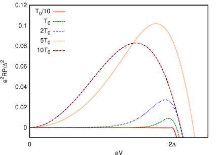
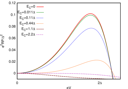
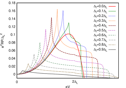
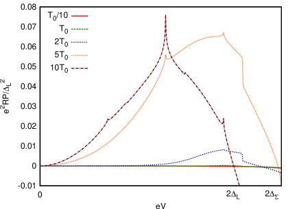
In Figure 12 we present a comparison between the cooling powers on the island Eq.(55) for SINIS (upper plots) and superconducting SET structures (lower plots). We observe that cooling exists only in an interval of bias voltages not much larger than the quasiparticle threshold at (we take identical superconducting leads with gap ). As seen from the left upper plot, as the temperature is lowered the process becomes much less efficient. The general effect of the charging energy is that it is detrimental to cooling (right plot, upper part). In the case of superconducting SET’s (lower plots, Figure 12) the existence of singularity-matching peaks produces relatively sharp spikes in the cooling power. Essentially, the island is cooled down by BCS quasiparticles manninen . The left figure shows these features for the case of negligible charging energy (a SISIS structure with a relatively large middle electrode having a different gap than the leads). An interesting feature is also that the range of voltages over which cooling occurs is extended, due to the fact that now the quasiparticle threshold is at values . Finally, cooling in SET structures with finite charging energy is shown in the lower-right plot of Figure 12.
IV Conclusions
We have presented the theory of tunneling in metallic and superconducting two-junction arrays such as single electron transistors, together with a number of applications. All three energy scales, the charging energy, the superconducting gap, and the temperature, are considered and their role is thoroughly discussed. For example, we examined how a finite superconducting gap affects the Coulomb-blockade based thermometry, the effect of singularity-matching peaks in the current-voltage and conductance-voltage characteristics of superconducting single-electron transistors, and we looked at the effect of charging energy in cooling devices. With the development of the field of nanotechnology, such devices could emerge as very useful tools for high-precision measurements of nano-structured materials and objects at low temperatures.
Appendix A A useful integral
For completeness, we give a full derivation of the result Eq. (6) (see e.g. ingold ). The Fermi functions are given by
| (57) |
We now introduce the function
| (58) |
Obviously . The first derivative of gives
| (59) |
This means that , so we have the result
| (60) |
Now, integrals over expressions of the type , which appear in the theory of tunneling due to Pauli exclusion principle, can be solved by noticing that
| (61) |
where . Now, using Eq. (60) we get immediately
| (62) |
Appendix B Derivation of some integral expansions used
Generic procedure: In the following we want to derive the expansion of Eq. (22). To get a feeling for the procedure, we will first consider a somewhat easier and more common integral, namely
| (63) |
which we assume to not be solvable analytically. For the function we assume that it is well behaved for all and that behaves as for large . However, is logarithmically divergent for . We can separate into a divergent and an non-divergent part by performing a partial integration,
| (64) |
Here the first term is an explicit expression that describes the divergence around and the second term is a finite integral that needs to be computed numerically (we use the notation ). Unfortunately, the function over the integral in the second term of Eq. (64) has no Taylor expansion in , making any further analysis of the integral difficult. It is however possible to find an expansion by doing repeated partial integration. If we define the function such that
| (65) |
it is easy to show that
| (66) |
where is the harmonic number (we could actually still add an arbitrary polynomial of th order to , but due to the repeated partial integrations all its coefficients cancel out and we therefore set them equal zero). These functions have the properties , and . With this we can write as
| (67) |
where by we denote the th derivative of , .
Application: In Section II, we have encountered slightly more complicated integrals, which were of the form
| (68) |
with a logarithmic singularity in . For this reason we would like to expand after the recipe that was used when expanding the previous integral, Eq. (63). The only complication we encounter is that we need to find a function with and
| (69) |
It is easy to verify that the function is given by
| (70) |
The general function can be found with the trial solution
| (71) |
where and are polynomials. By inserting Eq. (71) into Eq. (69), we find that and must fulfill the relations
| (72) |
and
| (73) |
These relations can finally shown to be fulfilled if
| (74a) | |||||
| (74b) | |||||
where
| (75a) | |||||
| (75b) | |||||
Although these polynomials look somewhat complicated, only the constant term in will enter the expansion of ,
| (76) | |||||
where the first term of Eq. (76) contains the convergence for .
The convergence of expression (76) is somewhat tricky to show as it depends on the values of the function and its derivatives at . With the ratio test of convergence for infinite series we find, writing Eq. (76) as , that
| (77) | |||||
which is smaller than one if increases slower than . For example, if , we would have , which tends to zero for large , and thus the series would be convergent.
Acknowledgements.
We would like to thank J. P. Pekola and I. Maasilta for useful comments on the manuscript. T. K. would like to acknowledge financial support from the Emil Aaltonen foundation. The contribution of G.S.P. was supported by the Academy of Finland (Acad. Res. Fellowship 00857, and projects 129896, 118122, and 135135).References
- (1) D. V. Averin and K. K. Likharev, J. Low Temp. Phys. 62, 345 (1986); T. A. Fulton and G. J. Dolan, Phys. Rev. Lett. 59, 109 (1987).
- (2) R. J. Schoelkopf, P. Wahlgren, A. A. Kozhevnikov, P. Delsing, and D. E. Prober, Science 280, 1238 (1998); M. A. Sillanpä,̈ L. Roschier, and P. J. Hakonen, Phys. Rev. Lett. 93, 066805 (2004).
- (3) M. H. Devoret, R. J. Schoelkopf, Nature 406, 1039 (2000).
- (4) Y. Nakamura, Y. A. Pashkin, and J. S. Tsai, Nature, 398, 786 (1999); Yu. Makhlin, G. Schn, and A. Shnirman, Rev. Mod. Phys. 73, 357 (2001); D. Vion et. al., Science 296, 886 (2002); Y. Nakamura, Yu. A. Paskin, T. Yamamoto, and J. S. Tsai, Phys. Rev. Lett. 88, 047901 (2002); Yu. A. Paskin et. al., Nature 421, 823 (2003); T. Yamamoto et. al., Nature 425, 941 (2003); T. Duty, D. Gunnarsson, K. Bladh, and P. Delsing, Phys. Rev. B 69 132504 (2004); J.Q. You and F. Nori, Physics Today 58, 42 (2005); G. S. Paraoanu, Phys. Rev. B 74, 140504(R) (2006). G. S. Paraoanu, Phys. Rev. Lett. 97, 180406 (2006); J. Li, K. Chalapat, and G. S. Paraoanu, Phys. Rev. B 78, 064503 (2008); J. Li and G.S. Paraoanu, New J. Phys. 11, 113020 (2009).
- (5) G. S. Paraoanu and A. M. Halvari, Appl. Phys. Lett. 86, 093101 (2005); T. F. Li et. al., Appl. Phys. Lett. 91, 033107 (2007).
- (6) J. P. Pekola, K. P. Hirvi, J. P. Kauppinen, and M. A. Paalanen, Phys. Rev. Lett. 73, 2903 (1994); K. P. Hirvi, J. P. Kauppinen, A. N. Korotkov, M. A. Paalanen, and J. P. Pekola, Appl. Phys. Lett. 67, 2096 (1995); J. P. Kauppinen and J. P. Pekola, Phys. Rev. Lett. 77, 3889 (1996); Sh. Farhangfar, K. P. Hirvi, J.P. Kauppinen, J. P. Pekola, J. J. Toppari, D. V. Averin, and A. N. Korotkov, J. Low Temp. Phys. 108, 191 (1997); J. P. Pekola, J. J. Toppari, J. P. Kauppinen, K. M. Kinnunen, A. J. Manninen, and A. G. M. Jansen, J. Appl. Phys. 83, 5582 (1998); J. P. Kauppinen, K. T. Loberg, A. J. Manninen, J. P. Pekola, and R. V. Voutilainen, Rev. Sci. Instrum. 69, 4166 (1998).
- (7) M. M. Leivo, J. P. Pekola, and D. V. Averin, Appl. Phys. Lett. 68, 1996 (1996); J. P. Pekola, F. Giazotto, and O.-P. Saira, Phys. Rev. Lett. 98, 037201 (2007); O.-P. Saira, M. Meschke, F. Giazotto, A. M. Savin, M. Mottonen, J. P. Pekola, Phys. Rev. Lett. 99, 027203 (2007).
- (8) A. B. Zorin, S. V. Lotkhov, H. Zangerle, and J. Niemeyer, J. Appl. Phys. 88, 2665 (2000); R. Dolata, H. Scherer, A.B. Zorin, V. A. Krupenin, J. Niemyer, Appl. Phys. Lett. 80 2776 (2002); N. Kim et. al., Physica B 329-333 (2003), 1519; G. S. Paraoanu and A. Halvari, Rev. Adv. Mater. Sci. 5, 265 (2003); M. Watanabe, Y. Nakamura, J.-S. Tsai, Appl. Phys. Lett. 84 410 (2004); A. M. Savin et. al., Appl. Phys. Lett. 91, 063512 (2007).
- (9) J. Bardeen, Phys. Rev. Lett. 6 57 (1961).
- (10) F. Giazotto, T. T. Heikkilä, A. Luukanen, A. M. Savin, and J. Pekola, Rev. Mod. Phys. 78, 217 (2006).
- (11) G.-L. Ingold and Yu.V. Nazarov, ”Charge tunneling rates in ultrasmall junctions”, in Single Charge Tunneling, edited by H. Grabert and M. H. Devoret (Plenum, New York, 1992), pp. 21-108.
- (12) G. Schön, ”Single-electron tunneling”, in T. Dittrich, P. Hänggi, G. Ingold, B. Kramer, G. Schön, and W. Zwerger, Quantum Transport and Dissipation (VCH Verlag 1997), Chapter 3.
- (13) W. A. Harrison, Phys. Rev. 123, 85 (1961).
- (14) J. G. Simons, J. Appl. Phys. 34, 1793 (1963); T. E. Hartman, J. Appl. Phys. 35, 3283 (1964); W.F. Brinkman, R. C. Dynes, and J. M. Rowell, J. Appl. Phys. 41, 1915 (1970);
- (15) W. A. Hofer, A. S. Foster, and A. S. Shluger Rev. Mod. Phys. 75, 1287 (2003).
- (16) P. Törmä and P. Zoller, Phys. Rev. Lett. 85, 487 (2000); Gh.-S. Paraoanu, M. Rodriguez, and P. Törmä, J. Phys. B. 34, 4763 (2001); Gh.-S. Paraoanu, M. Rodriguez, and P. Törmä, Phys. Rev. A 66, 041603 (2002); J. Kinnunen, M. Rodriguez, and P. Törmä, Science 305, 1131 (2004).
- (17) R. C. Dynes et. al., Phys. Rev. Lett. 53, 2437 (1984); M. Kunchur et. al., Phys. Rev. B 36, 4062 (1987); J. P. Pekola et. al., Phys. Rev. Lett. 92, 056804 (2004).
- (18) J. J. Toppari, T. Kühn, A. P. Halvari, J. Kinnunen, M. Leskinen, and G. S. Paraoanu, Phys. Rev. B 76, 172505 (2007).
- (19) J. J. Toppari, T. Kühn, A. M. Halvari, and G. S. Paraoanu, J. Phys.: Conf. Ser. 150, 022088 (2009).
- (20) Y. T. Tan, T. Kamiya, Z. A. K. Durrani, and H. Ahmed, J. Appl. Phys. 94, 633 (2003); K. Luo, D.-H. Chae1 and Z. Yao, Nanotechnology 18 465203 (2007).
- (21) H. van Houten, C.W.J. Beenakker, and A.A.M. Staring, ”Coulomb-blockade oscillations in semiconductor nanostructures”, in Single Charge Tunneling, edited by H. Grabert and M. H. Devoret (Plenum, New York, 1992), pp. 167-216.
- (22) S. Kafanov, A. Kemppinen, Yu. A. Pashkin, M. Meschke, J. S. Tsai, and J. P. Pekola , Phys. Rev. Lett. 103, 120801 (2009).
- (23) D. V. Averin and K.K. Likharev, ”Single electronics: a correlated transfer of single electrons and Cooper pairs in systems of small tunnel junctions”, in B. L. Altshuler, P. A. Lee, and R. A. Webb, Mesoscopic phenomena in solids, Elsevier Science Publishers, 1991.
- (24) P. J. Koppinen, T. Kühn, and I. J. Maasilta, J. Low. Temp. Phys. 154, 179 (2009).
- (25) J. P. Pekola, J. J. Vartiainen, M. Möttönen, O.-P. Saira, M. Meschke, and D. V. Averin, Nature Phys. 4, 120 (2008).
- (26) A. N. Korotkov, Appl. Phys. Lett. 69 2593 (1996).
- (27) Y. Nakamura, A. N. Korotkov, C.D. Chen, and J. S. Tsai, Phys. Reb. B 56, 5116 (1997).
- (28) A. J. Manninen, Yu. A. Pashkin, A. N. Korotkov, and J. P. Pekola, Europhys. Lett. 39, 305 (1997).
- (29) M. G. Blamire, E. C. G. Kirk, J. E. Evetts, and T. M. Klapwijk, Phys. Rev. Lett. 66, 220 (1991).
- (30) A. J. Manninen, J. K. Suoknuuti, M. M. Leivo, and J. P. Pekola, Apl. Phys. Lett. 74 3020 (1999).