Reconfigurable nanoelectronics using graphene based spintronic logic gates
Abstract
This paper presents a novel design concept for spintronic nanoelectronics that emphasizes a seamless integration of spin-based memory and logic circuits. The building blocks are magneto-logic gates [1] based on a hybrid graphene/ferromagnet material system. We use network search engines as a technology demonstration vehicle and present a spin-based circuit design with smaller area, faster speed, and lower energy consumption than the state-of-the-art CMOS counterparts. This design can also be applied in applications such as data compression [2, 3, 4, 5], coding [6] and image recognition [7, 8]. In the proposed scheme, over 100 spin-based logic operations are carried out before any need for a spin-charge conversion. Consequently, supporting CMOS electronics requires little power consumption. The spintronic-CMOS integrated system can be implemented on a single 3-D chip. These nonvolatile logic circuits hold potential for a paradigm shift in computing applications.
Index Terms:
spintronics, network search engines, content addressable memoryI Introduction
The continued Moore’s law scaling in CMOS integrated circuits poses increasing challenges to provide low-energy consumption, sufficient processor speed, bandwidth of interconnects, and memory storage [9, 10]. CMOS logic circuits rely on the von Neumann computer architecture consisting of central processing units (CPU) connected by some communication channel to memory. The bottleneck caused by the communication (sometimes dubbed as the von Neumann bottleneck) and memory accesses is the underlying reason for the significant and widening gap between the fast improving transistor performance and our relatively stagnant ability to provide correspondingly faster program executions. Such bottlenecks are especially obvious for data intensive applications where most of the actions involve accessing or checking data (rather than doing complex computation). Network routers are a classical example where the Internet protocol (IP) address is compared to a list of patterns to find the best match for further processing. In a typical router, special-purpose associative tables are used where the search data (the key) is simultaneously compared with all of the table entries to find matches. Such tables allow us to fundamentally improve the processing speed. Unfortunately, conventional CMOS implementation of these circuits also suffer from scalability issues, making them ineffective for larger search problems that are increasingly relevant to modern workloads.
In this paper, we propose a paradigm change for these search applications using spintronics, which posses fundamental advantages over CMOS in chip area and power consumption. Specifically, we demonstrate a 3.2-Mbit spintronic search engine with 25K words of 128 bits using 0.04-m2 bit cells, designed and simulated using device and circuit simulation. In this design, the total chip area is less than 1 mm2. For the same die size, Analog Bits, Inc. provides a macro 50x smaller (64Kb) using TSMC 0.13 technology. Also for comparison, the reported package size of a state-of-the-art CMOS based search engine is 729 mm2 (Renesas R8A20410BG; 20 Mbits). As important, the total power consumption of this spintronic search engine without any design optimization is smaller than state-of-the-art CMOS based search engines. The proposed spintronic circuit architecture can also enhance a variety of applications that benefit from massive parallel search operations (e.g.; data compression [2, 3, 4, 5], coding [6] and image recognition [7, 8]).
This paper is organized as follow. Section II discusses the MLG basic device operation. It includes explanations on the materials choice and on spin properties. In Sec. III we present the spintronic search engine circuit design and we discuss its efficient searching methods as well as some of its scaling merits. Section IV discusses a proposed spintronics-CMOS interface which is then simulated by an advanced design system. In this part we also discuss power dissipation aspects. In Sec. V we briefly mention other potential applications of the proposed spintronic system and in Sec. VI we summarize our findings.
II The building block: Magneto-Logic Gate (MLG)
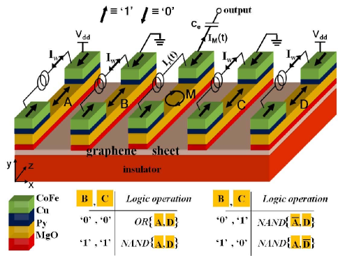
A magneto-logic gate (MLG) is adopted as the basic building block due to its potentially favorable properties of spin amplification, speed and scalability [1]. Fig. 1 shows a universal and reconfigurable MLG that consists of five ferromagnetic (FM) electrodes on top of a graphene layer. FM regions are inherently nonvolatile, they preserve the direction of magnetization even in the absence of any power supply. While this feature has been extensively used for robust information storage in magnetic hard drives and magnetic random access memories (MRAMs) [11], here we show how this nonvolatility can also be used for high-performance magneto-logic. The magnetization itself reflects that the FM electrode has an unequal number of electrons with two different spin projections (up and down; minority and majority). The MLG design employs a stack of FM layers where the elongated permalloy layer (Py) is the free magnetic layer into which the information is encoded. Details of the FM layered system will be explained in Sec. II-A. The MLG operation relies on the generation of non-equilibrium spin accumulation when spin polarized electrons tunnel from the free layer into the graphene via the MgO tunneling barrier. The magnitude of the spin accumulation in the graphene strongly depends on the relative orientation of the magnetization directions in the free layers of the MLG. Of the five FM contacts, the middle contact (M) is used for readout and the remaining four contacts (A, B, C & D) are logic operands whose values are defined by the magnetization direction (‘0’ & ‘1’ in Fig. 1). The output state is given by the Boolean expression (A xor B) + (C xor D). By reprogramming the B and C states we get a universal set of four logic operations between A and D.
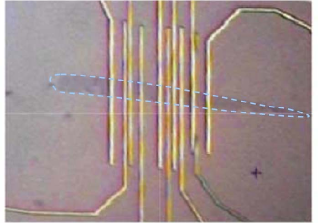
The logic operation is triggered by perturbing the magnetization direction of M. The electrical response to the perturbation is governed by the potential level in the middle contact. In steady-state, the potential level is set by the zero electrical current condition, =0, due to the external capacitor, . In the case of small external and intrinsic device capacitance, the response is instantaneous and the potential level ‘follows’ the magnetization direction. The transient current response depends on the of the system and on the spin-accumulation profile in the graphene layer. This profile is a function of the magnetization alignment of contacts A-D [1]. Examples of the potential level and transient current responses will be discussed in Sec. II-B. In the original MLG design, semiconductors were employed as the spin transport channel. Here, we propose to use graphene due to its robust room temperature spin transport and high mobility [12, 13, 14, 15]. Figure 2 shows an optical microscope image of a lateral graphene sheet topped with ferromagnetic contacts. Note the similarity to the proposed MLG. Non-local spin-valve measurements of this device at room temperature measurements yielded a spin-diffusion length of 3 m in the graphene sheet [15].111In measurements of non-local spin-valve devices, a charge current flows between two biased FM contacts that are spaced by a non-magnetic material (graphene in this case). The generated non-equilibrium spin accumulation in the non-magnetic material is then measured by the change in the potential level of nearby FM contacts outside the region of the charge current flow. The long spin diffusion length at room temperature is a unique property of graphene that could be further improved with material optimization. The use of tunnel barriers has recently improved the spin polarization of injected carriers to 30% [15].
II-A MLG Design: Writing Logic Operands and Readout
Another novelty in the MLG design of Fig. 1 is the spin-transfer torque (STT) magnetization writing [16, 17, 18]. Each of the FM contacts employs an all-metallic path with ultra-low resistance for the writing current () during the operand writing phase of the MLG [19, 20]. This path allows significant energy savings compared to the standard STT pillar technique based on a magnetic tunnel junction [21, 22] in which the writing current flows through the MgO tunneling barriers and graphene. In the writing scheme depicted in Fig. 1, the magnetic moment of the free layer (Py) of a logic operand contact (A-D) is switched by applying a nanosecond-scale current pulse between the two top CoFe layers of the operand contact. The magnetization directions of all CoFe regions are fixed (hard layers). A write current pulse in the opposite direction switches the magnetic moment of the free layer of the operand contact to the opposite orientation.
There are three possible readout schemes for the MLG logic output, all by perturbing the magnetization direction of the free layer in the middle contact, but relying on different configurations of magnetization of the fixed layers of the middle contact. In the first scheme, the fixed layer magnetic moment directions in the middle contact are the same as those of the operand contacts as shown in Fig. 1. For this configuration, the readout is performed during rotation of magnetization of the free layer in response to a read current pulse in the shape of a single period of a sinusoid. Such a read current pulse of sufficient magnitude switches the magnetic moment of the free layer back and forth and thus results in a rotation of magnetization of the free layer in the plane of the sample by 360∘. In the second readout scheme, the magnetic moments of the fixed layers are rotated clockwise by 90∘ in the plane of the sample compared to the directions shown in Fig. 1. For this scheme, a positive read current pulse rotates the free layer moment in the sample plane by 90∘ followed by rotation of magnetization back to the original direction after the read current pulse. The advantage of this scheme is a smaller perturbing read current because perpendicular direction of the fixed layer moment maximizes spin torque magnitude [16]. In the third scheme, the fixed layer moments are perpendicular to the sample plane. In this configuration, the free layer moment rotates by 360∘ in response to a short positive read current pulse [23, 24]. The fixed layer magnetic configurations for the first two readout schemes can be achieved via a combination of exchange bias and magnetic shape anisotropy [25]. The magnetic configuration of the third readout scheme can be achieved via the use of magnetic materials with perpendicular magnetic anisotropy [26]. In the following text, we assume the first readout scheme is used, but the other two schemes can be applied without much difficulty.
II-B Device Simulation
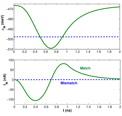
The readout operation of a single MLG is simulated during a 1 ns in-plane full rotation of the magnetization of the middle contact. The electrochemical potential level in the middle contact () and the transient current across it () are shown in Fig. 3. In this example the output node (see Fig. 1) is grounded and the external capacitor is =1 fF. If the search key (encoded in both contacts A & D) match/mismatch the stored bit (encoded in both contacts B & C) then the transient response is significantly larger/smaller. We duplicate the encoding of the search and stored bits in two contacts each in order to account for the possibility of ‘don’t care’ bits (section III). The responses in Fig. 3 are modeled via a diffusive transport model in the graphene layer which includes the effects of traversing under the finite width of the metal contacts and of the intrinsic capacitance across the tunneling barrier. Complete details of the transport model are given in the supplementary material of [1]. We have followed the experimental results of Han et al. [13, 14, 15] and have assumed the following parameters. The contact polarization is 0.3=R↑-R↓/(R↑+R↓) where R↑(↓) is the contact resistance for majority (minority) spins of the ferromagnet, and R=R↑+R↓ is the contact resistance. The sheet resistance in the graphene layer is 1 k, the spin-diffusion length is 3 m, and the diffusion constant is 0.018 m2/s (see Fig. 4(a) in Ref. [15]).
The favorable power scaling with reducing the contact area in STT schemes [27] is an important benefit of MLGs. The area of an MLG can be of the order of 0.01 if the area of each STT contact is 50 nm2 [28]. Below we simulate a 3.2 Mbits spintronic search engine with 25K words of 128 bits using 0.04-m2 MLG cells. In this design, the total circuit area of the MLGs is less than 1 mm2. In comparison, we find two products with the following area specifications. The package size of a state-of-the-art CMOS based search engine is 729 mm2 (Renesas R8A20410BG; 20 Mbits). Another product from Analog Bits, Inc. provides 512x144bits of CAM in a macro of 1mm2 using TSMC 0.13 technology. Furthermore, each cell in a CMOS based search engine consumes about 10 transistors and the cell area can be estimated based on actual designs. Based on the tool provided by Agrawal and Sherwood [29]: such a cell will be 0.55 when implemented with 32 nm CMOS technology. Thus, we expect spintronic designs of search engines to be orders of magnitude smaller. Finally, we note that the area of a reprogrammable and nonvolatile MLG can be further reduced if one uses contacts made of highly anisotropic magnetic materials for which the thermal stability factor is higher [30].
III MLG circuit: spintronic search engine
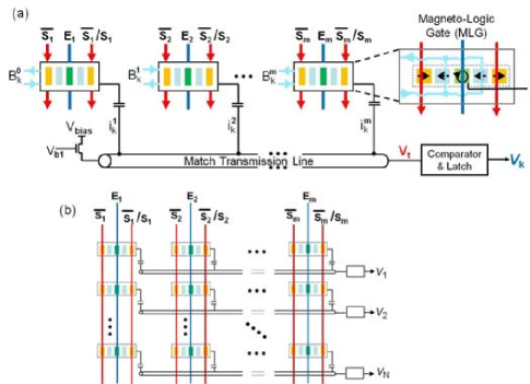
To demonstrate the potential of MLG-based circuits, we use MLGs as building blocks to construct a spintronic search engine, which serves as a technology demonstration vehicle. The associative search of MLGs enables a highly scalable architecture with low power consumption. Fig. 4(a) shows circuitry for one m-bit word in a MLG-based search engine based on STT-MRAM technology. In each MLG, the current direction in one bit-line (vertical red wire) encodes a bit of the input search word at the outer contacts. The inner contacts (not the middle contact) hold the bit of the stored word (written by the horizontal cyan wires). If the stored and search magnetization directions are similar/dissimilar, the spin accumulation in the graphene channel is low/high [31, 32], indicating a match or mismatch. As discussed in Section II, the MLG carries out a XOR operation between the search bit and stored bit, and the matching result can be read by perturbing the middle contact magnetization [1, 33]. When it is not important to match a specific bit (Don’t-Care bit), the left and right outer contacts are magnetized antiparallel (‘0’ and ‘1’), and the MLG always outputs a match.
Fig. 4(b) shows the overall search engine architecture where multiple m-bit rows are stacked to form an Nm bit array, where Nm1. In this configuration, the N MLGs in a column share the same three bit-line currents which either write the search bit (two red vertical lines across the outer contacts) or perturb the middle contact (blue vertical line across the middle contact). Therefore, the current direction in each of these lines can be controlled by a single switch circuit. In conventional STT-MRAM designs, on the other hand, writing to each memory cell requires a dedicated switch circuit to steer the writing current, which can be as large as over 0.1 mA. To reduce the power dissipation of the transistors in the switch circuit, most STT-MRAM designs employ magnetic tunnel junctions since the writing operation in these devices requires smaller current densities than an all-metallic STT cell. As a result, the total power consumption of the transistors and magnetic tunnel junction is reduced in comparison to that with an all-metallic STT cell. Nonetheless, the power-delay product of STT-MRAMs is still poor in comparison with conventional SRAMs (in spite of the improved scaling benefits of STT-MRAMs). The spin-based search engine design alleviates the power-delay problem of STT-MRAMs since N1 writing operations (e.g., in our design example N=25,000) are associated with a steering operation of a single switch circuit. Correspondingly, the MLGs employ all-metallic paths for the currents during the operand writing phase (contacts A-D) and the readout phase (contact M). These ultra-low-resistance paths allow the writing and readout currents to be shared on the same bit line and hence lead to significant energy savings compared to the single-cell read/write operation in standard STT-MRAMs.
Similarly, the proposed spintronic search engine can achieve a substantial improvement in power consumption compared to its CMOS counterparts. In a conventional CMOS search engine, the search bit is distributed as charges to all cells on a bit-line, which is loaded with distributed intrinsic and parasitic capacitance of many thousands of CMOS memory cells. Hence the fan-out limitation of CMOS gates limits the number of words. In our spintronic search engine, the energy consumption of the shared magnetization writing current is potentially much smaller than what is needed to simultaneously charge the bit-line in a CMOS implementation. For example, all of the writing operations in a search engine with 25K words of 128 bits consume 0.15 W, given that the length of each bit line is 1 mm, the cross section is 50 nm by 50 nm, the average metal conductivity is 105 cm-1, and the current is 0.1 mA. As will be shown, this power dissipation is a small fraction of the circuit total power.
One of the key challenges to spintronics lies at the interface between the spin-based devices and supporting CMOS circuitry. Specifically, without consuming significant power, we wish to detect the nA output current pulses from MLGs, and convert them to rail-to-rail digital signals ( in Fig. 4) for CMOS electronics. An MLG generates an output current pulse with a small peak amplitude (100 nA when matched) and duration (1 ns), i.e., a charge of 100 electrons. Hence MLGs operate more like small area DRAM cells but at the speed of larger SRAM cells. The speed and power consumption of MLG-based search engines, therefore, will be largely determined by the sensing scheme. In a conventional CMOS search engine, this task of match-line sensing is typically done by connecting the cells within a word either in a logic wire-OR fashion, or as series transmission gates. For MLG-based search engines, a direct logic wire-OR or transmission-gate structure is difficult to implement because of the analog nature of the MLG output, which is a small current pulse. Further, the detection circuit needs high resolution to resolve the very small difference between a match case and an all-but-one-bit mismatch case.
To achieve the required sensitivity and resolution, we propose a low-noise sensing circuit as shown in Fig. 5. The outputs of all MLGs are connected to a match-line in parallel, and the summed current pulses generate a voltage signal at the input of the detection circuit, which in turn is compared to a reference voltage to generate a digital output, indicating a match or mismatch. Low-noise analog sensing significantly improves the sensitivity compared to a conventional digital sense amplifier. The power consumption of the search engine is kept low by optimizing circuit design and operating it at low duty cycle.
IV A Spintronic Search Engine Design Example
To evaluate the performance of an MLG-based search engine circuit, we design and simulate the prototype circuit in Fig. 5. A circuit model is constructed for a 0.04 m2 MLG device described in Sec. II. The MLG output port is modeled as a pulse current source, and a parasitic resistance and capacitance of the M contact. It also includes a distributed resistance from the M contact to the ground (via the graphene layer and the grounded contacts, B & C), shown as . A coupling capacitor is used to isolate the M contact from the CMOS circuitry in dc, and its value is selected as a trade-off between signal attenuation and the chip area required to implement it on-chip. When the output is short-circuit to ground through , this model can reproduce the MLG transient response in Fig. 3.
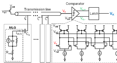
The output current pulses of all cells are summed on the transmission line. Note that this is different from the direct logic wire-OR structure in CMOS search engines in that each MLG behaves like a current source instead of a switch, and exhibits a large impedance to the transmission line in either match or mismatch cases. The high impedance also helps to reduce the crosstalk between the MLGs.222We have also studied an alternative design in which the MLG output is first amplified by a single-transistor amplifier to ensure a good signal-to-noise ratio before pulse combining on the transmission line and to suppress crosstalk. The power consumption of this alternative sensing circuit is more than doubled while the (already negligible) crosstalk between MLGs is further suppressed. The summed current pulses on the transmission line generate a voltage signal at the end of the transmission line ( in Fig. 5). This voltage signal goes to an -stage comparator (=4 in this design example). Then a latch converts the comparator output to a full-swing digital signal, indicating a match or mismatch. The comparator is optimized for small offset voltage and large common-mode-rejection-ratio, which reduce the comparison error. This low-noise analog sensing circuit exhibits good sensitivity and fine resolution with power consumption comparable to a conventional sense amplifier in SRAMs.
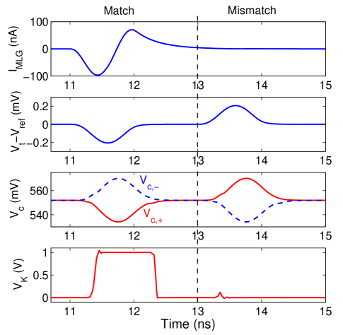
The prototype circuit is simulated using a high speed circuit simulator, Advanced Design System (ADS). The CMOS transistors are based on 45-nm Predictive Technology Model [34], and the power supply voltage is =1 V. Fig. 6 shows the output signal waveforms when the sensing circuit operates at 500 MHz with approximately 50% duty cycle. Fig. 6(a) shows the current signal at the output of the MLG which replicates the match and mismatch signal behaviors in Fig. 3. Fig. 6(b) shows the value of at the input for the sensing circuit. is the transmission line voltage output and simulates the worst case scenario in which 127 out of 128 bits are matched and the current signal of one bit is halfway between a match and a mismatch. Note the opposite polarity of the signal between a match and a mismatch cases. Fig. 6(c) shows the output of the 4-stage comparator, . In all mismatch scenarios, the comparator output is always positive (). The positive amplitude increases with the number of mismatched bits. Only with a line match is negative and is of the order of -20 mV. Fig. 6(d) shows the digital output of the latch.
It is evident that the overall gain is evenly distributed among the stages to achieve the best signal-to-noise ratio and maintain the large bandwidth. The 128-bit match-line sensing circuit can operate up to 500 MHz, and detect MLG output current difference down to 9 nA. The 4-stage comparator and the latch use 0.26 mW. For a 3.2-Mbit search engine (25K words of 128 bits), the total power consumption of these CMOS circuitry is 6.5 W. The power dissipation of each MLG is mostly due to the DC current that flow between the A and B contacts as well as the C and D contacts. In our simulated 200 K contacts and Vdd=1 V applied bias, this corresponds to 5 W per MLG (16 W for 3.2 Mbit search engine). Together with the (much smaller) power consumption of all latches in the sensing circuits and the STT-writing operations, the total power consumption of the MLG-based search engine is about 23 W. In spite of the fact that we have not employed optimization techniques (e.g., pipelined search) this power is already lower compared to optimized CMOS counterpart designs. In addition, using tunneling barriers in the MLG that are more resistive and more spin polarized will keep the MLG current output at the same magnitude but will use less power. For example, if smaller MLG contacts with resistance of R=R↑+R↓=2000 k and polarization of 0.9=R↑-R↓/R can be fabricated then the transient responses are kept similar to those in Fig. 3 but the MLG power dissipation drops by an order of magnitude (from 5 W to 0.5 W per MLG and from 23 W to 9 W for the entire spintronic-CMOS circuit).
The match-line power consumption depends on the MLG output signal amplitude. The larger the output signal, the less gain needed for amplification, and hence less power consumption. In our simulations we have assumed 200:1 MLG output current ratio for match vs. mismatch. The power consumption remains comparable for 10:1 simulated ratio with slight modification of the circuit parameters. It is expected that as the MLG performance improves (larger output signal amplitude, smaller parasitic capacitance and less device variation), the energy efficiency will increase even more since larger number of bits can share the match-line. Correspondingly, the CMOS sensing circuitry needs to improve its resolution.
The circuit area of the sensing circuit is fairly small, and the area overhead is negligible since it is mortgaged by the large number of bits per search word. For example, the aforementioned comparator and latch use a chip area of less than 3 m2 per match-line. In comparison, the conventional CMOS search engine needs a substantial area overhead due to the much shorter search word. Another important issue for a spin-based search engine is the MLG parameter variations. These variations are often being overlooked and their consideration is paramount to any integrated circuit. Without corresponding circuit provisions, the output current variation would fundamentally limit the length of search words (e.g., the fidelity of 128 bits word is the same as of a 128, 87, and 9 bit strings if the MLG output variations are, respectively, 0.1%, 1% and 10%). One way to alleviate the variation concern and yet to achieve longer words is by adopting an offset cancelation technique, i.e., to first calibrate each match-line, and then remove the mismatch between them during the evaluation.
V Potential Applications
In addition to non-volatility, the MLG circuit enables a range of associative computing applications, whereby a large amount of information can be accessed and filtered in parallel with energy efficiency and high speed. As mentioned above, efficient search capabilities are clearly useful in classical examples such as network routing tables. But more importantly, these capabilities can critically impact more complex applications that are limited by the serial communication and processing bottleneck sometimes referred to as the von Neumann bottleneck. Leading examples of applications include the increasingly widely used business analytics and automatic fraud detection that pore over huge amount of data searching for insights. Because of the growing importance of such applications, conventional optimizations are being vigorously pursued in the research community and in commercial products. However, these approaches can reduce some bandwidth wastes but still fundamentally require complete scanning that subjects the large data arrays through the von Neumann bottleneck. In contrast, the underlying MLG circuit allows us to support such applications with a new processing substrate that allows in-memory, massively parallel processing of data and thus enable orders-of-magnitude improvement in processing speed. As an example, conventional business analytics systems are bottlenecked by the sequential scanning of large amount of data that cannot fit on-chip caches. The scanning operations are almost universal simple such as a string and integer comparison. Invariably, such searches return exceedingly small portions of the data (e.g., 0.1%) as results for further processing. MLG search circuit embedded with the storage element thus allows irrelevant data to be filtered out in parallel with essentially constant time and reduce the communication need by orders of magnitude and thus completely eliminate the von Neumann bottleneck.
The logic operations as performed by MLGs also represent a potentially large technology leap for space vehicle processing. Most importantly, it is because the logic operations appear to be inherently radiation hardened. For example, due to the manner in which the logic is stored and read, single event effects should no longer cause upset operations or failures, as could occur in a current field effect transistor. Additionally, the non-volatile logic operations are preserved in the event that systems need to be powered down to protect the electronics. This aspect results in faster times for bringing such systems back online. Finally, the scalability of this circuitry coupled with the reduced power consumption (as compared to current CMOS technology) appears to fit the tight constraints associated with space vehicle electronics designs, opening the door to potential on-board processing.
VI Conclusion
The performance of highly-scalable MLGs will offer much faster operation speed, smaller area, and better energy efficiency than their CMOS counterparts. It is expected that in 5-10 years, the MLG operation speed can reach 0.1 ns, while consuming 0.01 m2 chip area and 100 aJ/operation. It is also envisioned that graphene can be utilized to replace silicon and achieve even greater performance at room temperature. The application of spin-based devices [1, 11] in nonvolatile logic circuits will represent a disruptive advance in the design and implementation of some of the most critical building blocks in general-purpose microprocessors and other high-performance computing and communication systems. It will lead to significant performance gains and energy savings in such systems. Fundamentally, it will enable a paradigm change in computer architectures from von Neumann to one in which memory and processing are seamlessly integrated together.
Acknowledgement
We deeply thank Jiangyun Hu and Jie Zhang for their help in the circuit design and simulations and Ovunc Kocabas for his help in analyzing conventional CAM designs.
References
- [1] H. Dery, P. Dalal, L. Cywinski, and L. J. Sham, “Spin-Based Logic in Semiconductors for Reconfigurable Large-Scale Circuits”, Nature, vol. 447, no. 7144, pp. 573-576, May 2007.
- [2] E. Komoto, T. Homma, and T. Nakamura, “A high-speed and compactsize JPEG Huffman decoder using CAM”, in Symp. VLSI Circuits Dig. Tech. Papers, 1993, pp. 37-38.
- [3] B. W. Wei, R. Tarver, J.-S. Kim, and K. Ng, “A single chip Lempel-Ziv data compressor”, in Proc. IEEE Int. Symp. Circuits Syst. (ISCAS), 1993, pp. 1953-1955.
- [4] R.-Y. Yang and C.-Y. Lee, “High-throughput data compressor designs using content addressable memory”, in Proc. IEEE Int. Symp. Circuits Syst. (ISCAS), 1994, pp. 147-150.
- [5] D. J. Craft, “A fast hardware data compression algorithm and some algorithmic extensions”, IBM J. Res. Devel., vol. 42, no. 6, pp. 733-746, Nov. 1998.
- [6] L.-Y. Liu, J.-F.Wang, R.-J.Wang, and J.-Y. Lee, “CAM-based VLSI architectures for dynamic Huffman coding”, IEEE Trans. Consumer Electron., vol. 40, no. 3, pp. 282-289, Aug. 1994.
- [7] M. Meribout, T. Ogura, and M. Nakanishi, “On using the CAM concept for parametric curve extraction”, IEEE Trans. Image Process., vol. 9, no. 12, pp. 2126-2130, Aug. 2002.
- [8] M. Nakanishi and T. Ogura, “Real-time CAM-based Hough transform and its performance evaluation”, Machine Vision Appl., vol. 12, no. 2, pp. 59-68, Aug. 2000.
- [9] ITRS 2009. [Online]. Available: http://www.itrs.net/links/2009ITRS/Home2009.htm
- [10] S. Rakheja and A. Naeemi, “Interconnects for Novel State Variables: Performance Modeling and Device and Circuit Implications”, IEEE Trans. Electron Devices, vol. 57, no. 10, pp. 2711-2718 , Oct. 2010.
- [11] I. Žutić, J. Fabian, and S. Das Sarma, “Spintronics: Fundamentals and applications”, Rev. Mod. Phys., vol. 76, no. 2, pp. 323-410, Apr. 2004.
- [12] N. Tombros, C. Jozsa, M. Popinciuc, H. T. Jonkman, and B. J. van Wees, “Electronic spin transport and spin precession in single graphene layers at room temperature”, Nature 448, no. 7153, pp. 571-574, Aug. 2007.
- [13] W. Han, K. Pi, W. Bao, K. M. McCreary, Y. Li, W. H. Wang, C. N. Lau, and R. K. Kawakami, “Electrical detection of spin precession in single layer graphene spin valves with transparent contacts”, Appl. Phys. Lett., vol. 94, no. 22, p. 222109, Jun. 2009.
- [14] W. Han, W. H. Wang, K. Pi, K. M. McCreary, W. Bao, Y. Li, F. Miao, C. N. Lau, and R. K. Kawakami, “Electron-hole asymmetry of spin injection and transport in single-layer graphene”, Phys. Rev. Lett., vol. 102, no. 13, p. 137205, Apr. 2009.
- [15] W. Han, K. Pi, K. M. McCreary, Y. Li, Jared J. I. Wong, A. G. Swartz, and R. K. Kawakami, “Tunneling Spin Injection into Single Layer Graphene”, Phys. Rev. Lett., vol. 105, no. 16, p. 167202, Oct. 2010.
- [16] J. C. Slonczewski, “Current-driven excitation of magnetic multilayers”, J. Magn. Magn. Mater., vol. 159, no. 1-2, pp. L1-L7, Jun. 1996.
- [17] L. Berger, “Emission of spin waves by a magnetic multilayer traversed by a current”, Phys. Rev. B, vol. 54, no. 13 , pp. 9353-9358, Oct. 1996.
- [18] J. A. Katine, F. J. Albert, R. A. Buhrman, E. B. Myers, and D. C. Ralph, “Current-driven magnetization reversal and spin-wave excitations in Co/Cu/Co pillars”, Phys. Rev. Lett., vol. 84, no. 14, pp. 3149-3152, Apr. 2000.
- [19] P. M. Braganca, J. A. Katine, N. C. Emley, D. Mauri, J. R. Childress, P. M. Rice, E. Delenia, D. C. Ralph, R. A. Buhrman, “A Three-Terminal Approach to Developing Spin-Torque Written Magnetic Random Access Memory Cells”, IEEE Trans. Nanotech., vol. 8, no. 2, pp. 190-195, Mar. 2009.
- [20] J. Z. Sun, M. C. Gaidis, E. J. O’Sullivan, E. A. Joseph, G. Hu, D. W. Abraham, J. J. Nowak, P. L. Trouilloud, Yu Lu, S. L. Brown, D. C. Worledge, and W. J. Gallagher, “A three-terminal spin-torque-driven magnetic switch”, Appl. Phys. Lett., vol. 95, no. 8, p. 083506, Jul. 2009.
- [21] Y. Huai, F. Albert, P. Nguyen, M. Pakala, and T. Valet, “Observation of spin-transfer switching in deep submicron-sized and low-resistance magnetic tunnel junctions”, Appl. Phys. Lett., vol. 84, no. 16, pp. 3118-3120, Feb. 2004.
- [22] G. D. Fuchs, N. C. Emley, I. N. Krivorotov, P. M. Braganca, E. M. Ryan, S. I. Kiselev, J. C. Sankey, D. C. Ralph, R. A. Buhrman, and J. A. Katine, “Spin-Transfer Effects in Nanoscale Magnetic Tunnel Junctions”, Appl. Phys. Lett., vol. 85, no. 7, pp. 1205-1207, Jun. 2004.
- [23] A. D. Kent, B. Ozyilmaz, E. del Barco, “Spin-transfer-induced precessional magnetization reversal”, Appl. Phys. Lett., vol. 84, no. 19, pp. 3897-3899, May 2004.
- [24] D. E. Nikonov, G. I. Bourianoff, G. Rowlands, I. N. Krivorotov, “Strategies and tolerances of spin transfer torque switching”, J. Appl. Phys., vol. 107, no. 11, p. 113910, Jun. 2010.
- [25] S. O. Valenzuela, M. Tinkham, “Direct electronic measurement of the spin Hall effect”, Nature, vol. 442, no. 7099, pp. 176-179, Jul. 2006.
- [26] H. Meng, J. P. Wang, “Spin transfer in nanomagnetic devices with perpendicular anisotropy”, Appl. Phys. Lett., vol. 88, no. 17, p. 172506, Apr. 2006.
- [27] D. C. Ralph and M. D. Stiles, “Spin Transfer Torques”, J. Magn. Magn. Mater., vol. 320, no. 7, pp. 1190-1216, Apr. 2008.
- [28] H. Yoda et al., “High efficient spin transfer torque writing on perpendicular magnetic tunnel junctions for high density MRAMs”, Curr. Appl. Phys., vol. 10, no. 1, supplement 1, pp. e87-e89, Jan. 2010.
- [29] B. Agrawal and T. Sherwood, “Ternary CAM Power and Delay Model: Extensions and Uses”, IEEE Transactions on VLSI Systems, vol. 16, no.5, pp. 554-564, May 2008.
- [30] S. Ikeda, J. Hayakawa, Y. M. Lee, F. Matsukura, Y. Ohno, T. Hanyu, and H. Ohno, “Magnetic Tunnel Junctions for Spintronic Memories and Beyond”, IEEE Trans. Electron Devices, vol. 54, no. 5, pp. 991-1002 , Nov. 2007.
- [31] H. Dery, L. Cywinski, and L. J. Sham, “Lateral Diffusive Spin Transport in Layered Structures”, Phys. Rev. B., vol. 73, no. 4, p. 041306(R), Jan. 2006.
- [32] H. Dery, L. Cywinski, and L. J. Sham, “Spin Transference and Magnetoresistance Amplification in a Transistor”, Phys. Rev. B., vol. 73, no. 16, p. 161307(R), Apr. 2006.
- [33] L. Cywinski, H. Dery, and L. J. Sham, “Electric Readout of Magnetization Dynamics in a Ferromagnet-Semiconductor System”, Appl. Phys. Lett., vol. 89, no. 4, p. 042105, Jul. 2006.
- [34] W. Zhao and Y. Cao, “New Generation of Predictive Technology Model for Sub-45 nm Early Design Exploration”, IEEE Trans. Electron Devices, vol. 53, no. 11, pp. 2816-2823 , Nov. 2006.