Design and Performance of a Digital Phase Lock Loop for Gunn Oscillators
Abstract
The digital phase lock loop described in this paper has been in use on the Submillimeter Array (SMA) front-end receivers for over a decade and has been a key element in obtaining all of the high quality images that have been published from this telescope over the years. The technical achievements enabled by these devices include the first phase closure observations in the 690 GHz band, the first attempts at band-to-band phase transfer at submillimeter wavelengths, and the first successful demonstration of interferometry using a fully photonic millimeter-wave local oscillator. Copies of these devices are also in place at the Caltech Submillimeter Observatory and the James Clerk Maxwell Telescope in support of the eSMA project and submillimeter VLBI experiments. Additional units of this design were used by the Princeton Millimeter Interferometer and the Microwave Anisotropy Telescope. In total, over three dozen units have been constructed and used in astronomical studies. In this paper, we briefly describe the background theory, design, performance, and calibration steps, and provide useful testing and repair information.
1 Introduction
Operating as a multi-element interferometer, the Submillimeter Array (SMA) located on Mauna Kea, Hawaii enables astronomical imaging with substantially finer angular resolution than the beams achievable by typical single-dish submillimeter cameras and receivers (see e.g. Hunter et al., 1996; Kawamura et al., 1999). Standard radio interferometers require a phase-locked local oscillator (LO) signal in order to achieve frequency conversion from the desired high frequency observing band to a more digitally-accessible intermediate frequency (IF) band (Thompson et al., 2001). The digital phase lock loop (PLL) described in this paper has been in use on the SMA front-end receivers (Blundell, 2005) for over a decade and has been a key element in obtaining all of the high quality, sub-arcsecond images that have been published from this telescope over the years (see e.g. Hunter et al., 2008). The technical achievements enabled by these devices include the first phase closure observations in the 690 GHz band (Hunter et al., 2007), the first phase transfer at submillimeter frequencies (Hunter et al., 2006), and the first successful demonstration of interferometry using a fully photonic millimeter-wave local oscillator (Kimberk et al., 2006). For the latter experiment, a small modification was made to drive a YIG oscillator rather than the standard Gunn oscillator described in the following section.
Copies of the PLL devices and their control software are also in place at the Caltech Submillimeter Observatory (CSO) and the James Clerk Maxwell Telescope (JCMT) in support of the eSMA project, described by Bottinelli et al. (2008). As such, they are also used in current and future submillimeter VLBI observations (Doeleman et al., 2008; Weintroub, 2008). Additional units of this design were used by the Princeton Millimeter Interferometer (MINT) (Doriese, 2002; Fowler et al., 2005) and the Microwave Anisotropy Telescope collaboration of Princeton and University of Pennsylvania (Torbet et al., 1999) both located in the Atacama Desert of northern Chile. In total, over three dozen units have been constructed and used in astronomical studies. In this paper, we briefly describe the background theory, design, performance, and calibration steps, and provide useful testing and repair information. Most of the content of this paper can also be found in SMA technical memo 143111http://www.cfa.harvard.edu/sma/memos/143.pdf.
2 Background: Gunn oscillator frequency tuning
The output frequency of a cavity-tuned Gunn oscillator depends simultaneously on both the electrical and mechanical tuning. Specifically, is a function of the bias voltage and the cavity length :
| (1) |
At a specified tuning point , the function can be approximated by a linear dependence in each variable independently, leading to the following differential equation:
| (2) |
Typically, is listed in units of MHz volt-1 and is positive-valued, while can be interpolated from a micrometer tuning curve listed in units of mil GHz-1 and is negative-valued. With the application of a phase lock loop, can be held constant in time at as it can actively shift the bias voltage by in order to offset temporal changes in the cavity length . Much of is due to drifts in the room temperature. Thus, a successful PLL must be able to maintain lock through a sufficient range of tuning voltage to counteract ambient temperature fluctuations.
3 Design of a Digital PLL
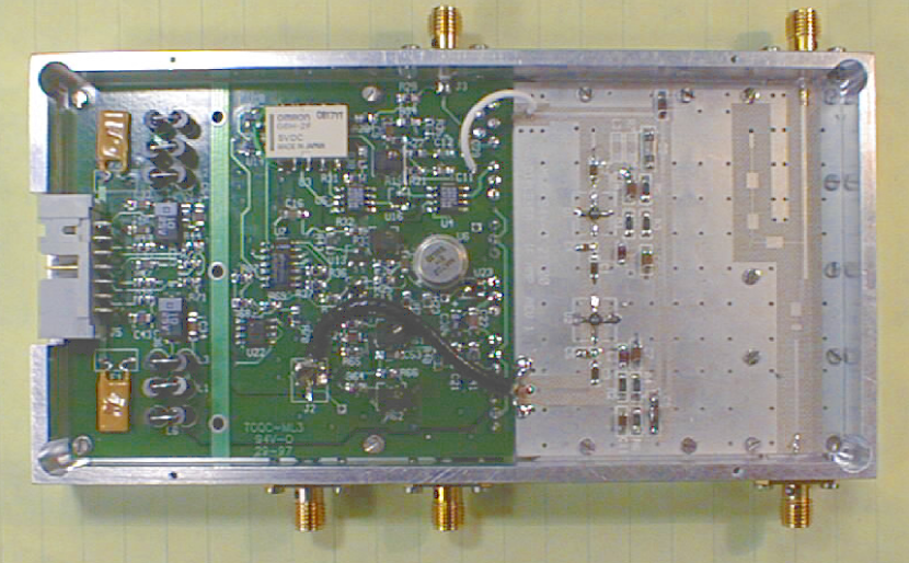
To promote the benefits of modularity and reduce the number of cables emerging from the SMA receiver system optics cage, we decided to provide a PLL for each LO assembly. This requirement set constraints on the size of the unit. Three separate sections comprise the PLL package shown in Figure 1. The righthand side of the PLL box contains a microwave diplexer which allows the high-frequency signal (6-8 GHz) to pass from the YIG reference input out to the harmonic mixer on the LO chain. At the same time, it allows the low frequency mixing product (0-1 GHz) to return from the harmonic mixer and to enter the two-stage IF amplifier.
Gunn bias output Harmonic mixer
IF monitor 109 MHz reference 6-8 GHz reference
control lines
3.1 Diplexer and IF Amplifier
The diplexer substrate is manufactured from Arlon AR1000 Ceramic powder-filled, woven fiberglass, PTFE composite with a dielectric constant of 10. The IF amplifier is comprised of two stages of amplification via Hewlett-Packard INA-02184 Low Noise, Cascadable Silicon Bipolar MMIC Amplifiers for a total gain of dB. This large gain is necessary to process the tiny signal returning from the harmonic mixer (which itself views the Gunn signal through a 20 dB tap). With such a large gain, suppression of noise at the amplifier input port is crucial to prevent oscillation. The tight-fitting lid provides a good mechanical enclosure that prevents any noise coupling. Also, to minimize temperature changes in the unit at power-up time (and the accompanying phase drifts), a heater resistor is installed in the aluminum block which can be enabled by the microcontroller when the PLL/LO chain is turned off.
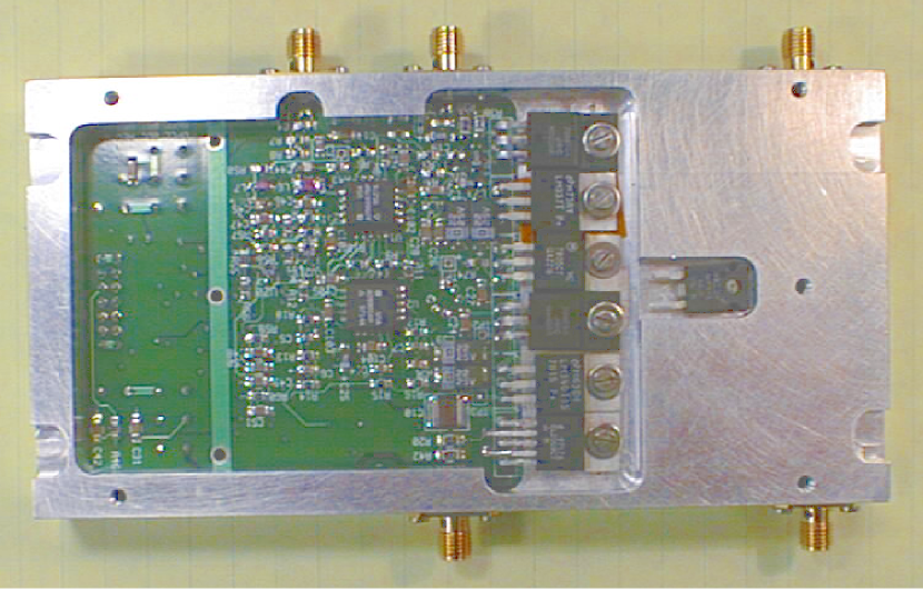
3.2 Phase lock electronics
A good description of PLLs is given by Gardner (1979). Our PLL is based on a high-gain second-order loop with an active filter and a microcontroller interface. A schematic drawing of the circuit can be obtained from the authors upon request. After amplification, the IF signal is passed to the Analog Devices AD96687 Ultrafast ECL Dual Comparator which converts the sinewave to a squarewave. We use zero crossing detection in the comparator in order to avoid the need for an automatic gain control (AGC) circuit in the IF amplifier. Also, by biasing the comparator above the peak value of the IF signal, the microcontroller can effectively disable the loop. The digitized signal output from the comparator enters the Analog Devices AD9901 Ultrahigh Speed Phase/Frequency Discriminator. Here we implement a loop gain control by controlling the current in the AD9901. Specifically, the loop gain of this system (along with the loop bandwidth) is determined by a damping resistor (the parallel combination of potentiometer R19 and resistor R75) and an integrating capacitor (C9). The choice of these values depends on the noise characteristics of the oscillator and the loop performance specifications. For the SMA, the design specification requires the PLL to reacquire lock within s of a Walsh function phase change. The relationships between the rise time () and the 1% settling time of a servo loop () and its undamped natural frequency () are given by:
| (3) | ||||
| (4) |
where is the damping factor and is the negative real part of the pole (Franklin, Powell & Emami-Naeini, 1994). With a reasonable choice of damping factor , we require MHz), which corresponds to:
| (5) |
where is the gain of the tunable oscillator in radian second-1 Volt-1, and is the gain of the phase detector in Volt radian-1. For Carlstrom Gunns (Carlstrom et al., 1985), is on the order of 300 MHz V-1 = 2.0E+09 rad s-1 V-1. For our phase detector (AD9901), the maximum value of is 0.285 Volt radian-1. However, for tuning flexibility, we need to operate at a gain in the middle of this range, so we choose 0.15 V rad-1. With this information in hand, we compute the product (C) must be 2.0E05. In the circuit, we use = 1k to convert the square wave into a DC voltage. This means that C must be 20 nF. Finally, we can relate all of these variables back to the damping factor:
| (6) |
With this condition, we can solve for the final variable, :
| (7) |
An AD817 High Speed, Low Power Wide Supply Range Amplifier provides the loop integrator. A second AD817 monitors the Gunn bias voltage and, along with the Fairchild BAV99LT1 ultrafast diode pair, keeps it within V (i.e. a diode potential) of the target bias voltage set manually via potentiometer R33. The locking sideband can be selected digitally via an Omron G6H-2F DC5 Low Signal Relay. An IF monitor port of dB is provided for viewing the phase lock quality on a spectrum analyzer.
3.3 Lock detection
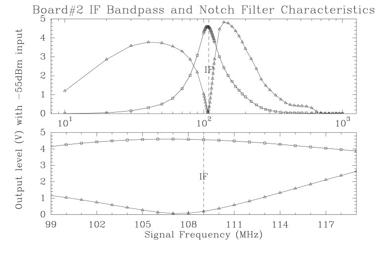
By the nature of the design, phase lock is indicated whenever the gunn bias voltage lies between the two voltage limits established by the diode pair. However, if the IF amplifier is being overdriven, it is possible to acquire “lock” on a harmonic of the IF. To reject these false “locks”, two LC circuits are included which provide a simple yet powerful analysis of the IF to the tuning software. A portion of the IF signal is tapped and sent through a notch filter tuned to 109 MHz and on to an Agilent HSMS2812 Schottky Diode pair. A similar circuit implements a bandpass filter tuned to the same frequency. The voltage outputs of both filter circuits are digitized by the microcontroller board and used in the automated phase lock search algorithm which adjusts the tuning backshort on the Gunn oscillator via a linear actuator while watching these voltages.
IF monitor 109 MHz reference 6-8 GHz reference
Gunn bias output Harmonic mixer
3.4 Control interface
The PLL is controlled through the insulation displacement connector (IDC) port. For manual operation, this port can be connected to a control box with appropriate switches and an external power supply. The remote operation of the PLLs (and their associated LO chains) is achieved via an Intel microcontroller board connected via RS485 to the real-time LynxOS control computer installed in a VME chassis in each antenna. In the laboratory setting, a standard Linux PC can be used instead, along with an RS232/485 converter. In either case, the software program called “tune6” provides a command-line prompt and an RPC server to implement all of the required functionality. For further details, see Hunter et al. (2002).
4 Performance
4.1 Adjacent channel power
The quality of phase lock can be assessed by the amount of power outside of a delta function at the IF frequency compared to the power within the delta function. We refer to this ratio as the adjacent channel power and obtain values of to dBc on Carlstrom Gunns using Pacific Millimeter222http://pacificmillimeter.com/ FMA harmonic mixers (even harmonics only). A representative plot from a spectrum analyzer is shown in Figure 3.

4.2 Walsh functions
Walsh functions are used by radio interferometers to reject noise that can arise in the system between the first LO and the final LO (Thompson et al., 2001). Our PLL easily maintains phase lock throughout the application of phase-switching Walsh functions imposed on the low-frequency 109 MHz reference derived from the SMA direct digital synthesizer (DDS). The PLL has been laboratory-tested with a Walsh-function emulator circuit which introduces a phase change at 100 Hz. At the proper gain setting, it reacquires lock well within the design specification (Figure 4) and has sufficient gain adjustability to compensate for the variation in the inherent oscillator gain across the receiver band.

4.3 Locking range
The volt locking range provided by the PLL allows it to maintain lock during substantial drifts of ambient temperature. To quantify the PLL performance, we have measured the tuning characteristics for the two types of Gunn oscillators and present the results in Table 1.
The main quantity of interest is the amount of temperature drift () the PLL can accommodate before losing lock. For the Gunns tested here at this particular frequency, the corresponding values are:
| (8) |
| (9) |
Clearly the Gunns with brass tuning shafts (i.e. same material as body) are preferred for the best phase lock performance and overall system stability. Active control of the ambient temperature in the antenna receiver cabin is also important.
Table 1 Gunn Serial tuning shaft temperature coefficient Number material (GHz) mil GHz-1 MHz Volt-1 MHz (∘ C)-1 H188 stainless steel 115.0 1.15 150 27.5 H263 brass 115.0 1.05 330 9.8
5 Calibration of a new unit before usage
For each new digital phase lock loop circuit that is contructed, the
following steps must be completed before it can be used on the
telescope. Each step is described in detail below.
Place serial number label and labels on the five SMA ports
Secure the mechanical mounting
Set the Gunn bias potentiometer
Set the notch filter offset potentiometer
Set the bandpass filter offset potentiometer
Set the notch filter center frequency
Set the bandpass filter center frequency
Set the PLL active loop damping potentiometer
Put copper tape on the lid walls
Plot the amplifier bandpass to check the gain and look for oscillations
Confirm the microcontroller ADC value for the Gunn bias
Measure the lock sensitivity to reference power
Verify a clean lock trace on the spectrum analyzer
Confirm that the loop gain is adjustable
Measure the 109 MHz leakage
Install the heater resistor
5.1 Attach labels
Each PLL is assigned a serial number label in the format “dpllxx” where “xx” is a decimal number with a leading zero, if necessary. Also, the following labels should be placed on the top plate above their respective SMA connector ports as shown in Figure 1: “IF MON”, “109 REF”, “YIG REF”, “HARM MXR” and “GUNN BIAS”.
5.2 Secure the mechanical mounting
Be sure that the diplexer board and the digital board are securely screwed into the box. Failure to do so may lead to problems.
5.3 Set the Gunn bias potentiometer
The Gunn bias pot is R33 on the PLL board. U7 is the LM324 14-pin DIP. Pin 7 of is OUT2 which is the point to monitor. Measure this voltage with respect to the chassis ground. Adjust the pot to bring it to the nominal voltage (e.g. 8.6 V). You must turn on the Gunn before doing this, of course. You may either use the “b1testgunn” EPROM, or use the regular “b1t4.hex” EPROM and issue the “gunn on” command in tune6. Now measure the Gunn bias voltage emerging from the SMA connector. It should be at one of the rails (8.60.6 V). If it is only 8.60.3 V, then you have probably installed the resistors R36 (5k) and R37 (33.2k) incorrectly. Their four pads form a square. They should be placed horizontally on these pads, and not vertically. If instead, the voltage is 12 or 13V, then check the U16 diode. It should be an anti-parallel diode, not just a single diode. Also, check that the R75 resistor value is correct (two 51.1 resistors soldered on top of each other).
5.4 Set the notch filter offset potentiometer
The notch filter offset pot is R62 on the PLL board. Put an SMA grounding cap on the harmonic mixer input port. Use the “v” command in tune6, or use the Palm pilot (attached to the serial bus and running the “busmaster” application) to monitor the notch filter value and adjust the pot until the value is zero or just above zero. For reference, a single A/D bit is approximately 5 mV. If you are unable to set the offset to zero, then the first-stage IF amplifier may be oscillating. Make sure you have flattened the legs before soldering it onto the board.
5.5 Set the bandpass filter offset potentiometer
The bandpass filter offset pot is R61 on the PLL board. Follow the same instructions as for the Notch filter offset.
5.6 Set the notch filter center frequency
The nominal values for the filter are C44 = 4.5 pF, L8 = 470 nH and R59 = 10 k. Connect a GPIB-ready synthesizer to the harmonic mixer input. Run the tune6 command “calibrate filters” (or “cal fil”) to calibrate the filters. Take the resulting data file (if_filters.response) and run it through the Gildas GreG macro combinefilters.greg to plot the results (see Figure 5). Adjust the filter component values to bring the centers of each filter to MHz. Note that a capacitance change of 0.1 pF moves the frequency by roughly 1 MHz.
5.7 Set the bandpass filter center frequency
The nominal values for the filter are C45 = 21 pF, L7 = 100 nH and R60 = 10 k. Follow the same instructions as for the Notch filter.
5.8 Set the PLL active loop damping potentiometer
The resistor is implemented by the damping pot on the PLL board which is R19 on the silkscreen. Measure the resistance between the center pin and the pin above the “1” in “R19” (or, effectively, pin 2 of U4). Set the pot such that the resistance equals the nominal value calculated in section 3.2. Try to lock a Gunn. Once it is locked, use the tune6 “gain” command to set different values of the gain (i.e. 80, 128, 160, 200). You should see the shoulders of the trace change position and strength. If you see no change, then you may have a problem on the PLL board. Check to see that R27 is not shorted out (by a solder bridge) to the adjacent via hole.
5.9 Place copper tape on the lid walls
To provide maximum isolation of the chamber containing the IF amplifier, place strips of copper tape on two of the three barriers that hang down from the box lid. The two you want are the two closest to each other. On the end barrier, a single piece of 1 inch wide tape should fold and go all the way down the barrier on both sides. On the middle barrier, the tape should approach no closer than 0.3 inches from the Gunn bias edge of the box, and no closer than 0.6 inches from the YIG reference edge of the box. This is to avoid shorting out the IF traces. In general, use two layers of tape on each barrier. But be sure that the lid does not rock. You might need to use 3 layers on the end barrier to prevent this. Also, you should scrunch a bit of copper tape into the small voids between the diplexer void and the aluminum wall. The bit should go under the area where the wall touches the diplexer, so as to fully seal the chamber.
5.10 Plot the amplifier bandpass to check the gain and look for oscillations
Assemble a spectrum analyzer and a synthesizer onto the GPIB bus. Connect the spectrum analyzer to the IF monitor point of the PLL box. With the RF power OFF, connect the synthesizer output to the harmonic mixer input point on the PLL box. Run the tune6 command “testamp -s [pllSerialNumber]” to view and record the bandpass of the IF amplifiers. This command will inject dBm signal at 109 MHz and record a trace into the file testamp_dpllxx.trace, and display it on the screen using wish and a tcl script. If the amplifiers are working properly, you should see about dBm at the monitor point (at 1 MHz resolution bandwidth on the spectrum analyzer). Now set the frequency to 800 MHz. You should see the signal reduced to about dBm at the monitor point.
Now, disconnect everything from the harmonic mixer port. The response curve should remain smooth with no oscillations (see Figure 6). If instead you see a strong signal (anything above dBm) at 700 or 800 MHz, it is an IF amplifier oscillation that should be fixed. To fix it, first remove the PLL box lid and verify that bandwidth control capacitor (C4) is a porcelain 33 pF device (made by ATC). Second, verify that inductor L2 is 220nH. Finally, examine the solder joints of the two IF amplifiers. Solder should be placed on all the legs as close as possible to the device. This should kill the oscillation. If not, then revisit the section on copper tape (section 5.9), with particular attention to the voids between the diplexer board and the wall of the box.
If you do not want to open the PLL box to fix it, a stop-gap measure is to place a 1 dB pad on the output to the harmonic mixer. This will also kill the oscillation. Even if you do nothing, once the 10dBm synthesizer (or YIG) signal is applied, the oscillation always disappears (since the impedance of the harmonic mixer changes).

5.11 Confirm the microcontroller ADC value for the Gunn bias
Place the Gunn bias output on a multimeter. Run “v” in tune6 (or ”b1testADCs” on the Palm) and look at the digitized Gunn bias value. The two values should be within 5-10 mV. If they are not, first check that the voltage-dividing resistor network has the correct values (20k for R34 and 10k for R35), and that the other ADC inputs are not saturated. If the resistor values are correct, then you should add trimming resistors on top of the original resistors to bring the digitized voltage into better agreement with the actual voltage. Use the following formulas:
| (10) |
| (11) |
| (12) |
5.12 Measure the lock sensitivity to reference power
First lock the Gunn to some frequency. Then turn down the 109 MHz reference signal power to dBm and see if phase lock is maintained. This can be accomplished by installing a 20 dB and a 10 dB attenuator in line with the Fluke 6160B synthesizer set to its lowest output power setting. A PLL in good shape will be able to retain lock. Next, disable both references, the Gunn itself and the PLL for a time, then re-enable then. The PLL should re-acquire lock even at this low reference level. The power level where lock is lost appears to be dBm, while lock is regained at dBm.
5.13 Verify a clean lock trace on the spectrum analyzer
The lock signal should look like Figure 3, with symmetric shoulders surrounding the delta function. If there are sidebands around 860 kHz and 1700 kHz offset from the signal, then check to see if the bypass capacitors (e.g. C30) around the negative regulators are present. Without these, the regulators can oscillate and produce artifacts in the lock loop. In a wider frequency span display, you might also see faint lines at 0.5 and 1.5 times the IF frequency. We believe these are due to the fundamental frequency of the Gunn (0.5 times its primary output frequency) propagating to the harmonic mixer and mixing with half the harmonic of the YIG reference compared to the main Gunn signal. The evidence for this is that the lines disappear if you tune the YIG to an odd harmonic (since the fundamental cannot mix with a non-integer harmonic). In any case, these lines should not be anything to worry about.
5.14 Confirm that the loop gain is adjustable
Using the tune6 command “gain”, change the loop gain within the range from 0 to 255. You should see a corresponding change in the appearance of the lock signal in the IF spectrum. Lower values correspond to lower DAC voltages which correspond to higher loop gain, which should spread the shoulders out to higher frequencies. If there is no noticeable change in the trace, then there may be a problem on the PLL circuit. The pads for R27 sit close to an adjacent “via” on the circuit board which can be shorted to if a blob of solder overflows the pad. This error will prevent the gain from changing.
5.15 Measure the 109 MHz leakage
Some of the 109 MHz reference power entering the PLL box can leak back into the IF amplifier and mimic the signal returned from the harmonic mixer. At low levels ( dBm as seen on the IF monitor port) this leakage is not a problem. However, larger values (e.g. dBm) can prevent the PLL from locking as it rivals the power of the mixed-down Gunn signal. Connect a 109 MHz signal of +13 dBm (this is the maximum that the Fluke 6160B synthesizer can deliver) into the 109 MHz reference port on the PLL and look at the IF monitor signal on the spectrum analyzer. If the value is above dBm, try putting down more copper tape (as in section 5.9) to reduce the level.
5.16 Install the heater resistor
One side of the heater resistor should be connected to the test point TP1 (which goes to the collector = pin 3 of U23). The other side of the resistor should be connected to ground (we solder it to pin 1 of the U11 regulator). The emitter of U23 is connected to +5V, thus when the heater is enabled, there should be only 100mA drawn. The collector pin is labelled “FETBIAS” on the schematic. If you see 18V across the resistor, then somehow you have wired it incorrectly.
5.17 What if it doesn’t lock?
-
1.
If everything is set right and the PLL refuses to lock, you should first check the quality of the soldering on the SMA connectors under a microscope. The solder joint on the SMA connector pin carrying the 109 MHz reference may need to be reheated.
-
2.
If the solder connections are okay, then check out the phase-frequency detector. Put an RF signal (30-150 MHz) on the reference and signal inputs (with some phase shift between them). You can do this by connecting a synthesizer output to the 109 MHz reference input port on the PLL, and through 60 dB of attenuation to the harmonic mixer port. Look at the output of the comparator (U1) on an oscilloscope. You should see an RF signal. Then compare the input and output pins of the AD9901 phase-frequency discriminator (U2). If you don’t see any output, try changing the chip. You should see the phase of the two waveforms change as you lower the frequency of the signal. Be sure to blink the PLL everytime you change frequency or else the chip may go into never-never land and you won’t see a signal. If after blinking it, you still don’t see the proper output, you may have to replace the AD9901.
5.18 What if it oscillates at 700 or 800 MHz?
See section 5.10.
5.19 Confirm the lock indication on J3 motor connector
The lock status is also sent to pins 6 (+) and 1 (-) on the J3 motor connector. The signal is +12V. This may be used at other telescopes (such as CSO and JCMT) for an external lock LED indicator (through a dropping resistor).
References
- Blundell (2005) Blundell, R. 2005, arXiv:astro-ph/0508492
- Bottinelli et al. (2008) Bottinelli, S., et al. 2008, Proc. SPIE, 7012,
- Carlstrom et al. (1985) Carlstrom, J. E., Plambeck, R. L., & Thornton, D. D. 1985, IEEE Transactions on Microwave Theory Techniques, 33, 610
- Doeleman et al. (2008) Doeleman, S. S., et al. 2008, Nature, 455, 78
- Doriese (2002) Doriese, W. B. 2002, Ph.D. Thesis, Princeton University
- Fowler et al. (2005) Fowler, J. W., et al. 2005, ApJS, 156, 1
- Franklin, Powell & Emami-Naeini (1994) Franklin, G.F., Powell, J.D. & Emami-Naeini, A., Feedback Control of Dynamic Systems, Addison-Wesley, Reading, MA: 1994
- Gardner (1987) Gardner, F.M, Phaselock Techniques, Wiley & Sons, New York, NY: 1987
- Hunter et al. (1996) Hunter, T. R., Benford, D. J., & Serabyn, E. 1996, PASP, 108, 1042
- Hunter et al. (2002) Hunter, T. R., Wilson, R. W., Kimberk, R. S., Leiker, P. S., & Christensen, R. D. 2002, Proc. SPIE, 4848, 206
- Hunter et al. (2006) Hunter, T. R., Zhao, J. H., Liu, S.-Y., & Su, Y.-N. 2006, USNC-URSI National Radio Science Meeting at University of Colorado, January 4-7, 2006,
- Hunter et al. (2007) Hunter, T. R., et al. 2007, arXiv:0704.2641
- Hunter et al. (2008) Hunter, T. R., Brogan, C. L., Indebetouw, R., & Cyganowski, C. J. 2008, ApJ, 680, 1271
- Kawamura et al. (1999) Kawamura, J. H., Hunter, T. R., Tong, C.-Y. E., Blundell, R., Zhang, Q., Katz, C. A., Papa, D. C., & Sridharan, T. K. 1999, PASP, 111, 1088
- Kimberk et al. (2006) Kimberk, R., Hunter, T., Tong, C.-Y. E., & Blundell, R. 2006, Seventeenth International Symposium on Space Terahertz Technology, 206
- Moran (1996) Moran, J. M. 1996, Bulletin of the American Astronomical Society, 28, 895
- Thompson et al. (2001) Thompson, A. R., Moran, J. M., & Swenson, G. W., Jr. 2001, Interferometry and synthesis in radio astronomy by A. Richard Thompson, James M. Moran, and George W. Swenson, Jr. 2nd ed. New York : Wiley, c2001.xxiii, 692 p. : ill. ; 25 cm. ”A Wiley-Interscience publication.” Includes bibliographical references and indexes. ISBN : 0471254924,
- Torbet et al. (1999) Torbet, E., et al. 1999, ApJ, 521, L79
- Weintroub (2008) Weintroub, J. 2008, Journal of Physics Conference Series, 131, 012047