Electronic, optical and thermal properties of the hexagonal and fcc Ge2Sb2Te5 chalcogenide from first-principle calculations
Abstract
We present a comprehensive computational study on the properties of face-centered cubic and hexagonal chalcogenide Ge2Sb2Te5. We calculate the electronic structure using density functional theory (DFT); the obtained density of states (DOS) compares favorably with experiments, also looking suitable for transport analysis. Optical constants including refraction index and absorption coefficient capture major experimental features, aside from an energy shift owed to an underestimate of the band gap that is typical of DFT calculations. We also compute the phonon DOS for the hexagonal phase, obtaining a speed of sound and thermal conductivity in good agreement with the experimental lattice contribution. The calculated heat capacity reaches J/(m3 K) at high temperature, in agreement with experimental data, and provides insight into the low-temperature range ( K), where data are unavailable.
pacs:
71.20.Nr, 78.20.Ci, 65.40.Ba1 Introduction
Over the past two decades phase-change materials have generated much interest in the area of electronic devices for memory applications thanks to the scaling properties, small energy consumption, and large number of writing cycles. The ability of such materials to switch between the crystalline and the amorphous phase makes them suitable candidates for data storage. In fact the two phases are associated with large differences in the optical constants and resistivity [1]. Since the late 1960’s digital disk-random access memories (DVD-RAM), phase-change dual disks (PD), re-writable optical media with increasing storage capability like multilayer DVDs and, later on, solid-state non-volatile memories, have been designed and released to the market.
Chalcogenide materials like Ge2Sb2Te5 (GST) have extensively been investigated either theoretically or experimentally in order to better understand the nature of their structural, electronic, optical, thermal and electrical properties. X-ray diffraction experiments have provided cell parameters for the hexagonal and face-centered-cubic GST [2, 3, 4], and several hypotheses have also been made about the amorphous phase [5, 6, 7]. The GST material is a semiconductor in both the crystalline and the amorphous phase. Its optical band gap has been estimated around 0.5 eV for the former phase and around 0.7 eV for the latter [8].
In the last decade several models have been proposed [9, 10, 11] to describe the snap-back phenomenon in the characteristic of amorphous GST glasses. In fact, such a feature is fundamental for using the material in the fabrication of solid-state memories. Even though the hexagonal phase is the stable one, the metastable fcc crystals play a major role in device applications. As a matter of fact the amorphous structure of GST stems from a strongly distorted fcc one [5], and the material can easily switch between the amorphous and the fcc phase due to Joule heating. The models describing carrier conduction in semiconductors are usually based on the knowledge of the electron and phonon dispersion relations for the material at hand. In a similar manner this type of data are useful for a better understanding of the transport characteristics of the GST material.
This paper shows the results of a comprehensive computational study of the GST chalcogenide, including band structures and optical constants for both the hexagonal and face-centered cubic phases. Two former studies devoted to the hexagonal phase were recently published [12, 13]; they are considered here for comparison purposes. Moreover, the vibrational properties of the hexagonal phase are investigated as well, in order to get information on the speed of sound in the material, on the thermal conductivity, and heat capacity. The starting point of the analyses is the calculation of the band structure by means of the density-functional theory using plane waves as basis set.
After calculating the band structure, the imaginary part of the dielectric tensor (including Drude-type contributions) is derived using the Drude-Lorentz expression. The real part is then calculated through the Kramers-Kronig transformation. The Maxwell model allows one to link and to the refractive index and the extinction coefficient , as well as the absorption coefficient . Two measurable quantities like the optical reflection and transmission are derived from and using exact equations considering multiple reflections in a thin film. They are compared to the corresponding experimental data.
Finally, the phonon DOS is calculated through the density-functional perturbation theory (DFPT) for the hexagonal crystalline phase. From this, it is possible to evaluate the sound velocity and the thermal conductivity, which compare well with experimental data on the phonon contribution in hexagonal GST. Moreover, the heat capacity for this phase is obtained over a wide temperature range (5-870 K) by integrating the DOS.
2 Method and Calculations
The electronic structure has been computed using the DFT equations that are implemented in the Quantum Espresso 4.1 code [14]. This software uses plane waves as a basis set for the expansion of atomic orbitals, and implements periodic boundary conditions. The local density approximation (LDA) by Perdew and Zunger [15] has been considered for the exchange-correlation energy. The electron-ion interactions have been described by means of norm-conserving ionic Bachelet-Hamann-Schluter pseudopotentials without non-linear corrections [16]. The valence configurations are , , and for Ge, Sb, and Te, respectively. Recent papers [12, 17] included explicitly the role of Te electrons in the valence configuration (and not as a core contribution). Other authors have pointed out that spin-orbit coupling could play a role for such heavy atoms [18]. As discussed throughout this paper, neglecting these details does not affect the quality of our findings, which favorably compare to experimental evidence.
The cut-off in the kinetic energy was set to 80 Ry, a rather conservative choice since preliminary tests proved that changes in the results become less and less significative roughly beyond 50 Ry.
The first step of the analysis deals with geometry relaxation. As a result of the Born-Oppenheimer approximation, this stage involves the determination of the cell parameters and the atomic coordinates that minimize the energy functional within the adopted numerical approximations.
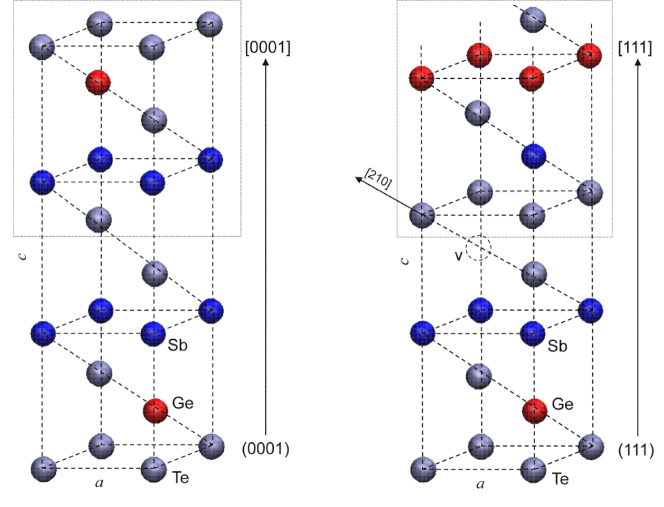
According to the literature, the stacking sequence of the hexagonal cell is made up of 9 layers. Three possible configurations have been proposed, depending on the position of the Sb and the Ge atoms. In an early work Petrov and coworkers [2] proposed the sequence ; more recently, Kooi and de Hosson identified a new stacking where all Sb and Ge atoms exchange their positions [3], while Matsunaga and coworkers suggested that Sb and Te can randomly occupy the same layer, thus resulting in a mixed configuration [4]. Among these configurations, we have adopted that proposed by Kooi and de Hosson, whose total energy is claimed to be the lowest in the computational studies available in the recent literature [12, 13, 19]. As for the fcc structure, the fact that the phase transition occurs easily between hexagonal and cubic GST suggests that the transformation does not imply a large atomic rearrangement, and the two stackings must share a common background.
The unit cell for the hexagonal phase here considered is then made up of 9 atoms and arranged in the stacking sequence , while the fcc structure comes out from shifting the hexagonal sub-unit along the direction to the next crystallographic plane, thus creating a vacancy site () in between. That leads to a unit cell of atoms and vacancies arranged in the stacking sequence repeated three times (figure 1). The experimental values for the cell parameters are: Å, Å for the hexagonal phase [20], and Å [21], corresponding to Å, Å in the equivalent hexagonal system, for the fcc structure. The geometry relaxation resulted in a difference from the experimental data of , for the hexagonal phase, and of , for the fcc phase. Moreover, a slight shift in the position of internal planes is also found. The calculated shrinkage of the parameter is consistent with the adopted LDA approximation, and can also be found in the works of Sun et al. [19] and of Lee and Jhi [12], but contrasts with the results of Sosso et al. [13].
A -point grid for the hexagonal GST and, respectively, a grid for the fcc phase have been used for the self-consistent calculation in order to determine the ground-state configurations for the two systems at hand. The whole relaxation process for the hexagonal structure took around 2 days on a 8-processor Linux cluster. Due to the intrinsically higher structural complexity, the computational load for the fcc cell proved to be times higher.
As the material optical response is due to transitions within and between valence and conduction bands, the first step towards its calculation, once the ground state is known, involves computing the eigenfunctions and eigenvalues also for the conduction band. A uniform grid of was used at this stage for both the hexagonal and the fcc cases. As the optical response strongly depends on the transitions to the conduction band, introducing a dense grid in the calculations increases the accuracy of the calculations themselves. The equations used to build the complex dielectric tensor are reported in the appendix.
The last part of the present investigation concerns the vibrational modes. To this aim we have adopted the DFPT approach [22] provided by the Quantum Espresso package. This method sidesteps the need of constructing a superlattice typical of the standard frozen-phonon framework [23], and allows one to calculate the phonon-dispersion relation. The calculation breaks into three steps, namely, (i) computing the ground-state charge density for the unperturbed system, (ii) evaluating the phonon frequencies and the dynamical matrices at a given -vector and, (iii) transforming the dynamical matrices back in the real space. The calculation of the ground-state charge density is performed by the self-consistent procedure described earlier. The parameters used in step (i) (cutoff energy, convergence threshold, Gaussian smearing, and so on) are the same as those of the band-structure calculation. However, a -dense -point grid has been adopted here. The phonon calculation is performed with a -vector grid.
3 Results and Discussion
3.1 Band Diagram and Density of States
In figures 2 and 3 we report the electronic band structures along high-symmetry lines around the top of the valence band (VB) and the bottom of the conduction band (CB). The DOS is also shown. The actual calculation was performed in an energy interval larger than that shown, this proving the existence of a few deeper bands. Apart from the extension of the band gap that will be discussed later, the shape of the bands compares favorably with the calculations of Yamanaka et al. [24] and, despite the different parametrization of the pseudopotentials, matches very well the results by Lee and Jhi [12], both qualitatively and quantitatively. A preliminary band diagram for the fcc phase has recently been published by some of the authors [25].
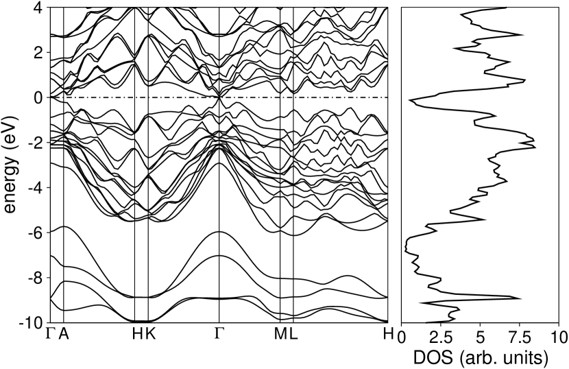
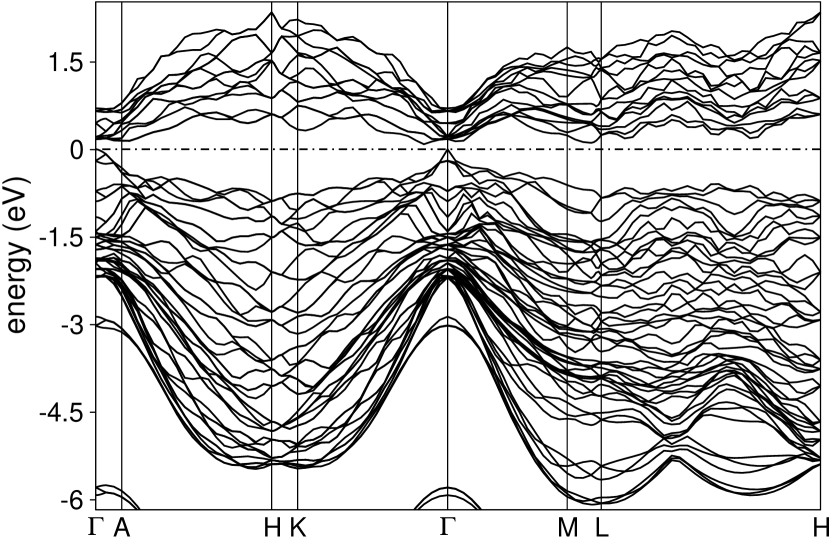
As a result of the simulations, a band gap smaller than what measured in optical experiments (0.5 eV) [8, 26] is found in both cases. More specifically, the hexagonal phase apparently acts as a semi-metal (VB and CB are degenerate at the point), whereas an indirect band gap of about 0.1 eV is found for the fcc phase. This result is consistent in shape with the findings of optical experiments that indicate an indirect bang gap for this phase.
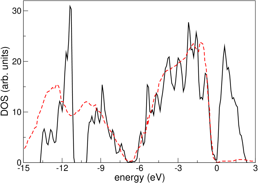
In the recent works of Lee and Jhi [12] and of Sosso et al. [13] a band gap of about 0.2 eV, smaller than the optically-determined one, is found also for the hexagonal phase. The work of Lee and Jhi and that of Sosso et al. do not share the same parametrization of the valence electrons for Te, nor have the same size of the unit cell, but achieve similar results for the band gap. On the other hand, the shape of the bands found in this work is almost the same as that of Lee and Jhi and, once the conduction band obtained by our calculation is shifted towards higher energies, it can be superimposed almost exactly to that of Lee and Jhi. Moreover, apart from high-frequency oscillations probably related to different interpolating schemes, the calculated DOS for the hexagonal phase is consistent with that of Sosso et al. for both the valence and conduction bands. The same situation also holds true for the fcc phase with respect to experimental data (figure 4). One difference between this result and those of Sosso et al. and of Lee and Jhi relies on the approximation of the exchange-correlation potential (LDA instead of the generalized-gradient approximation). The use of different parametrizations for the pseudopotentials and the exhange-correlation term results in different lattice constants and band gap values. Nevertheless, the discrepancies in the band gap among this work and the two references above are well within the intrinsic procedure error [28].
The underestimation of the band gap is a well known effect of the DFT calculation and can be corrected by the GW approach and the Bethe-Salpeter equation, to take into account many-body effects [29].
Despite this limitation, DFT is able to reproduce trends, such as a variation in the band gap due to structural changes. This is the case of the slight increase in the band gap found in the transition from the hexagonal to the fcc phase. In fact, the stoichiometry of the fcc phase implies that 20% of the lattice positions are represented by vacancies, situated between two well-defined sub-units of the unit cell. Due to the increased distance, the Te-Te bond of the fcc structure is much weaker than that of the hexagonal counterpart. When a melt is quickly undercooled to the amorphous state, the number of weak bonds found in the final structure is quite large, and rings and structural defects are also found [6, 7, 30]. According to the capability of predicting trends of the DFT calculations, since the entropy grows from the hexagonal to the fcc crystal and from the fcc phase to the amorphous one, a wider band gap is expected for the latter, consistently with optical determinations. For these reasons, the obtained bands are suitable for being incorporated into a transport simulation scheme that takes into account all of the material phases, including the amorphous one.
The second effect leading to the underestimation of the band gap is that the measured band gap depends on the position of the Fermi level. For a -type degenerate semiconductor such as crystalline GST [31], the Fermi level is inside the valence band. As a consequence, for an interband optical transition to occur, a photon must be absorbed having an energy larger than the difference between the band edges. Therefore, the optical band gap of a degenerate semiconductor is larger than the electronic band gap (Burstein-Moss shift [32]). A proof that the crystalline GST is a -type degenerate semiconductor comes from the experiments based on the Hall effect. Indeed, to explain the temperature-dependence of the Hall coefficient it is necessary to assume that the Fermi level for the hexagonal GST is about 0.1 eV lower than the valence band edge [8].
3.2 Optical Properties
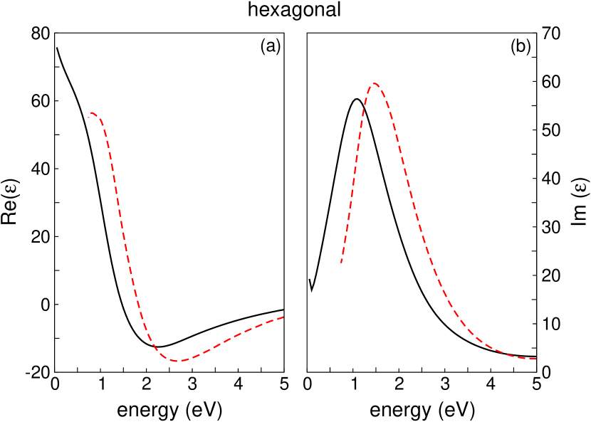
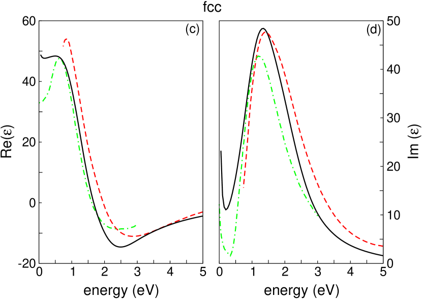
The calculated real and imaginary parts, and , of the dielectric function of the two phases are shown in figure 5. They are superimposed with the corresponding experimental relations found in the literature [8, 26, 31]. To properly compare the experimental and theoretical data it is necessary to remind that the dielectric function depends on the band gap. The detailed expressions are shown in the appendix. As the DFT calculation underestimates the band gap, we expect that the calculated dielectric function be rigidly shifted on the energy axis toward the lower energies with respect to the experimental one. This indeed happens, and the horizontal offset found between the experimental and theoretical curves (approx. 0.5 eV) complies with such an interpretation. Since DFT does not take into account many-body effects, excitonic effects have been ignored.
The calculated and experimental refractive index , along with the extinction and absorption coefficient , are also compared (figure 6). Similar calculations for the absorption coefficient are available in the literature [12] for the hexagonal phase, though using a different set of pseudopotentials, and are reported in figure 6(e) for a straightforward comparison. As , and are calculated through and , the same reasons accounting for the discrepancies in the dielectric function still hold true. However, we stress a better matching for the fcc data, which may be an evidence of a calculated band gap closer to the experimental one.
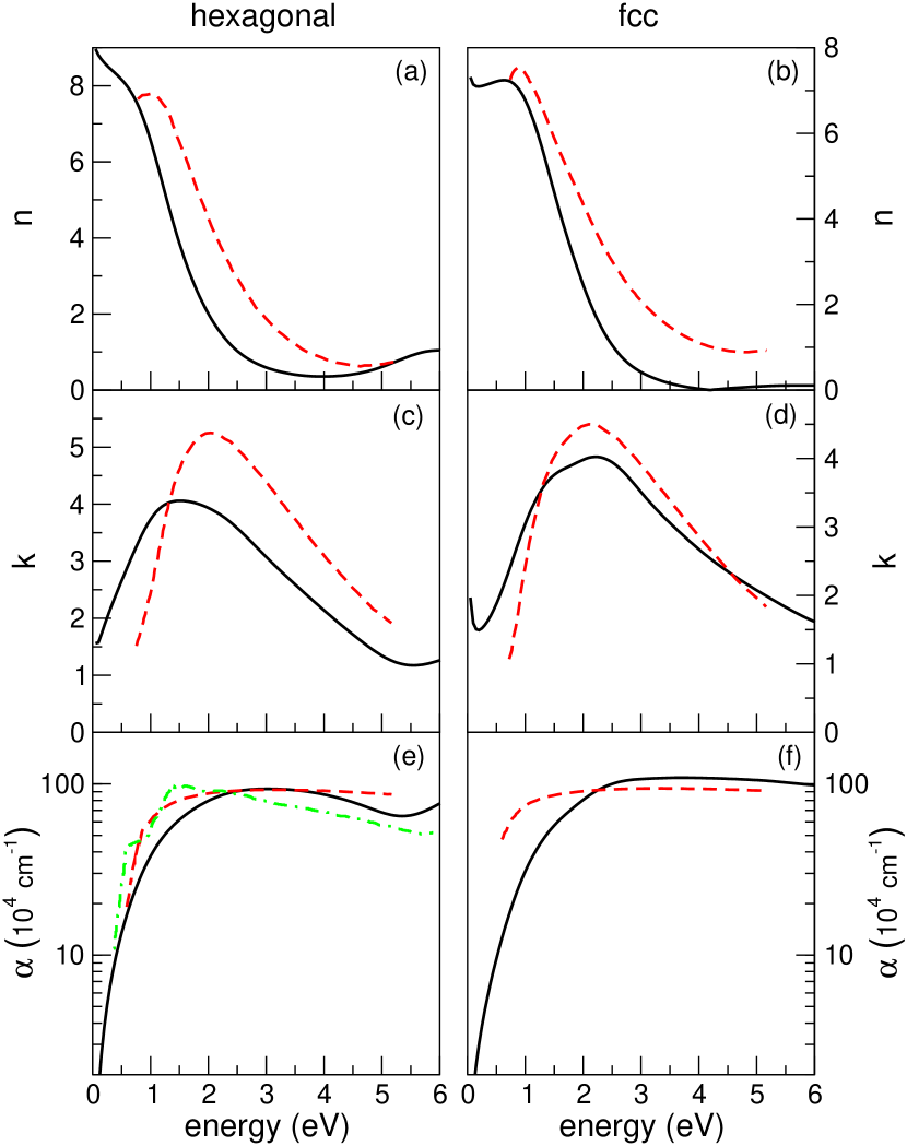
It is also worth noting that the optical determination of the band gap requires extra calculations. In fact, as shown in the two bottom panels of figure 6, the absorption coefficient can be measured accurately only in a range of energies that is somewhat larger than the optical band gap. As a consequence, the intercept of the experimental curve with the energy axis must be found by extrapolation. This is typically done by assuming a power-like relation [33]
| (1) |
where denotes the photon energy, the optical band gap, and the exponent equals for an indirect band gap. The value of is determined by the intersection of with the energy axis . However, equation (1) relies on a model which simplifies the calculated bands. This introduces another error source in the determination of the band gap, that adds to the ones discussed earlier.
To better compare numerical results with experiments it is also useful to calculate practically measurable quantities such as the optical transmission and reflection . As in most cases GST samples are available as thin films on substrates, it is necessary to account for the dependence of and on the film thickness. Two GST samples with significantly different thicknesses have been prepared and tested for each phase. They were sputter-deposited on glass slides and then annealed in an argon atmosphere for minutes at C (for the fcc phase) or C (for the hexagonal phase). Following the procedure described elsewhere, [26] the optical transmission and reflection were measured at an incidence angle of and , respectively. The optical thickness, estimated by fitting the data to the previously-obtained optical constants, is 15 and 240 nm for the fcc samples, and 12 and 240 nm for the hexagonal samples.
The dependence of , on thickness has been evaluated numerically by solving the optical equations [34] for a normally-incident light on a thin layer on top of a thick glass substrate with and .
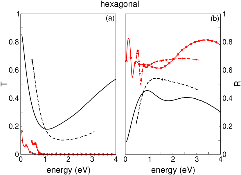
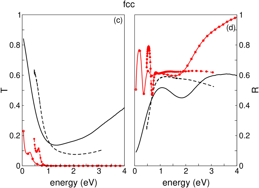
The results are reported in figure 7. In both cases the transmission scales down and, conversely, scales up with thickness, as should be. Interference fringes are present in the spectra near or below the optical band gap, since multiple reflections occur inside the film and interfere with each other. Once again, the calculated data suffer from the underestimation of the band gap, but the comparison is quite satisfactory, especially for the thick samples.
3.3 Phonon calculation
The calculation of the full dispersion spectrum is a rather demanding task, and very strict convergence criteria are often required. Therefore, we have limited our analysis to the DOS with the aim of calculating the speed of sound and heat capacity of the material, which can be directly compared with experimental data. More details about the complete phonon spectrum are left to future work. The phonon DOS for the hexagonal GST is shown in figure 8(a). The general tendency of chalcogenides to have very low phonon frequencies in the range of few tens of meV [13] is confirmed by our findings. The analogous calculation for the fcc phase resolved into unstable results and a number of imaginary frequencies were also found with any reasonable set of the simulation parameters cited in section 2. This calculation is omitted from the present publication; however this may prove once more that the fcc structure is metastable.
The obtained speed of sound along the three orthogonal directions is around nm/ps, nm/ps and nm/ps for the two transverse and the longitudinal branch, respectively. The last value compares well with the experimentally estimated nm/ps reported in the literature [35]. In the high temperature limit, the speed of sound can be exploited to determine the lattice contribution to the minimum thermal conductivity of the material:
| (2) |
where cm-3 is the atomic density, and is the Boltzmann constant. The lattice contribution to the minimum thermal conductivity is W/(m K), a lower value than those observed in experiments for the hexagonal phase.
However, this result must be interpreted with care, and three aspects deserve attention. First, it should be pointed out that the hexagonal phase is the only stable phase existing at high temperatures (typically above 600 K), and data often refer to that range.
Next, according to Reifenberg and co-workers [36], the GST thermal conductivity depends also on the film thickness. For the hexagonal phase they found a decrease from W/(m K) for a -nm thick sample to W/(m K) for a -nm thick sample.
Finally, the carrier density in hexagonal crystalline GST is relatively large and electrical carriers also contribute to the heat transport. Experiments have estimated that the electrical contribution is roughly equivalent to the lattice contribution [37], thus leading to an overall conductivity about twice that of calculated above. Thus, taking into account these remarks, is consistent with the phonon contribution in the experiments.
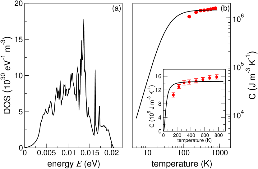
A further confirmation about the validity of the reported DOS comes from a comparison of the calculated heat capacity of GST with that experimentally-determined by Kuwahara and co-workers [38]. Let be the energy of the phonon; the heat capacity can be calculated from the simulated phonon DOS by means of:
| (3) |
where is the Bose-Einstein distribution function, and is the temperature. The calculated and experimental data are reported in figure 8 up to 870 K, which corresponds to the approximate melting temperature of GST. According to Kuwahara, the experimental heat capacity slightly increases in the high-temperature region, as the result of structural relaxation of point defects. However, the integral in (3) includes only the lattice contribution to heat capacity, and thus predicts a saturating value in the classical limit at high temperature. Nevertheless, the comparison is good, and calculated data are consistent with experiments in the whole range examined. In addition, these calculations provide an estimate of the heat capacity of hexagonal GST in the temperature range where experimental data are unavailable ( K).
4 Conclusion
In this paper, we reported the electronic and optical properties for the hexagonal and face-centered cubic phases of the Ge2Sb2Te5 chalcogenide.
The electronic band diagram and DOS were calculated using the density functional theory combined with planes waves, norm-conserving pseudo-potentials and the local density approximation implemented in the code Quantum Espresso. The band diagram and DOS for the hexagonal phase are in good agreement with those reported in the literature. Even though DFT equations are known to underestimate the band gap, the shape of the bands confirms the existence of an indirect band gap for the fcc phase, and the DOS of the latter correctly compares to previously published data. The calculation also showed a tendency of the band gap to increase with respect of the degree of disorder of the cell. This result makes the band diagrams suitable to be used in transport simulations that describe the electrical behaviour of GST.
The dielectric function was obtained implementing the Drude-Lorentz expression and the Kramers-Kronig relationships. Furthermore, the refractive index, the extinction and absorption coefficients were derived from the Maxwell model. By incorporating these functions into equations including multiple internal reflection, the optical transmission and reflection for a thin chalcogenide film deposited on a glass substrate were calculated and then compared to experiments. Most of the differences in the comparison can ascribed to the underestimation of the band gap.
Moreover, the density functional perturbation theory allowed us to calculate also the phonon DOS for the hexagonal phase. The analysis of the acoustic modes for the hexagonal phase led to reasonable values for both the speed of sound and the minimum thermal conductivity at room temperature. The heat capacity from 5 K up to the melting temperature is also presented, in good agreement with experimental data at high temperature, and providing insight into the low temperature range ( K) where data are unavailable.
Appendix – Derivation of the optical properties from the band diagram
In the framework of band theory without electron-hole interaction, the dielectric tensor is defined as
| (4) |
with . In (Appendix – Derivation of the optical properties from the band diagram) , and are the electron charge and mass, and the volume of the lattice cell, respectively; are the eigenvalues of the Hamiltonian and is the Fermi distribution function accounting for the band occupation. Letting be the plasma frequency with standing for the number of electrons per unit volume, and , the imaginary part of the dielectric tensor is given by the following Drude-Lorentz expression:
| (5) |
where the original sum over and of (Appendix – Derivation of the optical properties from the band diagram) has been split into two terms, the former accounting for valence-to-valence (or conduction-to-conduction) intraband transitions (), the latter standing for transitions from states belonging to the valence band (index ) to states belonging to the conduction band (index ). In the summands, the squared matrix elements are weighted by a smearing coefficient ( or ), and by a factor depending on the Fermi distribution function for interband transitions, or on its derivative for the intraband contribution. Considering that the derivative is substantially zero except in the region close to the Fermi level, the dielectric tensor is dominated by interband transitions, as expected. Nevertheless, a few states near the top of the valence band can be empty due to thermal excitations and, conversely, a small amount of states in the conduction band are occupied. As a consequence, a number of intraband transitions occur, that are described by the first summand of equations (5) and (6). Accounting for such transitions is useful to better reproduce the experimental behaviour.
In order to keep the Drude-Lorentz approximation valid, the two smearing coefficients and must be small, even though not vanishing. For the case described in the text they were treated as fitting parameters and both set to 1.0 for the hexagonal phase and to 0.8 and 0.3, respectively, for the fcc phase.
The real part of the dielectric tensor is then calculated applying the Kramers-Kronig relationship to (5):
| (6) |
The squared matrix elements reveals the tensorial nature of and are defined as follows:
| (7) |
where is a factor of the single particle Bloch function obtained by the Kohn-Sham DFT calculation, and is the momentum operator along the direction.
In a principal system, the off-diagonal elements of the dielectric tensor are zero and, for perfectly isotropic materials, the diagonal elements are equal. For the two systems considered here, only two eigenvalues out of three are equal. In order to compare results with experimental data where isotropy is assumed, the eigenvalues of the dielectric tensor have been averaged to obtain a unique function.
The refractive index , the extinction coefficient and the absorption coefficient are calculated by means of the Maxwell model through the following relationships:
| (8) | |||||
| (9) | |||||
| (10) |
where the symbols and without superscripts represent an average function determined as described above.
References
References
- [1] Ovshinsky SR 1968 Phys. Rev. Lett.21 1450
- [2] Petrov II, Imamov RM and Pinsker ZG 1968 Sov. Phys. Crystallogr. 13 339
- [3] Kooi BJ and de Hosson JTM 2002 J. Appl. Phys.92 3584
- [4] Matsunaga T, Yamada N and Kabota Y 2004 Acta Crystallogr.B 60 685
- [5] Kolobov A, Fons P, Frenkel AI, Ankudinov AL, Tominaga J and Uruga T 2004 Nat. Mater. 3 703
- [6] Akola J and Jones RO 2007 Phys. Rev.B 76 235201
- [7] Caravati S, Bernasconi M, Kühne TD, Krack M and Parrinello M 2006 Appl. Phys. Lett. 91 171906
- [8] Lee BS, Abelson JR, Bishop SG, Kang DH, Cheong B and Kim KB 2005 J. Appl. Phys.97 093509
- [9] Pirovano A, Lacaita AL, Benvenuti A, Pellizzer F and Bez R 2004 IEEE Trans. Electron Dev. 51 452
- [10] Ielmini D and Zhang Y 2007 J. Appl. Phys.102 05451
- [11] Buscemi F, Piccinini E, Brunetti R, Rudan M and Jacoboni C 2009 J. Appl. Phys.106 103706
- [12] Lee G and Jhi SH 2008 Phys. Rev.B 77 153201
- [13] Sosso GC, Caravati S, Gatti C, Assoni A and Bernasconi M 2009 J. Phys.: Condens. Matter21 245401
- [14] Giannozzi P et al. 2009 J. Phys.: Condens. Matter21 395502
- [15] Perdew JP and Zunger A 1981 Phys. Rev.B 23 5048
- [16] Gonze X and Stumpf R and Scheffler M 1991 Phys. Rev. Lett.44 8503
- [17] Do GS, Kim J, Jhi SH, Louie SG and Cohen ML 2010 Phys. Rev.B 82 054121
- [18] van Lenthe E, Snijders JG and Baerends EJ 1996 J. Chem. Phys.105 6505
- [19] Sun Z, Zhou J and Ahuja R 2006 Phys. Rev. Lett.96 055507
- [20] Friedrich I, Weidenhof V, Njoroge W., Franz P and Wuttig M 2006 J. Appl. Phys.87 4130
- [21] Park YJ, Lee JY, Youm MS, Kim YT and Lee HS 2005 J. Appl. Phys.97 093506
- [22] Baroni S, de Gironcoli S, Dal Corso A and Giannozzi P 2001 Rev. Mod. Phys.73 515
- [23] Parlinski K, Li ZQ and Kawazoe Y 1997 Phys. Rev. Lett.78 4063
- [24] Yamanaka S, Ogawa S, Morimoto I and Ueshima Y 1998 Japan. J. Appl. Phys.37 3327
- [25] Piccinini E, Tsafack T, Buscemi F, Brunetti R, Rudan M, Jacoboni C 2008 Proc. of the 2008 Int. Conf. on Simulation of Semiconductor Processes and Devices (SISPAD) (Hakone, Japan) (Piscataway, NJ: IEEE) 229
- [26] Shportko K, Kremers S, Woda M, Lencer D, Robertson J and Wuttig M 2008 Nat. Mater. 7 653
- [27] Kim JJ, Kobayashi K, Ikenaga E, Kobata M, Ueda S, Matsunaga T, Kifune K, Kojima R and Yamada N 2007 Phys. Rev.B 76 115124
- [28] Gygi F and Baldareschi A 1989 Phys. Rev. Lett.62 2160
- [29] Onida G, Reining L and Rubio A 2002 Rev. Mod. Phys.74 601
- [30] Hegedüs J and Elliot SR 2008 Nat. Mater. 7 399
- [31] Lee BS and Bishop SG 2009 Optical and Electrical Properties of Phase Change Materials Phase Change Materials (Science and Applications) Ed S Raoux and M Wuttig (New York, NY: Springer)
- [32] Moss TS 1959 Optical Properties of Semiconductors (London, UK: Butterworths Scientific Publications Ltd)
- [33] Mott NF and Davis EA 1979 Electronic Processes in Non-Crystalline Materials 2nd ed (Oxford: Clarendon Press) p. 273
- [34] Tsu DV 1999 J. Vac. Sci. Technol. A 17 1854
- [35] Lyeo HK, Cahill DG, Lee BS, Abelson JR, Kwon MH, Kim KB, Bishop SG and Cheong B 2006 Appl. Phys. Lett. 89 151904
- [36] Reifenberg RP, Kim S, Gibby A, Zhang Y, Panzer M, Pop E, Wong S, Wong HS and Goodson KE 2007 Appl. Phys. Lett. 91 111904
- [37] Yang Y, Li CT, Sadeghipour SM, Dieker H, Wuttig M and Asheghi M 2006 J. Appl. Phys.100 024102
- [38] Kuwahara M, Suzuki O, Yamakawa Y, Taketoshi M, Yagi T, Fons P, Fukaya T, Tominaga J and Baba T 2007 Japan. J. Appl. Phys.46 3909