All-optical active plasmonic devices with memory and power switching functionalities based on -near-zero nonlinear metamaterials
Abstract
All-optical active plasmonic devices are of fundamental importance for designing efficient nanophotonic circuits. We theoretically propose and numerically investigate an active plasmonic device made up of a nonlinear -near-zero metamaterial slab of thickness smaller than nanometers lying on a linear -near-zero metamaterial substrate. We predict that, in free-space coupling configuration, the device, operating at low-intensity, would display plasmon mediated hysteresis behavior since the phase difference between the reflected and the incident optical waves turns out to be multi-valued and dependent on the history of the excitation process. Such an hysteresis behavior would allow to regard the proposed device as a compact memory unit whose state is accessible by measuring either the mentioned phase difference or the power, which is multi-valued as well, carried by the nonlinear plasmon wave. Since multiple plasmon powers comprise both positive and negative values, the device would also operate as a switch of the plasmon power direction at each jump along an hysteresis loop.
pacs:
73.20.Mf, 42.79.Vb, 81.05.ZxI INTRODUCTION
Confinement and steering of optical radiation at nanometer scale are fundamental issues of modern nanophotonics and a dominant role is played by surface plasmon polaritons Bronge ; Shala1 (SPP) which are collective electron density oscillations coupled to external electromagnetic waves Raethe existing at metallo-dielectric interfaces. The surface charge oscillations merge the dielectric evanescent waves with the metal exponentially decaying fields so that SSPs are surface modes tightly confined at the interface, a fundamental ingredient for the miniaturization of optical components down to the sub--nm-size regime Barnes . Aimed at designing photonic circuits, controlling SPPs flow is an important topic and various waveguiding schemes have been proposed Ebbese ; Gramot together with a plenty of passive plasmonic devices encompassing mirrors Ditlba , lenses Liuuu1 , interferometers Ziaaaa , splitters Bozhev and resonators Minnnn . Although passive plasmonic devices can provide some of the essential components for signal processing, an efficient photonic circuitry amenable to be integrated with nanoscale electronics evidently requires externally driven (active) plasmonic devices MacDon and plasmonic emitters Koller ; Hryciw , detectors Tanggg ; Neuten and plasmon lasers Oulton ; Kwonnn have been considered. In order to manipulate the plasmon flow along the path between the source and the detector, the dielectric refractive index near the metal surface has to be externally controlled and this can be done through an electro-optic medium to obtain electrically-driven plasmonic modulators Caiiii . Electro-optic methodology is particularly intriguing since both optical and electrical signals can in principle be processed and interconnected on the same circuit board. Another viable way to actively affect plasmon propagation consists in employing a nonlinear dielectric medium with a large Kerr nonlinearity and this has lead to the observation of plasmon mediated optical bistability Wurtz1 and all-optical modulation of surface plasmon polaritonic crystal transmission Wurtz2 . The main drawback to the use of the Kerr nonlinearity is that the nonlinear response is generally weak and, even if SSPs are accompanied by a large field enhancement, the required optical intensities are very large. For this reason, even though there is a considerable research effort in nonlinear plasmonics Palomb ; Shaooo ; Yinnnn ; Marini , an efficient nonlinear active plasmonic device has not been devised yet.
The research interest in surface plasmons has been further increased by the availability of metamaterials which are artificially structured materials whose underlying subwavelength constituents are suitably tailored to allow the engineering of the overall medium electromagnetic response. As an example, it has been recently suggested that the flow of SPPs on metallo-dielectric interfaces can be efficiently (and passively) controlled by exploiting the metamaterial based transformation optics technique to devise the optical parameters of the dielectric medium Huidob ; Liuuuu .
The investigation of metamaterial nonlinear properties is particularly important in that it can lead to overcoming one of the fundamental limit of nonlinear optics, the fact that most of the optical materials have a relatively weak nonlinear response. The main idea is that the local electromagnetic fields of the inclusions in the metamaterial can be much larger than the average value of the field thus producing an enhancement of the nonlinear response Pendr3 . Following a very different route, it has recently been proposed that an extremely marked nonlinear behavior can be observed, instead of by enhancing the nonlinear response, by substantially reducing the metamaterial linear dielectric permittivity Ciatt1 and this strategy has allowed to predict self power-flow reversing of an optical beam Ciatt2 and transmission optical bistability of a slab of sub-wavelength thickness at very low optical intensities Ciatt3 ; Ciatt4 . It is worth noting that, as opposed to standard media where nonlinearity requires macroscopic propagation lengths (greater than a centimeter) to produce an all-optical manipulation, -near-zero nonlinear metamaterials dramatically affect light just at their free-space interface (as discussed in Ref.Ciatt3 ) and therefore they are candidates to play a pivotal role in designing nanophotonic nonlinear active devices, one of which is discussed in the present paper.
In this paper we theoretically investigate a nanoscale all-optical active plasmonic device which, operating at low optical intensities and being integrable in a photonic circuit, could be used both as plasmonic memory unit and as a device able to switch the direction of the power carried by a surface plasmon wave. The system basically consists of a few tens of nanometers thick slab of a nonlinear Kerr metamaterial lying on a linear metamaterial substrate, the nonlinear and linear medium having very small dielectric permittivities of opposite signs. Since the substrate permittivity is much smaller than one, the critical angle to achieve phase-matching between free-space waves and surface plasmons is rather small (of the order of few degrees) so that total reflection of a free-space plane wave impinging onto the nonlinear slab surface is easily observed and it is accompanied by the excitation of a nonlinear plasmonic wave at the slab-substrate interface. The small value of the slab permittivity allows the nonlinearity to produce a rather complex hysteresis behavior (in analogy of the transmissivity hysteresis described in Ref.Ciatt3 ) which is easily detectable by measuring the phase difference between the reflected and the incident optical wave. Therefore the system can be regarded as a nanoscale memory unit on a board whose state is easily read out through a reflection experiment. Note that optical bistability from surface plasmon excitation has been investigated employing metal-coated prisms in the attenuated total reflection (ATR) or Kretschmann geometry in the presence of a nonlinear dielectric Wysinn ; Hicker ; Zhouuu but these setups are not easily scaled down to be integrated in a photonic circuit due to the macroscopic prism dimension, a difficulty completely avoided by the device discussed in this paper. The nonlinear surface plasmon carries optical power along the slab-substrate interface and, due to the chosen extreme nonlinear regime, the overall plasmon power can be both parallel and anti-antiparallel to the plasmon wave-vector, an exotic situation generally not occurring in the presence of linear materials with positive magnetic permeability. The total plasmon power follows the hysteresis slab behavior and therefore the power direction can be switched simply by changing either the input optical intensity or the incidence angle to force the system to jump to a different hysteresis state.
II Nonlinear Plasmonic Device
We start by considering the plasmonic device consisting in a slab of thickness lying on a substrate as reported in Figure 1a. Here we consider monochromatic electromagnetic radiation whose free-space wavelength is . The slab is a nonlinear Kerr metamaterial with a very small linear dielectric permittivity and a viable way to produce this artificial medium is to repeat along the -axis nonlinear metal and dielectric layers of thickness and , respectively. If both thicknesses are much smaller than , radiation experiences a uniform electromagnetic response obtained by averaging both the linear permittivities and and the nonlinear Kerr coefficients and Ciatt1 .
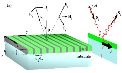
Therefore, since metal layers have negative dielectric permittivity, it is possible to choose and in such a way that the slab average dielectric permittivity is (-near-zero metaterial Silver ; Aluuuu ) and . Note that we are considering a real permittivity and this can be achieved by using dielectric layers with gain to balance the metal losses Ramak2 . The substrate is a linear metamaterial with dielectric permittivity and it can be manufactured either by means of the same technique employed for the slab with linear layers or by exploiting the method discussed in Ref.Zengg1 ; Zengg2 , consisting in dispersing silver coated spherical semiconductor quantum dots (with optical gain) in a homogeneous host material whose permittivity can be externally tuned. As reported in Figure 1a, an incident plane wave (i) is made to impinge onto the slab-vacuum interface (the plane ) with incidence angle and with the complex electric field belonging to the plane of incidence (parallel to the plane ) which is parallel to the slab layers. A nonlinear plasmon mode localized at the slab-substrate interface (the plane ) can be excited only if the incident plane wave is phase-matched with the substrate evanescent waves and this happens if is greater than the critical angle degrees. Therefore, for , total reflection occurs since both and are real and consequently (where is the dimensionless electric field magnitude), the reflection solely yielding a phase difference between the reflected and incident waves given by
| (1) |
As schematically sketched in Figure 1b, total reflection produces a nonlinear localized mode at the interface which is a transverse magnetic (TM) field (see Appendix A). Evidently, the energy flow is purely along the -direction since the Poynting vector is everywhere and hence, the total power per unit length carried by the nonlinear wave is
| (2) |
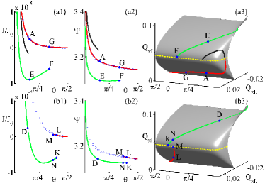
We have numerically evaluated nonlinear plasmon modes (see Appendix A) for a number of excitation states (, ) characterized by the incidence angle and the incident plane wave amplitude and, for each mode, we have evaluated the phase difference from Eq.(1) and the power per unit length from Eq.(2). In Figure 2 we report the evaluated and along four possible ways (denoted with a, b, c and d) of varying the parameters (, ). In situations (a) and (b) the amplitude is hold fixed with and , respectively and the incidence angle is varied in the range whereas in situations (c) and (d) the angle is hold fixed with and , respectively and the amplitude is varied in the range . For comparison purposes, in each panel of Figure 2 reporting or we have also plotted (blue empty circles curves) the corresponding linear quantities i.e. or as evaluated for a linear slab of dielectric permittivity . Note that, in each situation reported in Figure 2, both and are multi-valued function of the excitation parameters or, more precisely, this quantities generally assume more than one value for a given excitation state (, ). This implies that the considered system displays multistability controllable through the incidence angle and the input optical intensity, and detectable by measuring or . From Figure 2, it is evident that the values of and lie on at most three different branches (red, green and black lines) and, most importantly, that the branches presents points at which they abruptly stop (see, e.g., state of panels a1 and a2, states and of panels b1 and b2, state of panels c1 and c2 and states and of panels d1 and d2). The fact that different branches abruptly stop and that they are not mutually continuously connected imply that the multistability discussed in this paper is supported by a mechanism fundamentally different from that (feedback effect) yielding the standard optical bistability.
III Plasmonic Multistability
In order to discuss the physical mechanism supporting the obtained multi-stable phenomenology it is convenient to consider the electromagnetic matching conditions at the interface which yield
| (3) |
where and are the values of the and dimensionless electric field components at the interface on the slab side (see Appendix A). For and assigned, Eq.(3) provides the allowed values of (electric field component normal to the slab-substrate interface). Note that for a linear slab the first term of Eq.(3) reduces to this implying that only one value of is allowed. In the four panels a3, b3, c3 and d3 of Figure 2 we plot the surface obtained from Eq.(3) in the range (without loss of generality) and we note that such surface is folded. This implies that, due to the effect of the nonlinearity, the electromagnetic boundary conditions generally allow more than one electromagnetic configuration at a given and plasmon amplitude , the various configurations having different values of . Each point of the surface corresponds to a nonlinear plasmon mode and therefore, in panels a3, b3, c3 and d3 of Figure 2, we have also reported the various state curves of plasmon modes used to evaluate and of the corresponding panels in the Figure, using the colors to establish the correspondence. The red branches of both and of Figure 2 practically coincide with their linear counterparts (the empty circles curves) apart from the region close to the breaking points so that we conclude the green branches to be of pure nonlinear origin and arising from the surface folding which is therefore the crucial element producing the multistability of and . It is worth noting that folding takes place if the surface admits critical points where the partial derivative of Eq.(3) with respect vanishes, i.e.
| (4) |
which represents the curve of critical points reported with a dashed yellow line in panels a3, b3, c3 and d3 of Figure 2. From Eq.(4) we readily deduce that critical points can appear only if the field amplitudes and are comparable with and this physically means that linear and nonlinear contributions to the overall electromagnetic slab response must be comparable. This is an extreme nonlinear condition Ciatt1 made here possible by the fact that the slab permittivity is much smaller than one. It is worth noting that, in a conventional nonlinear medium where the permittivity is of the order of unity, the above folding would required an optical intensity so large to effectively prevent the whole discussed phenomenology to take place. We therefore conclude that the multistability discussed in this paper can uniquely be observed by means of -near-zero nonlinear metamaterials. To get further physical insight, note that the constitutive relations yield , so that Eq.(4) coincides with the condition . Therefore the plasmon states below and above the critical curve are characterized by and , respectively and therefore characterized by very different electromagnetic features (the curve of critical point playing the role of a separatrix between the two electromagnetic regimes). This is particularly evident from panel d3 of Figure 2 where states and are just below and above the critical curve, respectively (and hence their electric amplitudes are almost equal at ) and nonetheless their corresponding values of and of panels d1 and d2, respectively, are very different. The existence of two distinct electromagnetic regimes explains both the different values of and along the red and green branches (bistability) and branch breaking since, from Figure 2, it is evident that the points at which the branches of and abruptly stop correspond to a plasmon mode whose and lie just either below or above the yellow critical points curve (state of panels a1, a2 and a3, state and of panels b1, b2 and b3, etc.)
IV Device memory and power switching functionalities
By combining the discussed multistability with the branch breaking it is easy to prove that the considered system displays a complex hysteresis behavior allowing to regard the system as a device with structured memory functionality. Suppose, for example, that the incident plane wave is such that and so that, from panels d1, d2 and d3 of Figure 2, it is evident that a state of the red curve is excited since for the green branch has no corresponding allowed states. By increasing the input intensity (and hence ) the state is reached and surpassed toward the state . Once is reached, if the input intensity is further increased the system has to undergo a sudden jump to the state belonging to the green branch since the red branch stops at . From the state the input intensity can now be decreased toward the state and therefore along such a backward path the attained values of and are different from the forward path, i.e. hysteresis occurs. Evidently, by decreasing the input intensity from the state the system undergoes another jump to reach the state , thus coming back to the red branch and closing the hysteresis loop. The system hysteresis phenomenology is however far more rich since the incidence angle can also be varied. Suppose, for example, that the incident plane wave is such that and so that, from panels b1, b2 and b3 of Figure 2, it is evident that the state belonging to the green branch is excited since the red branch has no corresponding allowed state. If the angle is increased, by reasoning in analogy with the just discussed hysteresis loop, the system can be brought to the state (passing through the state ) and hence forced to jump to the state since is a breaking point of the green branch.
From the system can be driven to by decreasing the incidence angle and eventually it can be forced to jump down to the state thus closing the ”angular” hysteresis loop.
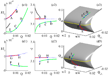
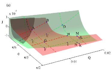
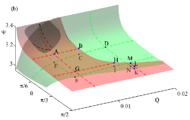
The number of possible hysteresis loops is infinite since and can independently be varied and, in order to provide a global description of the system multistable behavior we report in panels (a) and (b) of Figure 3 the values of and , respectively, for all the possible and in the ranges and . In Figure 3 we also plot, through dashed lines and corresponding colors, all the branches of and considered in Figure 2 together with all the states denoted with capital letters. The surfaces representing and exhibit more than one sheet, each one admitting breaking lines, and the mutual position of the just discussed hysteresis loops G-H-I-F and N-K-L-M is particularly evident. If we choose to operate uniquely with the red and green sheets, it is evident that the system is suitable to record a binary information which can be easily read since a single measure of (or ) allows to know whether a red or a green state is excited. Moreover, the state of the memory unit can be simply altered by driving the system through a breaking line thus forcing a switch of its operating sheet. Note also that the system memory functionality can even be suitably tailored to satisfy external requirements (i.e. specific optical intensities or angles imposed by a possible nearby circuit environment) since, for each plasmonic state, a hysteresis loop can be found which starts and ends at the considered state. Suppose, as an example, that an hysteresis loop containing the red state of Figures 2 and 3 is required. Once the state A is excited, one can increase the field amplitude to reach the state B (which is a red sheet breaking point) and to force the system to jump to the green state . From panel c1 and c2 of Figure 2 or from Figure 3 it is apparent that by solely varying the field amplitude the system can never be brought back to the state A. However, one can drive the system to reach the state E, fix the field amplitude Q and increase the angle to reach the state F (see panel a1 and a2 of Figure 2 or Figure 3) which is a breaking point of the green sheet. Therefore a jump can be induced to make the system reach the red state G and, after reducing the angle, to come back to the initial state A thus closing the hysteresis loop.
In addition to the above discussed multistability and related memory functionality, we note that, from Figures 2 and 3, both positive and negative signs of are allowed. Specifically, the red branches of are always positive whereas the green branches can be both positive and negative. Bearing in mind that the red branches (where they exist) almost coincides with the slab linear behavior, we conclude that the extreme nonlinear regime also introduces the possibility of an overall plasmon power which is antiparallel to the wave-vector. In fact, since the slab and substrate permittivities and are negative and positive, respectively, the Poynting vector is locally antiparallel and parallel to the -direction (which coincide with the plasmon mode wave-vector) and hence the total power can be both positive and negative. For the red branches of of Figure 2 (or 3) the positive contribution to coming from the evanescent field in the substrate overcomes the slab negative contribution thus producing an overall positive . However, the plasmon modes belonging to the green branches are generally characterized by a larger amount of electromagnetic energy stored within the slab since their amplitudes are generally larger than their red counterparts as it is evident from panels a3, b3, c3 and d3 of Figure 2. Therefore the negative contribution to of the green modes can overcome the positive evanescent contribution thus yield an overall negative plasmon power. As an example, states A and E of panels a1 of Figure 2 are excited through the same input intensity and incidence angle and, nonetheless, and . Obviously, for small values of , the extension of the evanescent field thorough the substrate is so large to always yield a positive value of (see the positive portion of the green sheet of in Figure 3a).
The fact that the overall plasmon power, for a given excitation state , can be both parallel or anti-parallel to the wave vector also allows to regard the considered system as a device able to switch the direction of the electromagnetic energy flowing along the slab-substrate interface. In fact, once a state is excited with a given sign of , the energy flow direction switch is easily performed by externally changing the incident plane wave and driving the system through a sheet breaking line whose crossing forces the system to jump to the other sheet where the sign of is generally different from the initial one.
V Device feasibility and design
The feasibility of the above described active plasmonic device is evidently related to the actual availability of both slab and substrate metamaterials exhibiting the above mentioned features. In order to prove that such media can be actually synthesized, we have chosen nm, nm, nm, , , and . The parameters of medium coincide with those of silver Palikk , characterized by a very large nonlinear susceptibility YangGu , with the imaginary part of the permittivity corrected by the layer size effect (since nm) CaiSha . Medium is a linear dielectric with gain (to compensate the metal losses) and its permittivity can be achieved, for example, by embedding, in a polymer background, a bi-dimensional array of colloidal II-VI quantum dots which are properly electrically or optically pumped Fuuuuu through ultra-violet light. The value of here considered is obtained through the Maxwell Garnett mixing rule where and Fuuuuu are the background polymer and quantum dots permittivities, respectively and is the quantum dots volume filling fraction; besides both the polymer and the quantum dots have nonlinear susceptibility much smaller than so that the requirement is assured. Note that, even though the actual fabrication of the considered ultra-small structure is hindered by the very small thickness/width (i.e. ) ratio of the metallic grooves, the required array of metallic nanowires can be manufactured through the general method of Superlattice Nanowire Pattern Transfer (SNAP) MeloshB ; JungJoh ; Martinez which is a novel deposition technique particularly suitable for producing ultrahigh-density arrays of aligned metal and semiconductor nanowires and nanowire circuits. Once the array of silver nanowires is deposited onto the substrate, the vacancies between the metallic grooves can be filled with the required quantum dots dispersed in a suitable liquid monomer (by using, for example, the standard spin-deposition process) which can be eventually polymerized through UV curing. The effective (average) permittivity and nonlinear susceptibility of the considered sample are and . As far as the substrate, we choose here to exploit the just proposed scheme of dispersing silver (for which ) coated spherical semiconductor quantum dots (the same colloidal II-VI quantum dots as in the slab for which ) in a homogeneous host material (for which ). Exploiting the electrostatic treatment of Ref. Zengg1 and choosing for the fraction of the total particle volume occupied by the inner quantum dot core we obtain for the effective permittivity of the overall inclusion . Exploiting the standard Maxwell Garnett mixing rule and choosing for the volume filling fraction of the inclusions dispersed in the hosting matrix, we obtain for the effective dielectric permittivity of the substrate .
VI Full-wave simulations
In order to test the behavior of the above discussed active plasmon device we have performed 3D full-wave simulations by means of a finite-element solver (see Appendix B) in which we have used the numerical values of the parameters just chosen in the above structure design. In panel (a) of Figure 4 we report the comparison between the phase difference evaluated through full wave simulations (blue circles) for and and the corresponding phase difference of panel (c2) of Figure 2 (red and green solid lines).
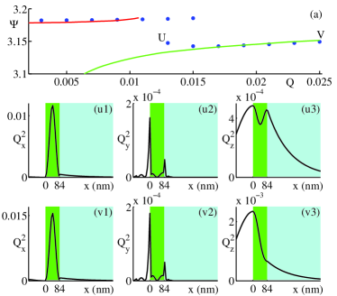
We note that full-wave simulations confirm the existence of the above discussed multistability and branch breaking. For values of far away from the breaking value , full-wave simulations reproduces the predictions of the homogenized approach. On the other hand, discrepancies appear for and, specifically, the breaking point of the upper branch predicted by the full-wave simulations is at instead of of the homogenized theory. The origin of the discrepancies and of the breaking point shift is due to the existence of a further plasmonic resonance arising from the fact that a transverse magnetic plane wave (polarized in the plane, see Figure 1a) is made to impinge onto a metallo-dielectric medium layered along the -direction. Therefore an additional component of the electromagnetic field of plasmonic origin arises thus departing the layered medium behavior from that of its homogeneous counterpart. In order to support this reasoning we plot in panels (u1), (u2) and (u3) and panels (v1), (v2) and (v3) of Figure 4, the profiles of the squared dimensionless electric field components as a function of corresponding to the states and reported in panel (a), respectively. Such squared electric field profiles have been evaluated near the metallic-dielectric interface () where the additional plasmonic states are mainly localized. The state does not display significant discrepancies between full-wave simulations and homogenized approach prediction (see panel (a) of Figure 4) since, as it is evident from panels (v1), (v2) and (v3) of Figure 4, both the and electric field components are much larger than the component. On the other hand, the discrepancy accompanying the state are due to the fact that the electric field component of panel (u2) is comparable with the component of panel (u3).
The intensity of the incident plane wave is which, for the amplitude range (where multistability occurs for ) and for the above effective nonlinear susceptibility , yields , which are intensities smaller than those normally required for observing the standard optical bistability. However it is evident that the smaller the smaller the intensity required for observing the device multi-stable behavior so that very smaller intensity thresholds (of the order of ) are very likely to be attained.
VII CONCLUSIONS
In conclusion we have theoretically considered an all-optical active plasmonic device characterized by a complex multi-stable behavior allowing the device, in principle, to be used both as a memory unit or as a switch of the plasmonic power direction. Since the transverse dimension of the proposed device active region (slab) is smaller than nm and the system is controlled through free-space coupling, the device could be easily integrable on a photonic circuit where it can be possibly interconnected with other nanophotonic and/or microelectronic devices. As opposed to standard situations where the nonlinearity mediated plasmonic flow steering is hampered by the weakness of the nonlinear response and the short propagation distances, the nanophotonic device proposed in this paper fruitfully exploits the nonlinear response since the linear dielectric permittivities are very small and, consequently, nonlinearity rules the electromagnetic behavior just at the slab-substrate interface. We believe that our methodology offers a new way for exploiting optical nonlinearity to actively control plasmonic propagation and hence for the designing of future active plasmonic devices with complex functionalities.
Appendix A Nonlinear Plasmonic Modes
We have numerically investigated the excitation of nonlinear plasmonic modes at the slab-substrate interface by solving the slab nonlinear Maxwell equations together with the electromagnetic matching conditions at and . Specifically, the TM electromagnetic field within the slab is , (where and , and are, without loss of generality, dimensionless amplitudes) and it satisfies Maxwell equations with the Kerr nonlinear constitutive relation for , or
| (5) |
The free-space () incident and reflected plane waves are , (where , , are the amplitudes of the two waves and , are the wave vectors) whereas the evanescent field within the substrate () is
where is, without loss of generality, the real field amplitude and is assumed. At the slab input () and output () interfaces we require the continuity of the tangential electric field component () and of the normal displacement field component () (the continuity of the tangential magnetic field component evidently follows from the third of Eqs.(A)). In order to evaluate a nonlinear plasmonic mode we specify the amplitude so that the matching conditions at yield
| (7) |
where and are the values of the and dimensionless electric field components at the interface on the slab side. After and are obtained from Eqs.(A), Eqs.(A) are numerically solved all the way to the input face at where the matching conditions allow to evaluate the amplitudes of the incident and reflected waves, and , which turn out to have the same absolute value. Note that, by combining the first and the second of Eqs.(A), Eq.(3) is easily obtained.
Appendix B Full-wave simulations
The phase difference , plotted as blue circles in Figure 4(a), together with the profiles of the plasmonic squared dimensionless electric components, reported in Figure 4, are obtained from a 3D full-wave simulations using the COMSOL RF Module. In order to perform the simulations corresponding to the setup of Figure 1, we have considered an integration domain containing a unit cell consisting of a vacuum layer (in the region , , ), a metal layer characterized by , (in the region , , ), a gain medium with , (in the region , , ) and a homogeneous substrate with (, , ). Periodic boundary conditions have been imposed at the faces perpendicular to the axis (at and ) for achieving an infinite perfect tiling of the system whereas periodic Floquet boundary conditions have been imposed at the faces perpendicular to the axis (at and ) for adapting the simulation domain to the field periodicity. Scattering boundary conditions have been imposed at the faces perpendicular to the axis (at and ) for both exciting the incident plane wave and to absorb the waves scattered by the structure. The simulation was performed by using a rectangular nonuniform mesh adapted to the structure design and the considered radiation excitation.
References
- (1) M. L. Brongersma and P. G. Kik, Surface Plasmon Nanophotonics (Springer, Berlin, 2006).
- (2) V. M. Shalaev and S. Kawata, Nanophotonics with Surface Plasmons (Elsevier Science Ltd. 2007).
- (3) H. Raether, Surface Plasmons on Smooth and Rough Surfaces and on Gratings (Springer, Berlin, 1988).
- (4) W. L. Barnes, A. Dereux, and T. W. Ebbesen, Nature 424, 824 (2003).
- (5) T. W. Ebbesen, C. Genet, S. I. Bozhevolnyi, Phys. Today, May, 44 (2008).
- (6) D. K. Gramotnev, S. I. Bozhevolnyi, Nat. Photonics 4, 83 (2010).
- (7) H. Ditlbacher, J. R. Krenn, G. Schider, A. Leitner, F. R. Aussenegg, Appl. Phys. Lett. 81, 1762 (2002).
- (8) Z. W. Liu, J. M. Steele, W. Srituravanich, Y. Pikus, C. Sun, X. Zhang, Nano Lett. 5, 1726 (2005).
- (9) R. Zia, M. L. Brongersma, Nat. Nanotechnol. 2, 426 (2007).
- (10) S. I. Bozhevolnyi, V. S. Volkov, E. Devaux, J. Y. Laluet, T. W. Ebbesen, Nature 440, 508 (2006).
- (11) B. K. Min, E. Ostby, V. Sorger, E. Ulin-Avila, L. Yang, X. Zhang, K. Vahala, Nature 457, 455 (2009).
- (12) K. F. MacDonald and N. I. Zheludev, Laser Phot. Rev. 4, 562 (2010).
- (13) D. M. Koller, A. Hohenau, H. Ditlbacher, N. Galler, F. Reil, F. R. Aussenegg, A. Leitner, E. J. W. List, J. R. Krenn, Nat. Photonics 2, 684 (2008).
- (14) A. Hryciw, Y. C. Jun, M. L. Brongersma, Opt. Express 17, 185 (2009).
- (15) L. Tang, S. E. Kocabas, S. Latif, A. K. Okyay, D. S. Ly-Gagnon, K. C. Saraswat, D. A. B. Miller, Nat. Photonics 2, 226 (2008).
- (16) P. Neutens, P. Van Dorpe, I. De Vlaminck, L. Lagae, G. Borghs, Nat. Photonics 3, 283 (2009).
- (17) R. F. Oulton, V. J. Sorger, T. Zentgraf, R. Ma, C. Gladden, L. Dai, G. Bartal and X. Zhang, Nature 461, 629 (2009).
- (18) S. Kwon, J. Kang, C. Seassal, S. Kim, P. Regreny, Y. Lee, C. M. Lieber and H. Park, Nano Lett. 10, 3679 (2010).
- (19) W. Cai, J. S. White and M. L. Brongersma, Nano Lett. 9, 4403 (2009).
- (20) G. A. Wurtz, R. Pollard and A.V. Zayats, Phys. Rev. Lett. 97, 057402 (2006).
- (21) G. A. Wurtz and A. V. Zayats, Laser Photon. Rev. 2, 125 (2008).
- (22) S. Palomba and L. Novotny, Phys. Rev. Lett. 101, 056802 (2008).
- (23) W. Shao, L. Li, W. Liu, T. Zhang, H. Ma, J. Xu and J. Tian, Appl. Phys. Lett. 95, 211105 (2009).
- (24) H. Yin, C. Xu and P. M. Hui, Appl. Phys. Lett. 94, 221102 (2009).
- (25) A. Marini, A. V. Gorbach, D. V. Skryabin and A. V. Zayats, Opt. Lett. 34, 2864 (2009).
- (26) P. A. Huidobro, M. L. Nesterov, L. Martin-Moreno and F. J. Garcia-Vidal, Nano Lett. 10, 1985 (2010).
- (27) Y. Liu,T. Zentgraf, G. Bartal and Xiang Zhang, Nano Lett. 10, 1991 (2010).
- (28) J. B. Pendry, A. J. Holden, D.J. Robbins and W.J. Stewart, IEEE Transactions on microwave theory and techniques 47, 2075 (1999).
- (29) A. Ciattoni, C. Rizza and E. Palange, Phys. Rev. A 81, 043839 (2010).
- (30) A. Ciattoni, C. Rizza and E. Palange, Optics Express 18, 11911 (2010).
- (31) A. Ciattoni, C. Rizza and E. Palange, Opt. Lett. 35, 2130 (2010).
- (32) A. Ciattoni, C. Rizza and E. Palange, Optics Express 19, 283 (2011).
- (33) G. M. Wysin, H. J. Simon and R. T. Deck, Opt. Lett. 6, 30 (1981).
- (34) R. K. Hickernell and D. Sarid, J. Opt. Soc. Am. B 3, 1059 (1986).
- (35) H. Zhou, X. Chen, P. Hou and C. Li, Opt. Lett. 33, 1249 (2008).
- (36) M. Silveirinha and N. Engheta, Phys. Rev. Lett. 97, 157403 (2006).
- (37) A. Alu, M. G. Silveirinha, A. Salandrino and N. Engheta, Phys. Rev. B 75, 155410 (2007).
- (38) S. A. Ramakrishna and J. B. Pendry, Phys. Rev. B 67, 201101(R) (2003).
- (39) Y. Zeng, Q. Wu and D. H. Werner, Opt. Lett 35, 1431 (2010).
- (40) Y. Zeng, Q. Wu and D. H. Werner, arXiv:1005.1019v1.
- (41) E. D. Palik, Handbook of Optical Constants of Solids (Academic Press, San Diego, 1998).
- (42) G. Yang, D. Guan, W. Wang, W. Wu, Z. Chen, Opt. Mater. 25, 439 (2004).
- (43) W. Cai and V. Shalaev, Optical Metamaterials: Fundamentals and Applications (Springer, Dordrecht, 2010).
- (44) Y. Fu, L. Thylen and H. Agrenm, Nano Lett. 8, 1551 (2008).
- (45) N. A. Melosh, A. Boukai, F. Diana, B. Gerardot, A. Badolato, P. M. Petroff and J. R. Heath, Opt. Mater. 25, 439 (2004).
- (46) G. Jung, E. Johnston-Halperin, W. Wu, Z. Yu, S. Wang, W. M. Tong, Z. Li, J. E. Green, B. A. Sheriff, A. Boukai, Y. Bunimovich, J. R. Heath and R. S. Williams, Nano Lett. 6, 351 (2006).
- (47) R. V. Martinez, N. S. Losilla, J. Martinez, Y. Huttel and R. Garcia, Nano Lett. 7, 1846 (2007).