An initial phase of Ge hut array formation at low temperature on Si(001)
Abstract
We report a direct STM observation of Ge hut array nucleation on the Si(001) surface during ultrahigh vacuum molecular-beam epitaxy at 360 ℃. Nuclei of pyramids and wedges have been observed on the wetting layer patches starting from the coverage of about Å ( ML). Further development of hut arrays consists in simultaneous growth of the formerly appeared clusters and nucleation of new ones resulting in gradual rise of hut number density with increasing surface coverage. Huts nucleate reconstructing the patch surface from the usual or structure to one of two recently described formations composed by epitaxially oriented Ge dimer pairs and chains of four dimers.
pacs:
68.37.Ef, 81.07.Ta, 81.16.RfI Introduction
Dense arrays of small self-assembled Ge/Si(001) clusters faceted by the planes and coherent with the substrate lattice, known as “hut” clusters,Mo et al. (1990); LeGoues, Copel, and Tromp (1990); Eaglesham and Cerullo (1990) which are usually obtained by ultrahigh vacuum molecular beam epitaxy (UHV MBE) at lowered temperatures ( ℃), has been the subject of numerous investigations recently, mainly because of their potential applicability in optoelectronic devices monolithically integrated into Si chips, first of all in photosensitive structures of quantum dot infrared photodetector (QDIP) arrays.[See; e.g.; ]Wang-Cha; *Dvur-IR-20mcm However, in spite of their technological importance and obvious attractiveness of investigation of physical processes resulting in their formation, almost nothing is known about how they grow and very little is known about how they nucleate.
Since their discovery by Mo et al.,Mo et al. (1990) it has been known that deposition of Ge on Si(001) beyond 3 ML (1 ML 1.4 Å) leads to formation of hutsMo et al. (1990); LeGoues, Copel, and Tromp (1990); Liu, Wu, and Lagally (1997) on wetting layer (WL) with high number density ( cm-2, Refs. Jesson, Kästner, and Voigtländer, 2000; Arapkina and Yuryev, 2010b, 2011). Some later the value of Ge coverage, at which 3D clusters emerged, was confirmed by Iwawaki et al.Iwawaki, Tomitori, and Nishikawa (1992) who, in the course of a comprehensive STM study of the low-temperature epitaxial growth of Ge on Si(001),Iwawaki, Tomitori, and Nishikawa (1992, 1991); *Iwawaki_dimers; *Nishikawa_105 directly observed appearance of minute (a few ML high) 3D Ge islands at 300 ℃ on -patched WL; deposition of 4 ML of Ge resulted in formation of a dense array of small huts. Various values of Ge coverage, at which the transition from 2D to 3D growth occurs, are presented in the literature. For example, an abrupt increase in hut density at the coverage of 3.16 ML was detected for Ge deposition at 300 ℃ and 0.06 ML/min.Jesson, Kästner, and Voigtländer (2000) A detailed phase diagram of the Ge film on Si(001) derived from experiments carried out by recording diffractometry of reflected high-energy electrons (RHEED) gave the coverages corresponding to the “2D-to-hut” transition from to ML for the growth temperature interval from 300 to 400 ℃ (and different values for different temperatures).Nikiforov, Cherepanov, and Pchelyakov (2001) Photoluminescence (PL) study of Ge huts deposited at the temperature of 360 ℃ showed that evolution from “quantum-well-like” (attributed to WL) to “quantum-dot-like” (attributed to Ge huts) emission occurred at a coverage of ML in PL spectra obtained at 8 K.Dashiell et al. (2002) Hut formation studied by high resolution low-energy electron diffraction (LEED) and surface-stress-induced optical deflection evidenced that at deposition temperature of 500 ℃ hut formation suddenly set in at a coverage of 3.5 ML.Horn-von Hoegen et al. (2004) And finally, for theoretical studies the WL thickness and consequently the hut formation coverage is usually assumed to equal 3 ML.[See; e.g.; ]hut_stability As it is seen from the above examples, there is no unambiguous information presently about the coverage at which huts arise or, more accurately, about the thickness of the WL patch on which a cluster nucleate during Ge deposition. STM studies show the WL thickness to equal 3 ML only on the average: patches have slightly different thicknesses (± 1 ML) around this value.Iwawaki, Tomitori, and Nishikawa (1992); Arapkina and Yuryev (2010b, 2011, a, c) In this article, we determine by means of high resolution STM an accurate value of a Ge coverage at which hut array nucleate at 360 ℃. In addition, we investigate the early stage of the array evolution and explore the patch surface reconstruction as a result of hut appearance.
(a)
 (b)
(b)
 (c)
(c)
 (d)
.
(d)
.
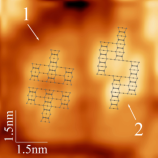
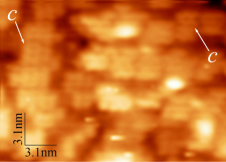
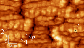
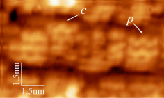
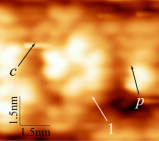
Our approach to the problem is simple. Recently we described two characteristic formations composed by epitaxially oriented Ge dimer pairs and chains of four dimers on the WL patches which were interpreted as two types of hut nuclei: an individual type for each species of huts—pyramids or wedges (Fig. 1).Arapkina and Yuryev (2010a) Being aware of the shapes of the nuclei we can determine by STM a coverage () at which the first generation of nuclei emerge on WL. Then we can trace the evolution of an array and WL until huts with pronounced shapes and faceting form.
II Experimental
Experiments were carried out using a UHV MBE chamber (residual gas pressure Torr) coupled with STM ( Torr).Arapkina and Yuryev (2010b, 2011) Substrates were 88 mm2 squares cut from the specially treated commercial B-doped CZ Si wafers (-type, cm). Ge was deposited on the clean Si(001) surfaceArapkina et al. (2011) from a source with the electron beam evaporation. The deposition rate was Å/s; was varied from 3 to 6 Å for different samples; and were controlled by the Inficon Leybold-Heraeus XTC 751-001-G1 thin film deposition thickness and rate controller with a quartz sensor. The substrate temperature was 360 ℃; the pressure in the MBE chamber did not exceed Torr during Ge deposition. The rate of the sample cooling down to the room temperature was approximately 0.4 ℃/s. After cooling, the samples were moved into the STM chamber. The images were obtained in the constant tunneling current () mode at the room temperature. The STM tip was zero-biased while the sample was positively or negatively biased () for empty or filled states imaging. STM images were processed using the WSxM software.Horcas et al. (2007) A detailed description of the experimental procedures can be found in Ref. Arapkina and Yuryev, 2010b, 2011.
III Data and Discussion
(a)
 (b)
(b)
(a)
 (b)
(b)
 (c)
(c)
 (d)
(d)
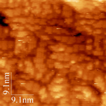
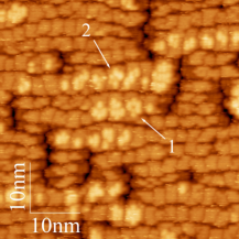
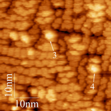
The obtained experimental data are as follows. Fig. 2(a) demonstrates a typical STM micrograph of the ()-patched WL ( Å, ML). This image does not demonstrate any feature which might be recognized as a hut nucleus (Fig. 1).Arapkina and Yuryev (2010a) Such features first arise at the coverages of Å: they are clearly seen in the images (b) to (d), which demonstrate a moment when the array have just nucleated ( Å, ML). However, we succeeded to find minute pyramid and wedge at this (Fig. 2(d))—both as small as 2 ML over the patch surface (we measure cluster heighs from patch tops)—which indicate that hut nucleation had started a little earlier.
It can be concluded from these observations that hut arrays nucleate at a coverage of Å ( ML) when approximately a half of patches are as thick as 4 ML. We can suppose then that huts nucleate on those patches whose thickness reaches (or even exceeds) 4 ML.
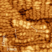
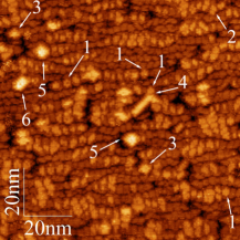
The hut nucleation goes on during further evolution of the array. Fig. 3 illustrates this process. An array shown in Fig. 3(a) ( Å, ML) consists of 1-ML nuclei, 2-ML and 3-ML pyramids and wedges. Fig. 3(b) ( Å, ML) demonstrates the simultaneous presence of nuclei and 2-ML huts with the growing much higher clusters. So, hut arrays initially evolve with increasing by concurrent growth of available clusters and nucleation of new ones resulting in progressive rise of hut number density.
Our data are in very good agreement with the results reported in Ref. Horn-von Hoegen et al., 2004, except for the growth temperature.
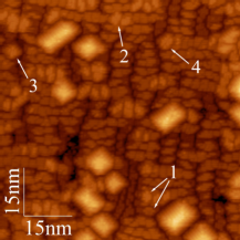
Evolution of WL patches during MBE is illustrated by Fig. 4. In full agreement with the data of Ref. Iwawaki, Tomitori, and Nishikawa, 1992, both and reconstructions are observed on tops of the patches in all images except for the image Fig. 4(a) ( Å) in which only the structure is recognized. Formation of a hut nucleus on a patch reconstructs its surface; a new formation changes the topmost layer structure to that specific for a particular type of nuclei, in the present case, to the structure of the pyramidal hut nucleus (Fig. 4(d)). However the residual structure still remains on the lower terrace of the patch. At the same time, the structure stays on the top of the adjacent patch.
It is necessary to remark here that the nuclei are always observed to arise on sufficiently large WL patches. There must be enough room for a nucleus on a single patch. A nucleus cannot be housed on more than one patch. Thus, cluster nucleation is impossible on little (too narrow or short) patches (Figs. 1 and 4(d)).Arapkina and Yuryev (2010b, a, c)
Note also that both types of nuclei emerge at the same moment of the MBE growth. It means that they are degenerate by the formation energy. Obvious consideration resulting in this conclusion is following: both types of the hut nuclei arise at the same WL thickness (“moment”), hence, at the same WL stress to relief it. So, they appear at the same strain energy (and with equal likelihoods, see Refs. Arapkina and Yuryev, 2010b, a). If they had different formation energies they would appear at different WL thicknesses. The first of the types of huts, which nucleates on the surface, releases the stress. The second one never appears therefore. Hence, they can appear only simultaneously. And their formation energies, as it follows from our observations, can only be equal. Calculations supporting (or refuting) our reasoning are desirable, however, for explanation of why two structures different in symmetry have equal energies and probabilities of formation. Until then, an issue of a reason which makes two different structures arise, rather than one, to relief the WL strain remains open, however.
As of now, we can only propose a very preliminary interpretation of the observed simultaneous appearance of the two kinds of nuclei on WL at the patch thickness of 4 ML. The explanation is based on modeling of Ge cluster formation energy performed in Ref. Brehm et al., 2009. The authors of Ref. Brehm et al., 2009 explore Ge island nucleation during MBE at much higher temperatures than those applied in this work, therefore theoretical results of Ref. Brehm et al., 2009 describe the experimental data obtained for the case of the high-temperature growth mode, which differs considerably from the low-temperature one.Arapkina and Yuryev (2010b) However, the modeling could also apply for the low-temperature growth. The case is that according to Ref. Brehm et al., 2009, flat Ge islands—nuclei and small huts—likely occur on WL because of an energy benefit which arises in exposing the compressed {105} facets, rather than in relaxing the volumetric elastic energy, as it takes place in the usual Stranski-Krastanov mechanism. At low temperatures, this effect may stabilize clusters, however preventing their further ripening (this agrees with our observations presented recently in Ref. Arapkina and Yuryev, 2010b). If this is the case, the actual volumetric form of clusters really does not matter very much in their formation energy, and nucleation probabilities (and energies) of the {105} faceted pyramids or wedges appear to be close in spite of difference in their symmetries.
This model may also be useful for explaining swift elongation of wedges as well as gradual extinction of pyramids during low temperature MBE.Arapkina and Yuryev (2010b) Notice also that the degeneracy of wedge facets is likely removed by a vacancy-type defect which is always present on each triangular facet of a wedge-like hut.Arapkina and Yuryev (2010a, 2011)
IV Conclusion
In summary, the following conclusions are made. At 360 ℃, nuclei of Ge pyramids and wedges are observed on the wetting layer patches starting from the coverage of about Å ( ML). This suggests that huts nucleate on patches of 4 ML thick; the formation energies of both types of nuclei are equal. Further development of hut arrays consists in simultaneous growth of the formerly emerged clusters and nucleation of new ones resulting in gradual rise of hut number density with increasing . Huts nucleate reconstructing the patch surface from the usual or structure to one of two recently described more complicated formations composed by epitaxially oriented Ge dimer pairs and chains of four dimers.
Acknowledgements.
This work was supported by the Ministry of Education and Science of the Russian Federation, the State Contract no. 14.740.11.0069.References
- Mo et al. (1990) Y.-W. Mo, D. E. Savage, B. S. Swartzentruber, and M. G. Lagally, Phys. Rev. Lett. 65, 1020 (1990).
- LeGoues, Copel, and Tromp (1990) F. K. LeGoues, M. Copel, and R. M. Tromp, Phys. Rev. B 42, 11690 (1990).
- Eaglesham and Cerullo (1990) D. J. Eaglesham and M. Cerullo, Phys. Rev. Lett. 64, 1943 (1990).
- Wang et al. (2007) K. L. Wang, D. Cha, J. Liu, and C. Chen, Proc. of the IEEE 95, 1866 (2007).
- Yakimov et al. (2001) A. I. Yakimov, A. V. Dvurechenskii, A. I. Nikiforov, and Y. Y. Proskuryakov, J. Appl. Phys. 89, 5676 (2001).
- Arapkina and Yuryev (2010a) L. V. Arapkina and V. A. Yuryev, Phys. Rev. B 82, 045315 (2010a), arXiv:0907.4665.
- Arapkina and Yuryev (2011) L. V. Arapkina and V. A. Yuryev, Nanoscale Res. Lett. 6, 345 (2011), arXiv:1009.3831.
- Liu, Wu, and Lagally (1997) F. Liu, F. Wu, and M. G. Lagally, Chem. Rev. 97, 1045 (1997).
- Jesson, Kästner, and Voigtländer (2000) D. E. Jesson, M. Kästner, and B. Voigtländer, Phys. Rev. Lett. 84, 330 (2000).
- Arapkina and Yuryev (2010b) L. V. Arapkina and V. A. Yuryev, Phys. Usp. 53, 279 (2010b), arXiv:0907.4770.
- Iwawaki, Tomitori, and Nishikawa (1992) F. Iwawaki, M. Tomitori, and O. Nishikawa, Ultramicroscopy 42–44, 902 (1992).
- Iwawaki, Tomitori, and Nishikawa (1991) F. Iwawaki, M. Tomitori, and O. Nishikawa, Surf. Sci. Lett. 253, L411 (1991).
- Iwawaki et al. (1992) F. Iwawaki, H. Kato, M. Tomitori, and O. Nishikawa, Ultramicroscopy 42–44, 895 (1992).
- Tomitori et al. (1994) M. Tomitori, K. Watanabe, M. Kobayashi, F. Iwawaki, and O. Nishikawa, Surf. Sci. 301, 214 (1994).
- Nikiforov, Cherepanov, and Pchelyakov (2001) A. I. Nikiforov, V. A. Cherepanov, and O. P. Pchelyakov, Semiconductors 35, 998 (2001).
- Dashiell et al. (2002) M. W. Dashiell, U. Denker, C. Müller, G. Costantini, C. Manzano, K. Kern, and O. G. Schmidt, Appl. Phys. Lett. 80, 1279 (2002).
- Horn-von Hoegen et al. (2004) M. Horn-von Hoegen, B. H. Müller, T. Grabosch, and P. Kury, Phys. Rev. B 70, 235313 (2004).
- Lu and Liu (2005) G.-H. Lu and F. Liu, Phys. Rev. Lett. 94, 176103 (2005).
- Arapkina and Yuryev (2010c) L. V. Arapkina and V. A. Yuryev, JETP Lett. 91, 281 (2010c), arXiv:0908.0883.
- Arapkina et al. (2011) L. V. Arapkina, V. A. Yuryev, K. V. Chizh, V. M. Shevlyuga, M. S. Storojevyh, and L. A. Krylova, Nanoscale Res. Lett. 6, 218 (2011), arXiv:1009.3909.
- Horcas et al. (2007) I. Horcas, R. Fernandez, J. M. Gomez-Rodriguez, J. Colchero, J. Gomez-Herrero, and A. M. Baro, Rev. Sci. Instrum. 78, 013705 (2007).
- Brehm et al. (2009) M. Brehm, F. Montalenti, M. Grydlik, G. Vastola, H. Lichtenberger, N. Hrauda, M. J. Beck, T. Fromherz, F. Schäffler, L. Miglio, and G. Bauer, Phys. Rev. B 80, 205321 (2009).