Determination of the bandgap and split-off band of wurtzite GaAs
Abstract
GaAs nanowires with a 100% wurtzite structure are synthesized by the vapor-liquid-solid method in a molecular beam epitaxy system, using gold as a catalyst. We use resonant Raman spectroscopy and photoluminescence to determine the position of the crystal-field split-off band of hexagonal wurtzite GaAs. The temperature dependence of this transition enables us to extract the value at 0 K, which is 1.982 eV. Our photoluminescence excitation spectroscopy measurements are consistent with a band gap of GaAs wurtzite below 1.523 eV.
Nanowires are filamentary crystals with a diameter of the order of few nanometers. Their increasing importance in both science and engineering is a consequence of the great number of novel experiments and applications they enable.Qian et al. (2008, 2004); Xiang et al. (2006); Greytak et al. (2005); Fluegel et al. (2007); Barnham and Duggan (1990); Ferrari et al. (2009) It has been predicted and shown that the reduced diameter of nanowires allows the combination of lattice mismatched materials when they are fabricated in the nanowire form.Glas (2006); Mårtensson et al. (2004) The possibility of obtaining new material combinations opens great perspectives for example in the area of multiple junction photovoltaics.Wallentin et al. (2010) Recently, a new degree of freedom in the formation of heterostructures has appeared. The new type of heterostructure concerns the variation of the crystal phase along the nanowire instead of the material composition.Mattila et al. (2006); Mishra et al. (2007); Birman (1959) The degree of control over the crystal phase can be astonishingly accurate depending on the growth method,Algra et al. (2008); Caroff et al. (2009); Dick et al. (2010) so that perspectives for new device concepts are exciting the nano-science and nanotechnology community.
While the structural control is becoming increasingly sophisticated, few experimental reports have focused on the details of the electronic structure of wurtzite arsenides or phosphides. Recently, two groups applied photoluminescence excitation to determine the valence band structure of wurtzite InP.Perera et al. (2010); Gadret et al. (2010) The results agreed well with the theoretical expectations. Wurtzite GaAs has shown to be more controversial. First, there are significant disagreements between the theoretical calculations of the bandgap.De and Pryor (2010); Murayama and Nakayama (1994) Second, luminescence studies of different groups have shown results consistent with a bandgap of 1.54,Hoang et al. (2009) 1.522,Martelli et al. (2007) and 1.50 eV.Moewe et al. (2008); Spirkoska et al. (2009); Heiss et al. (2011) The apparent lack of agreement between the various groups might be explained by the fact that the optical and structural characterizations were not performed on exactly the same nanowire. Recently, we designed an experiment in which both the luminescence and electron microscopy measurements were realized on the identical nanowire.Heiss et al. (2011) We investigated both nanowires presenting a mixture of wurtzite and zinc-blende and a 100% of wurtzite crystal phase. These and previous experiments were consistent with a bandgap of 1.50 eV for wurtzite GaAs.Spirkoska et al. (2009); Heiss et al. (2011)
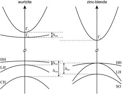
As a consequence of the hexagonal symmetry, it has been shown that the band structure of wurtzite semiconductors exhibits important differences compared to the band structure of the respective zinc-blende (cubic) counterparts.De and Pryor (2010) In Fig. 1 we compare the band structure of zinc-blende and wurtzite GaAs close to the point according to recent theoretical results from De and Pryor.De and Pryor (2010) As a consequence of the zone folding induced by the doubling of the unit cell along the (111) direction an additional conduction band with symmetry appears for the wurtzite structure. In contrast to other III-V semiconductors the energy separation between these two conduction bands is expected to be the smallest for the case of wurtzite GaAs. The theoretical predicted values of meV,Murayama and Nakayama (1994) meV,De and Pryor (2010) or meVHeiss et al. (2011) are even smaller than the predicted splitting of the two uppermost valence bands. There, the crystal field splitting and spin-orbit interaction lift the degeneracy of the heavy and light hole states for the wurtzite structure.De and Pryor (2010); Chuang and Chang (1996) Furthermore a crystal-split-off hole (CH) band is predicted further down in energy below the valence band edge compared to the split-off band in zinc-blende GaAs.De and Pryor (2010) To the best of our knowledge, there are to date no studies providing the values of either the crystal splitting or split-off band for the case of wurtzite GaAs.
Luminescence studies allow the probing of transitions between the conduction band minimum and the highest energy valence band states. In order to obtain information on the valence band structure, i.e. crystal and split-off band splitting, other type of experiments such as photoluminescence excitation and resonant Raman scattering should be implemented.Perera et al. (2010); Pistol et al. (1992); Sköld et al. (2009); Calleja and Cardona (1977) In this paper we use resonant Raman scattering and photoluminescence excitation spectroscopy to probe the crystal-field (CH) split-off valence band to conduction band transition and to provide more clarity and consistence in recent luminescence studies that attributed the bandgap of wurtzite to be at 1.50 eV.
Wurtzite GaAs nanowires were grown by the Au-catalyzed Vapor-liquid-solid method on GaAs ()B substrates at a growth temperature of 540 ∘C under a As4 Beam flux of Torr at a Ga rate equivalent to a planar growth of 0.4 Å/s. The growth time was 4 hours. The nucleation and growth followed the Vapor-Liquid-Solid mechanism, with Au as catalyst.Wagner and Ellis (1964) Details on the growth procedure are described in.Rudolph et al. (2009) After the axial growth of the nanowires the growth parameters were changed to conditions suitable for planar growth and the nanowires were passivated by an epitaxial prismatic shell of AlGaAs/GaAs material.Fontcuberta i Morral et al. (2008) The 2D equivalent amount grown during capping was 60 nm AlGaAs followed by 30 nm GaAs. The total diameter of the nanowires is approximately 85 nm. The structure has shown to be 100% wurtzite with a few twin planes.Heiss et al. (2011)
Single nanowire spectroscopy was realized on nanowires dispersed on a marked silicon substrate. In the Raman spectroscopy experiments, the nanowires were photoexcited by Ar+Kr+ or HeNe lasers with wavelengths respectively 647.1 nm and 632.8 nm. In the photoluminescence excitation spectroscopy measurements (PLE), the excitation source was a Koheras SuperK super continuum source filtered by an acusto-optical tunable filter (AOTF). During the PLE measurement the actual power of the excitation light was kept constant throughout the entire wavelength range by means of a computer controlled feedback loop. Both in the Raman and PLE spectroscopy experiments, the light was focused to a sub-micron spot using a cover glass corrected 0.75 NA microscope objective. The measurements were realized at a temperature between 10 and 360 K in a liquid helium flow cryostat. The scattered light was collected through the same objective and focused on the entrance slit of a triple spectrometer and the spectrum collected thanks to a peltier cooled charge coupled device.
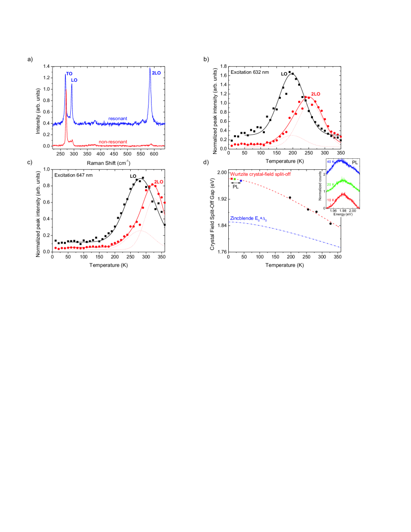
We first present the resonant Raman scattering experiment. Here, we look for the conditions leading to sharp resonances of the first and second order LO phonons that occur via the dipole-forbidden Fröhlich electron-phonon interaction.Trommer and Cardona (1978); Kauschke et al. (1987) The resonance is observed when the excitation energy coincides with an interband critical point in the joint density of states of the semiconductor. In our case, we reach the transition between the split-off valence and the conduction band. Typical Raman spectra of wurtzite GaAs obtained in polarized configuration with the incident and detected polarization parallel to the c-axis, which lies along the nanowire axis, are shown in Fig. 2a. This configuration is denoted as in Porto notation. We plot the spectra under non-resonant and resonant conditions, the difference being the intensity of the LO and 2LO peaks. Under non-resonant conditions, only the (TO) mode at 270 cm-1 is allowed in configuration.Zardo et al. (2009); Crankshaw et al. (2010) Under resonant conditions, not only the intensity of the dipole-forbidden (LO) mode at 290 cm-1 increases significantly but also the second order Raman scattering by two (LO) phonons at 580 cm-1 is strongly enhanced.Brewster et al. (2009) For simplicity, in the following we will denominate the (TO) and (LO) modes as simply TO and LO.
Now we proceed with the determination of the resonance Raman conditions for the measurement of the critical points of wurtzite GaAs. We measured the Raman spectra of single wurtzite GaAs nanowires as a function of the excitation energy and temperature. The excitation wavelengths used were 632.8 and 647.1 nm. The temperature was varied between 10 and 360 K. The intensity of the LO and 2LO peaks normalized to the intensity of the TO mode as a function of temperature for the excitation at 632.8 and 647.1 nm are shown respectively in Fig. 2b and c. The resonance profile of the LO phonon scattering shows a single maximum under outgoing resonance, where the scattered light exactly matches a gap of the electronic band structure. The 2LO phonon scattering reveals a strong outgoing resonance () as well as a weaker intermediate resonance (). No incoming resonance is observed neither for the LO nor the 2LO scattering. For the excitation at 632.8 nm, we observe the strongest resonance of the LO and 2LO peaks respectively at 197 and 255 K. For the excitation at 647.1 nm, we observe it at 282 and 327 K. For these temperatures, the energy of the critical point is then calculated:
| (1) |
where corresponds to the frequency of the phonons (LO or 2LO) and is the excitation wavelength. For the temperatures of 197, 255, 282, and 327 K, under which the resonances occur, we obtain respectively critical energies of 1.925, 1.889, 1.882, and 1.846 eV. These points are reported in Fig. 2d. Limitations in wavelengths we have available do not allow us to obtain the energy of this transition at lower temperatures. Nevertheless, we have tried to measure direct luminescence from the recombination between the two resonant levels. Due to the very few non occupied states in the CH split-off band, such a transition is extremely weak. We have obtained luminescence of this transition for an incident polarization parallel to the hexagonal c-axis at temperatures between 10 and 40 K by exciting with 568.2 nm and a power of 50 W. The acquisition time was 30 min, which is between three and four orders of magnitude longer than our typical luminescence experiments in our nanowires for equivalent excitation powers. The spectra are shown in the inset of Fig. 2d. At temperatures of 10, 20 and 40 K we observe respectively PL centered at 1.982, 1.981, and 1.976 eV. This enables us to complete the curve of the temperature dependence. The temperature dependent variation of the band gap energy can be commonly given in terms of the and coefficients of the Varshni equation:Varshni (1967)
| (2) |
Least-squares fitting to the experimental data, the result is shown in Fig. 2d, gives the fitting parameters and as eV/K and 245.8 K, respectively. For K we find a gap energy of eV. We now discuss the nature of the extrapolated interband critical point eV in wurtzite GaAs. In zinc-blende GaAs, the interband transition from the spin-orbit-split valence band to the lowest conduction band at the point is found at 1.851 eVLautenschlager et al. (1987) for K (see Fig. 2d). Likewise, we attribute the observed energy gap in wurtzite GaAs to a transition from the crystal-field split-off valence band to one of the lowest energy conduction bands at the point of the Brillouin zone. For the discussion, we need to come back to Fig. 1. The crystal-field split-off valence band is labeled with CH. This band has a symmetry. In the conduction band there is an important difference with respect to zinc-blende. There is one first minimum labeled , which originates from the zone-folded L-valleys of zinc-blende GaAs. This band is separated by a small energy fraction from a close lying conduction band with symmetry. According to the selection rules in materials with hexagonal wurtzite structure, optical transitions from the CH valence band to the conduction band are dipole allowed. Transitions from the valence band to the conduction band are dipole forbidden.Tronc et al. (1999) Generally, these selection rules may be softened in resonant Raman exciting conditions,Martin and Falicov (1983) meaning that resonant Raman scattering from an optically forbidden transition cannot be completely excluded. However, the fact that we observe photoluminescence from this energy gap let us conclude that the transition should be the dipole allowed CH () to . Consequently, we assign the observed critical point with energy of 1.982 eV in wurtzite GaAs to the interband transition from the crystal-field split-off valence band to the second lowest conduction band. Finally, we compare the experimental findings with theoretical predictions. Based on an empirical pseudopotential method including spin-orbit coupling, De und Pryor calculated values of respectively 1.978 eV and 2.063eV for the to and to interband transitions. This means that our experiment agrees within 4% (81 meV) with this theory.
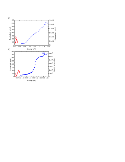
For a further understanding of the band structure of wurtzite GaAs, photoluminescence excitation spectroscopy was realized. A typical PL spectrum of a single nanowire is shown in Fig. 3a. A single peak centered at 1.515 eV is observed, consistent with our previous works.Heiss et al. (2011) The excitation spectroscopy measurements were realized by detecting the integrated intensity of the emission as a function the excitation energy. The resulting PLE measurements on single nanowires are shown in Fig. 3a. We start by describing the measurements realized at high photon energies of the excitation light, between 1.58 and 1.85 eV, shown in Fig. 3a. The power density for these measurements was in the order of 300 W/cm2. We observe a relatively sharp increase in the signal at 1.6 eV. We believe the increased signal comes from a contribution of the Al0.33Ga0.67As shell, which exhibits about 2.7 times the volume of the nanowire core in the present sample. The electron-hole pairs generated in the shell can diffuse and recombine the wurtzite GaAs core, thereby contributing to the PLE signal. The bandgap of wurtzite-AlAs is theoretically expected to be significantly smaller compared to the (indirect band-gap) zinc-blende counterpart as a result of the zone-folding along the direction.De and Pryor (2010); Murayama and Nakayama (1994) A recombination around 1.6 eV is consistent with recent measurements on wurtzite AlxGa1-xAs with comparable nominal composition.Zhou et al. (2009) In principle this transition could also be in reasonable agreement with a transition from the heavy-hole band to the second conduction band with symmetry that is predicted at 1.588 eV, and even with a transition from the light-hole band to the conduction band (1.623 eV).De and Pryor (2010) However, according to theory, the transition to should not be dipole allowedTronc et al. (1999) and furthermore the transitions related to the light-hole band or the conduction band should be weak due to the smaller joint density of states.De and Pryor (2010) We therefore believe that the increase in PLE signal around 1.6 eV signal is predominantly caused by the onset of absorption in the wurtzite Al0.33Ga0.67As shell.
Finally, we turn our attention to PLE measurements realized closer to the bandgap. In order to approach the band gap with the excitation source the spectral output of the AOTF had to be further narrowed by passing the excitation light through a monochromator (f=300 mm, Grating: 150 Grooves/mm) and subsequently projecting the light from the exit slit of this monochromator to the sample. This enabled us to narrow down the linewidth below 1 nm and to remove the remaining background emission from the AOTF. This further step also limited the maximum excitation power density down to about 10 W/cm2. As a consequence, the collected signal was significantly reduced with respect to the measurements for excitation energies higher than 1.6 eV. In order to increase the signal to noise ratio for the energy range between 1.525 and 1.68 eV, we realized measurements on nanowire ensembles. As shown in Fig. 3b, the PL spectrum of the ensemble is extremely similar to that of single nanowires. This is possible because all nanowires present the identical structure. Consistent with the measurements at higher excitation energies, we observe an increase in PLE intensity around 1.6 eV. For energies below 1.6 eV and down to 1.523 eV, no other clearly resolvable PLE feature is observed. One should note that the PL spectrum shown in Fig. 3b corresponds to the one obtained at the excitation energy of 1.527 eV. We therefore estimate the Stokes shift - the energy offset between the emission peak and the onset of absorption - to be smaller than 10 meV. From our PLE measurements we can estimate an upper limit for the band gap of wurtzite GaAs to 1.523 eV. As we have discussed in detail previously,Heiss et al. (2011) taking into account quantum confinement effects, the emission peak is in reasonable agreement with predictions of De and Pryor of a bulk wurtzite band-gap of 1.503 eV.De and Pryor (2010) At the same time, our PLE data are inconsistent with a band-gap of 1.552 eV as predicted by Murayama and Nakayama,Murayama and Nakayama (1994) as no feature is observed in the corresponding spectral region.
In conclusion, we have measured the position of the crystal-field split-off band of wurtzite GaAs by resonant Raman and photoluminescence spectroscopy. The temperature dependence was fit with the Varshni equation and the parameters were extracted. A value of 1.982 eV was obtained for the CH split-off to conduction band transition at 0 K. PLE measurements down to 1.525 eV are consistent with a bandgap of wurtzite GaAs below 1.523 eV and inconsistent with a transition at 1.55 eV.
Acknowledgements.
The authors thank A. Rudolph and D. Schuh for their experimental support. We thank financial support of by the Swiss National Science Foundation under Grant No. 2000021-121758/1 and 129775/1 by the European Research Council under Grant ‘Upcon’.References
- Qian et al. (2008) F. Qian, Y. Li, S. Gradečak, H.-G. Park, Y. Dong, Y. Ding, Z. L. Wang, and C. M. Lieber, Nat Mater 7, 701 (2008).
- Qian et al. (2004) F. Qian, Y. Li, S. Gradečak, D. Wang, C. J. Barrelet, and C. M. Lieber, Nano Letters 4, 1975 (2004).
- Xiang et al. (2006) J. Xiang, W. Lu, Y. Hu, Y. Wu, H. Yan, and C. M. Lieber, Nature 441, 489 (2006).
- Greytak et al. (2005) A. B. Greytak, C. J. Barrelet, Y. Li, and C. M. Lieber, Applied Physics Letters 87, 151103 (2005).
- Fluegel et al. (2007) B. Fluegel, A. Mascarenhas, D. W. Snoke, and K. Pfeiffer, L. N.and West, Nat Photon 1, 701 (2007).
- Barnham and Duggan (1990) K. W. J. Barnham and G. Duggan, Journal of Applied Physics 67, 3490 (1990).
- Ferrari et al. (2009) G. Ferrari, G. Goldoni, A. Bertoni, G. Cuoghi, and E. Molinari, Nano Letters 9, 1631 (2009).
- Glas (2006) F. Glas, Phys. Rev. B 74, 121302 (2006).
- Mårtensson et al. (2004) T. Mårtensson, C. P. T. Svensson, B. A. Wacaser, M. W. Larsson, W. Seifert, K. Deppert, A. Gustafsson, L. R. Wallenberg, and L. Samuelson, Nano Letters 4, 1987 (2004).
- Wallentin et al. (2010) J. Wallentin, J. M. Persson, J. B. Wagner, L. Samuelson, K. Deppert, and M. T. Borgström, Nano Letters 10, 974 (2010).
- Mattila et al. (2006) M. Mattila, T. Hakkarainen, M. Mulot, and H. Lipsanen, Nanotechnology 17, 1580 (2006).
- Mishra et al. (2007) A. Mishra, L. V. Titova, T. B. Hoang, H. E. Jackson, L. M. Smith, J. M. Yarrison-Rice, Y. Kim, H. J. Joyce, Q. Gao, H. H. Tan, and C. Jagadish, Applied Physics Letters 91, 263104 (2007).
- Birman (1959) J. L. Birman, Phys. Rev. Lett. 2, 157 (1959).
- Algra et al. (2008) R. E. Algra, M. A. Verheijen, M. T. Borgstrom, L.-F. Feiner, G. Immink, W. J. P. van Enckevort, E. Vlieg, and E. P. A. M. Bakkers, Nature 456, 369 (2008).
- Caroff et al. (2009) P. Caroff, K. A. Dick, J. Johansson, M. E. Messing, K. Deppert, and L. Samuelson, Nat Nano 4, 50 (2009).
- Dick et al. (2010) K. A. Dick, C. Thelander, L. Samuelson, and P. Caroff, Nano Letters 10, 3494 (2010).
- Perera et al. (2010) S. Perera, K. Pemasiri, M. A. Fickenscher, H. E. Jackson, L. M. Smith, J. Yarrison-Rice, S. Paiman, Q. Gao, H. H. Tan, and C. Jagadish, Applied Physics Letters 97, 023106 (2010).
- Gadret et al. (2010) E. G. Gadret, G. O. Dias, L. C. O. Dacal, M. M. de Lima, C. V. R. S. Ruffo, F. Iikawa, M. J. S. P. Brasil, T. Chiaramonte, M. A. Cotta, L. H. G. Tizei, D. Ugarte, and A. Cantarero, Phys. Rev. B 82, 125327 (2010).
- De and Pryor (2010) A. De and C. E. Pryor, Phys. Rev. B 81, 155210 (2010).
- Murayama and Nakayama (1994) M. Murayama and T. Nakayama, Phys. Rev. B 49, 4710 (1994).
- Hoang et al. (2009) T. B. Hoang, A. F. Moses, H. L. Zhou, D. L. Dheeraj, B. O. Fimland, and H. Weman, Applied Physics Letters 94, 133105 (2009).
- Martelli et al. (2007) F. Martelli, M. Piccin, G. Bais, F. Jabeen, S. Ambrosini, S. Rubini, and A. Franciosi, Nanotechnology 18, 125603 (2007).
- Moewe et al. (2008) M. Moewe, L. C. Chuang, S. Crankshaw, C. Chase, and C. Chang-Hasnain, Applied Physics Letters 93, 023116 (2008).
- Spirkoska et al. (2009) D. Spirkoska, J. Arbiol, A. Gustafsson, S. Conesa-Boj, F. Glas, I. Zardo, M. Heigoldt, M. H. Gass, A. L. Bleloch, S. Estrade, M. Kaniber, J. Rossler, F. Peiro, J. R. Morante, G. Abstreiter, L. Samuelson, and A. Fontcuberta i Morral, Phys. Rev. B 80, 245325 (2009).
- Heiss et al. (2011) M. Heiss, S. Conesa-Boj, J. Ren, H.-H. Tseng, A. Gali, A. Rudolph, E. Uccelli, F. Peiró, J. R. Morante, D. Schuh, E. Reiger, E. Kaxiras, J. Arbiol, and A. Fontcuberta i Morral, Phys. Rev. B 83, 045303 (2011).
- Chuang and Chang (1996) S. L. Chuang and C. S. Chang, Phys. Rev. B 54, 2491 (1996).
- Pistol et al. (1992) M.-E. Pistol, M. Gerling, D. Hessman, and L. Samuelson, Phys. Rev. B 45, 3628 (1992).
- Sköld et al. (2009) N. Sköld, M.-E. Pistol, K. A. Dick, C. Pryor, J. B. Wagner, L. S. Karlsson, and L. Samuelson, Phys. Rev. B 80, 041312 (2009).
- Calleja and Cardona (1977) J. M. Calleja and M. Cardona, Phys. Rev. B 16, 3753 (1977).
- Wagner and Ellis (1964) R. S. Wagner and W. C. Ellis, Applied Physics Letters 4, 89 (1964).
- Rudolph et al. (2009) A. Rudolph, M. Soda, M. Kiessling, T. Wojtowicz, D. Schuh, W. Wegscheider, J. Zweck, C. Back, and E. Reiger, Nano Letters 9, 3860 (2009).
- Fontcuberta i Morral et al. (2008) A. Fontcuberta i Morral, D. Spirkoska, J. Arbiol, M. Heigoldt, J. R. Morante, and G. Abstreiter, Small 4, 899 (2008).
- Lautenschlager et al. (1987) P. Lautenschlager, M. Garriga, S. Logothetidis, and M. Cardona, Phys. Rev. B 35, 9174 (1987).
- Trommer and Cardona (1978) R. Trommer and M. Cardona, Phys. Rev. B 17, 1865 (1978).
- Kauschke et al. (1987) W. Kauschke, M. Cardona, and E. Bauser, Phys. Rev. B 35, 8030 (1987).
- Zardo et al. (2009) I. Zardo, S. Conesa-Boj, F. Peiro, J. R. Morante, J. Arbiol, E. Uccelli, G. Abstreiter, and A. Fontcuberta i Morral, Phys. Rev. B 80, 245324 (2009).
- Crankshaw et al. (2010) S. Crankshaw, L. C. Chuang, M. Moewe, and C. Chang-Hasnain, Phys. Rev. B 81, 233303 (2010).
- Brewster et al. (2009) M. Brewster, O. Schimek, S. Reich, and S. Gradečak, Phys. Rev. B 80, 201314 (2009).
- Varshni (1967) Y. P. Varshni, Physica 34, 149 (1967).
- Tronc et al. (1999) P. Tronc, Y. Kitaev, G. Wang, M. Limonov, A. Panfilov, and G. Neu, phys. stat. sol. (b) 216, 599 (1999).
- Martin and Falicov (1983) R. Martin and L. Falicov, in Light Scattering in Solids I, Topics in Applied Physics, Vol. 8 (Springer Berlin / Heidelberg, 1983) pp. 79–145.
- Zhou et al. (2009) H. L. Zhou, T. B. Hoang, D. L. Dheeraj, A. T. J. van Helvoort, L. Liu, J. C. Harmand, B. O. Fimland, and H. Weman, Nanotechnology 20, 415701 (2009).