STM Spectroscopy of ultra-flat graphene on hexagonal boron nitride
Abstract
Graphene has demonstrated great promise for future electronics technology as well as fundamental physics applications because of its linear energy-momentum dispersion relations which cross at the Dirac pointGeim2007 ; CastroNeto2009 . However, accessing the physics of the low density region at the Dirac point has been difficult because of the presence of disorder which leaves the graphene with local microscopic electron and hole puddlesMartin2008 ; Deshpande2009 ; Zhang2009 , resulting in a finite density of carriers even at the charge neutrality point. Efforts have been made to reduce the disorder by suspending graphene, leading to fabrication challenges and delicate devices which make local spectroscopic measurements difficultDu2008 ; Bolotin2008 . Recently, it has been shown that placing graphene on hexagonal boron nitride (hBN) yields improved device performanceDean2010 . In this letter, we use scanning tunneling microscopy to show that graphene conforms to hBN, as evidenced by the presence of Moiré patterns in the topographic images. However, contrary to recent predictionsGiovannetti2007 ; Slawinska2010 , this conformation does not lead to a sizable band gap due to the misalignment of the lattices. Moreover, local spectroscopy measurements demonstrate that the electron-hole charge fluctuations are reduced by two orders of magnitude as compared to those on silicon oxide. This leads to charge fluctuations which are as small as in suspended grapheneDu2008 , opening up Dirac point physics to more diverse experiments than are possible on freestanding devices.
Graphene was first isolated on silicon dioxide because of the ability to image monolayer regions using an optical microscopeNovoselov2005 . However, the electronic properties of SiO2 are not ideal for graphene because of its high roughness and trapped charges in the oxide. These impurity-induced charge traps tend to cause the graphene to electronically break up into electron and hole doped regions at low charge density which both limit device performance and make the Dirac point physics inaccessibleMartin2008 ; Deshpande2009 ; Zhang2009 ; Chen2008 ; Rossi2008 . In order to create devices with less puddles, the substrate must be removed or changed. One possibility to get rid of substrate interactions is to suspend grapheneDu2008 ; Bolotin2008 , as shown by the drastic improvement in mobility which has enabled the observation of the fractional quantum Hall effect in suspended devicesDu2009 ; Bolotin2009 . However, the freely suspended monolayers are very delicate, leading to fabrication difficulties as well as strainBao2009 . Because of these difficulties, there have been no STM spectroscopy measurements of the local electronic properties of suspended graphene devices. All of this points to the need for new substrates that offer mechanical support to the graphene without interfering with its electrical properties. Recently, such a candidate substrate has been found with the demonstration of high-quality graphene devices on hexagonal boron nitride (hBN)Dean2010 . Hexagonal boron nitride has the same atomic structure as graphene, but with a 1.8% longer lattice constantLiu2003 , and shares many similar properties with graphene except that it is a wide-bandgap electric insulatorWatanabe2004 . The planar structure of hBN cleaves into an ultra-flat surface and the ionic bonding of hBN should leave it free of dangling bonds and charge traps at the surface resulting in less induced electron-hole puddles in graphene. Indeed, graphene on hBN devices exhibit the highest mobility reported on any substrate, as well as narrow Dirac peak resistance widths, indicating reduced disorder and charge inhomogeneityDean2010 .
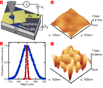
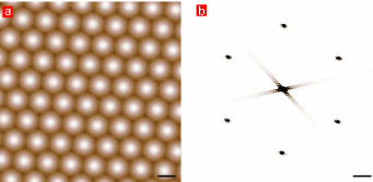
To study how the local electronic structure of graphene is affected by the hBN substrate, we prepare graphene on hBN devices for STM measurements. A schematic of the measurement set-up showing the graphene flake on hBN with gold electrodes for electrical contact is shown in Fig. 1a. A typical STM image of the monolayer graphene showing the surface corrugations due to the underlying hBN substrate is shown in Fig. 1b. This image can be compared with an STM image of monolayer graphene prepared in a similar manner but on SiO2 as shown in Fig. 1c. It is clear from these two images that the surface corrugations are much larger for graphene on SiO2 as compared to hBN. This is due to the graphene conforming to the substrate and the planar nature of hBN as compared to the amorphous SiO2. Figure 1d shows a histogram of the heights in the two images. In both cases, the heights are well described by gaussian distributions with standard deviations of 224.5 0.9 pm for graphene on SiO2 and 30.2 0.2 pm for graphene on hBN. The values for graphene on SiO2 are similar to previously reported values Ishigami2007 ; Stolyarova2007 while the distribution for graphene on hBN is similar to graphene on mica or HOPGLui2009 . Reducing the surface roughness is critical for graphene devices because local curvature can lead to electronic effects such as dopingKim2009 and random effective magnetic fieldsGuinea2008 . As the height variation of the graphene on hBN is as flat as HOPG, it has reached its ultimate limit of flatness.
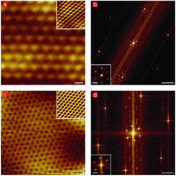
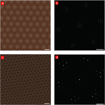
Looking more closely at the topography of the graphene on hBN, we resolve its atomic lattice and also observe longer periodic modulations which result in a distinct Moiré pattern as seen in Figs. 2a and 2c. These two images were acquired from different areas of the same graphene flake and show Moiré patterns of different length due to a shift in the alignment of the graphene with the underlying hBN lattice. In the case of Figs. 2a and 2c, we find a long wavelength modulation of 2.6 nm and 1.3 nm respectively. By examining the Fourier transform of these images, we can learn about the underlying hBN substrate as well as its relative orientation with respect to the graphene lattice. In both cases, we see two distinct sets of peaks in the FFT, there is a set of six points near the center of the images which correspond to the Moiré pattern and there are six additional points near the edge of the images which correspond to the graphene atomic lattice. The first observation is that the locations of these points is rotated with respect to each other in the two images. For Fig. 2b, the atomic lattice is rotated by 12.6 1.0∘ from the horizontal. In the case of Fig. 2d, the atomic lattice is rotated by 18.5 0.6∘. In contrast the Moiré pattern is rotated by 29.9 0.1∘ from the horizontal in Fig. 2b and 38.4 0.2∘ from the horizontal in Fig. 2d. From the lengths of the Moiré patterns and their angles, we can calculate the orientation of the graphene lattice with respect to the underlying hBN (see Supplementary Information). In the case of Fig. 2a, we find that the hBN is rotated by -5.4∘ from the graphene. On the other hand, for Fig. 2c, we find that the hBN is rotated by -10.9∘. This difference of 5.5∘ matches the difference in the orientation of the graphene lattices in the two images. Therefore, we conclude that the underlying hBN substrate is continuous and the graphene above it sits at two different angles. Atomic force microscopy images show that graphene on hBN tends to form flat regions separated by ridges and pyramids. As the two STM images were taken from different sides of one of these ridges, it is clear that the graphene can change orientation across these ridges.
The scanning tunneling microscope is not only able to acquire images of atoms but can also map the local density of states. We have performed scanning tunneling spectroscopy of the graphene on hBN. Figure 3a shows a typical dI/dV spectroscopy curve which is proportional to the local density of states. The curve is nearly linear in energy with a minimum near zero tip voltage indicating the energy of the Dirac point. The location of this minimum can be varied by applying a back gate voltage, , to the sample. The voltage on the back gate induces a charge on the graphene of with e/cm2V based on a parallel plate capacitor model. In the model, we have taken 285 nm of SiO2 with a dielectric constant of 3.9 and 14 nm of hBN with a dielectric constant of 3-4Young2010 . There is a small uncertainty in the value of of about 1% due to the unknown precise value of the hBN dielectric constant. Figure 3b plots dI/dV as a function of tip voltage and gate voltage. The white line follows the minimum in the dI/dV curves for each value of the gate voltage. This minimum occurs when the Fermi energy of the tip lines up with the Dirac point. We observe that the location of the minimum changes more quickly when the Dirac point is near zero tip voltage which is consistent with the linear band structure of graphene. There is also a dark ridge that occurs at decreasing tip voltage as the gate voltage is increased. This is due to the effect of the voltage on the tip acting as a local gate and changing the density of electrons in the grapheneChoudhury2010 .
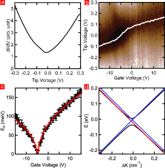
Our local spectroscopy measurements indicate that there is no band gap induced in graphene on hBN, not even locally. These results disagree with earlier theoretical calculations which predicted the opening of a band gap of order 50 meV when graphene is placed on hBN, because of the breaking of sublattice symmetryGiovannetti2007 ; Slawinska2010 . This discrepancy is explained by the 1.8% mismatch between the graphene and hBN lattices and the different orientations of the two lattices, which were both neglected in Refs. Giovannetti2007 ; Slawinska2010 . Taking them into account, one expects that, while one of the carbon atoms may sit over a boron (nitrogen) atom at one location, this alignment gets lost a few lattice constants away. In large enough systems, carbon atoms should therefore have the same probability to have a boron or a nitrogen atom as nearest neighbor in the hBN layer, regardless of their sublattice index. We numerically checked the validity of this hypothesis by calculating the interlayer hopping potential from a carbon atom at in the graphene layer to a boron or nitrogen atom at in a rotated hBN layer. We restricted ourselves to nearest- and next-nearest-neighbor interlayer hopping and chose the parameters eV and nm to fit known values for these hoppings in graphene bilayersZhang2008 . We found that the 1.8% lattice mismatch alone is sufficient to make the hopping strength from a carbon atom to a boron or a nitrogen atom independent of the graphene sublattice index for systems of a few hundred unit cells, going down to a few tens of unit cells when the lattices are misaligned by about one degree. We incorporated the Fourier transform of this hopping potential into the low-energy Hamiltonian for graphene on hBN to find the energy-momentum dispersion. The inter-layer coupling is nonzero only for as well as for six additional vectors associated with the Moiré pattern. Most importantly, we found that the coupling between the A and B atoms in the graphene lattice with the boron and nitrogen atoms in the hBN are almost identical. Thus sublattice symmetry is restored and a gapless Dirac spectrum is recovered, albeit at slightly shifted values of . This is illustrated in Fig. 3d. While depends in principle on whether hopping occurs between a carbon and a boron or nitrogen atom, we note that this does not break sublattice symmetry, and we checked that the spectrum remains gapless, even when this discrepancy is taken into account. More details of our numerical approach are given in the Supplementary Information.
By determining the energy of the Dirac point as a function of gate voltage, we can measure the Fermi velocity of electrons and holes in graphene. Figure 3c shows the energy of the Dirac point as a function of gate voltage. Graphene has a linear dispersion relation such that where is the Fermi velocity. Since it is a two-dimensional material, the density of electrons is given by where and are the spin and valley degeneracy which are both 2 for graphene. Therefore, the Dirac point should depend on gate voltage as . The red curve is a fit to the data from which we can extract the Fermi velocity. We find that m/s for the electrons and m/s for the holes. Moreover, we observe an asymmetry between the Fermi velocity for electrons and holes of about 25% depending on the Moiré pattern observed. The shorter Moiré pattern has a higher Fermi velocity for holes while the longer one has a higher Fermi velocity for electrons. The origin of this asymmetry is unclear but may arise due to next-nearest neighbor coupling which are not taken into account in our model.
One of the main advantages to using hBN as a substrate for graphene as compared to SiO2 is the improvement in electronic properties of the graphene which is believed to be due to the lack of charge traps on the hBN surface. Figure 4a shows the topography of graphene on hBN over a range of 100 nm. Note that the height variation is less than 0.1 nm over the range of the image as compared to typical values of nearly 1 nm for graphene on SiO2. We have performed dI/dV measurements at 1 nm intervals over the entire area of Fig. 4a. For each of these dI/dV curves, we have found tip voltage of the minimum which corresponds to the Dirac point. The results are plotted in Fig. 4b. We have done a similar analysis for a 100 nm area of graphene on SiO2 and the results are plotted in Fig. 4c. The red and blue regions correspond to electron and hole puddles respectively. It is clear from these two images that the variation in the energy of the Dirac point is much smaller on hBN. The spatial extent of each puddle is also much smaller in the graphene on SiO2 consistent with an increased density of impuritiesRossi2008 .
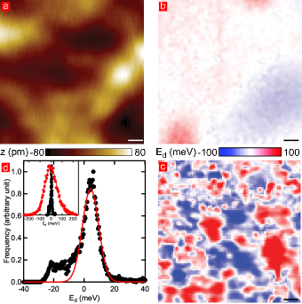
We can further quantify the disorder in the graphene by looking at a histogram of the energy of the Dirac point, Fig. 4d. The main part of the histogram for the Dirac point energy on hBN is well fit by a gaussian distribution (red line) with a standard deviation of meV. In addition, there is a small extra bump in the distribution from the hole doped region near the bottom right of Fig. 4b. In comparison, the distribution on SiO2 is much broader with a standard deviation of meV. These distributions in energy can be converted to charge fluctuations using . We find that the charge fluctuations in graphene on hBN are cm-2 while they are more than 100 times larger for graphene on SiO2, cm-2. Our measurements for the charge fluctuations on SiO2 are consistent with previous single electron transistorMartin2008 and STMDeshpande2009 ; Zhang2009 measurements which established the presence of electron and hole puddles in graphene on SiO2. Furthermore, our measurements for the charge fluctuations in graphene on hBN show a very similar value to values extracted from electrical transport measurements in suspended graphene samplesDu2008 implying that using hBN as a substrate provides a similar benefit to suspending graphene without the associated fabrication challenges and limitations.
We have demonstrated that graphene on hBN provides an extremely flat surface that has significantly reduced electron-hole puddles as compared to SiO2. By reducing the charge fluctuations, the low density regime and the Dirac point can be more readily accessed. Moreover, hBN allows this low-density regime to be reached in a substrate-supported system which will allow atomic resolution local probes studies of the Dirac point physics.
Methods
Thin and flat few layer hBN flakes were prepared by mechanical exfoliation of hBN single crystals on SiO2/Si substrates. The hBN growth method has been previously describedTaniguchi2007 . Exfoliated graphene flakes were then transferred to the hBN using Poly(methyl methacrylate) (PMMA) as a carrier Dean2010 . Then Cr/Au electrodes were deposited using standard electron beam lithography. The lithography process leaves some PMMA resist on the surface of graphene which is cleaned by annealing in argon and hydrogen at 350∘ C for 3 hours meyer2007 . The device was then immediately transferred to the STM (Omicron low temperature STM operating at T = 4.5 K in ultrahigh vacuum (p mbar)). Electrochemically etched tungsten tips were used for imaging and spectroscopy. All of the tips used were first checked on an Au surface to ensure that their density of states was constant.
The dI/dV spectroscopy was acquired by turning off the feedback loop and holding the tip a fixed distance above the surface. A small ac modulation of 5 mV at 563 Hz was applied to the tip voltage and the corresponding change in current was measured using lock-in detection. We also measured dI/dV curves with 0.5 mV excitation and observed the same results.
References
- (1) Geim, A. K. and Novoselov, K. S. The rise of graphene. Nature Mater. 6, 183-191 (2007).
- (2) Castro Neto, A. H., Guinea, F., Peres, N. M. R., Novoselov, K. S., and Geim, A. K. The electronic properties of graphene. Rev. Mod. Phys. 81, 109-162 (2009).
- (3) Martin, J. et al. Observation of electron-hole puddles in graphene using a scanning single-electron transistor. Nature Phys. 4, 144-148 (2008).
- (4) Deshpande, A., Bao, W., Miao, F., Lau, C. N., and LeRoy, B. J. Spatially resolved spectroscopy of monolayer graphene on SiO2. Phys. Rev. B 79, 205411 (2009).
- (5) Zhang, Y., Brar, V. W., Girit, C., Zettl, A., and Crommie, M. F. Origin of spatial charge inhomogeneity in graphene. Nature Phys. 5, 722-726 (2009).
- (6) Du, X., Skachko, I., Barker, A., and Andrei, E. Y. Approaching ballistic transport in suspended graphene. Nature Nanotech. 3, 491-495 (2008).
- (7) Bolotin, K. I., Sikes, K. J., Hone, J., Stormer, H. L., and Kim, P. Temperature-dependent transport in suspended graphene. Phys. Rev. Lett. 101, 096802 (2008).
- (8) Dean, C. R. et al. Boron nitride substrates for high-quality graphene electronics. Nature Nanotech. 5, 722-726 (2010).
- (9) Giovannetti, G., Khomyakov, P. A., Brocks, G., Kelly, P. J., and van den Brink, J. Substrate-induced band gap in graphene on hexagonal boron nitride: Ab initio density functional calculations. Phys. Rev. B 76, 073103 (2007).
- (10) Slawinska, J., Zasado, I., and Klusek, Z. Energy gap tuning in graphene on hexagonal boron nitride bilayer system. Phys. Rev. B 81, 155433 (2010).
- (11) Novoselov, K.S. et al. Two-dimensional atomic crystals. Proc. Natl. Acad. Sci. USA 102, 10451-10453 (2005).
- (12) Chen, J.-H. et al. Charged-impurity scattering in graphene. Nature Phys. 4, 377-381 (2008).
- (13) Rossi, E. and Das Sarma, S. Ground state of graphene in the presence of random charged impurities. Phys. Rev. Lett. 101, 166803 (2008).
- (14) Du, X., Skachko, I., Duerr, F., Luican, A., and Andrei, E. Y. Fractional quantum Hall effect and insulating phase of Dirac electrons in graphene. Nature 462, 192-195 (2009).
- (15) Bolotin, K. I., Ghahari, F., Shulman, M. D., Stormer, H. L., and Kim, P. Observation of the fractional quantum Hall effect in graphene. Nature 462, 196-199 (2009).
- (16) Bao, W. et al. Controlled ripple texturing of suspended graphene and ultrathin graphite membranes. Nature Nanotech. 4, 562-566 (2009).
- (17) Liu, L., Feng, Y. P., and Shen, Z. X. Structural and electronic properties of h-BN. Phys. Rev. B 68, 104102 (2003).
- (18) Watanabe, K., Taniguchi, T., and Kanda, H. Direct-bandgap properties and evidence for ultraviolet lasing of hexagonal boron nitride single crystal. Nature Mater. 3, 404-409 (2004).
- (19) Ishigami, Masa, Chen, J. H., Cullen, W. G., Fuhrer, M. S., and Williams, E. D. Atomic structure of graphene on SiO2. Nano Lett. 7, 1643-1648 (2007).
- (20) Stolyarova E. et al. High-resolution scanning tunneling microscopy imaging of mesoscopic graphene sheets on an insulating surface. Proc. Natl. Acad. Sci. USA 104, 9209-9212 (2007).
- (21) Lui, C. H., Liu, L., Mak, K. F., Flynn G. W., and Heinz, T. F. Ultraflat graphene. Nature 462, 339-341 (2009).
- (22) Kim, E. A. and Castro Neto, A. H. Graphene as an electronic membrane. Europhys. Lett. 84, 57007 (2009).
- (23) Guinea, F., Katsnelson, M. I., and Vozmediano, M. A. H. Midgap states and charge inhomogeneities in corrugated graphene. Phys. Rev. B 77, 0705422 (2008).
- (24) Young, A. F. et al. Electronic compressibility of gapped bilayer graphene. preprint at arXiv:1004.5556v2 (2010).
- (25) Choudhury, S. K. and Gupta, A. K. Tip induced doping effects in local tunnel spectra of graphene. preprint at arXiv:1008.3606v1 (2010).
- (26) Zhang, L. M. et al. Determination of the electronic structure of bilayer graphene from infrared spectroscopy. Phys. Rev. B 78, 235408 (2008).
- (27) Taniguchi, T. and Watanabe, K. Synthesis of high-purity boron nitride single crystals under high pressure by using Ba-Bn solvent. J. Cryst. Growth 303, 525-529 (2007).
- (28) Meyer, J. C. et al. The structure of suspended graphene sheets. Nature 446, 60-63 (2007).
acknowledgments
The authors would like to thank W. Bao, Z. Zhao and C.N. Lau for providing the graphene on SiO2 samples used for the comparison with graphene on hBN. J.X., A. D. and B.J.L. were supported by U. S. Army Research Laboratory and the U. S. Army Research Office under contract/grant number W911NF-09-1-0333 and the National Science Foundation CAREER award DMR-0953784. P.J. was supported by the National Science Foundation under award DMR-0706319. J.S.-Y., D.B. and P. J.-H. were supported by the U.S. Department of Energy, Office of Basic Energy Sciences, Division of Materials Sciences and Engineering under Award #DE-SC0001819 and by the 2009 U.S. Office of Naval Research Multi University Research Initiative (MURI) on Graphene Advanced Terahertz Engineering (Gate) at MIT, Harvard and Boston Unversity.
Author contributions
J.X. and B.J.L. performed the STM experiments of the graphene on hBN. A.D. performed the STM experiments of graphene on SiO2. J. S.-Y. and D. B. fabricated the devices. P.J. performed the theoretical calculations. K.W. and T.T. provided the single crystal hBN. P. J.-H. and B.J.L. conceived and provided advice on the experiments. All authors participated in the data discussion and writing of the manuscript.
Competing financial interests
The authors declare no competing financial interests.
Supplementary Information
I Moiré Patterns
A Moiré pattern occurs when the atoms in the graphene layer form a super-lattice structure with the atoms in the hBN layer. In this section, we derive the conditions which lead to a Moiré pattern and therefore predict the angles and lengths of the Moiré pattern.
We consider two superimposed hexagonal lattices defined by
| (1) |
with the layer index for the graphene and hBN lattices, respectively, and the sublattice index (A sublattice), 2 (B sublattice). In the hBN layer, for nitrogen and 2 for boron. We define as the vector connecting the two sublattices, with lattice spacing . The vectors lattice vectors associated with the hBN, , are rotated by an angle counterclockwise with respect to the graphene lattice and are longer by a factor . Therefore the hBN lattice vectors are given by
An arbitrary point in the graphene lattice can be represented by two integers which correspond to the number of lattice vectors in the and directions respectively. Similarly, a position in the hBN lattice is represented by the integers . If the graphene and hBN lattice are AB stacked at a given position, they will be AB stacked again when . In terms of -coordinates this gives the conditions
A Moiré pattern occurs when these equations can be satisfied for integer values of and . For a given ratio of these conditions will only hold for certain special angles. In terms of the values of , the length of the Moiré pattern can be written as and it is at an angle with respect to . However, a near commensurate condition can always be found leading to a Moiré pattern over some finite length.
We have numerically created lattices to reproduce the images in Figure 2. The results are shown in Fig. S1. The first set of images correspond to the data shown in Fig. 2a and 2b in the main text. It was created by using a hBN lattice with a 1.8% longer lattice constant and rotated by counterclockwise with respect to the graphene lattice. From the FFT of the lattice, Fig. S1b, we see that it matches the experimental figure, Fig. 2b very well. To create the shorter Moiré pattern we must use a larger rotation angle. We find the best match occurs at . In general, the Moiré pattern gets shorter as the angle increases.
II Theory Calculations
We restrict the interlayer hopping potential to nearest-neighbor and next-nearest-neighbor hopping, and evaluate
| (2) |
with labelling the nearest and next-nearest neighbor sites to . Note that if one is a boron atom, the other one is a nitrogen atom. In this way, four interlayer couplings between the two sublattices are defined. The parameters eV and nm are calibrated to fit the interlayer couplings in bilayer grapheneZhang2008 . While should in principle depend on the sublattice index in the hBN layer, this has no influence on our main conclusion, that the graphene spectrum is effectively gapless due to the mismatch between lattices and their different relative orientations, because it does not break sublattice symmetry in the graphene layer.
We consider system sizes up to unit cells, which is more than sufficient to extract the periodicity of the Moiré patterns shown in Figs. 2a and 2c. Fig. S2a shows a color plot of for an interlayer rotation angle of corresponding to the sample shown in Fig. 2a. The potential has a clear hexagonal periodicity, with a wavelength of about 10 lattice sites, in quantitative agreement with Fig. 2a. From that hexagonal pattern, the Fourier transform of generically exhibits seven peaks, including a large one at , and six secondary peaks at wave vectors , corresponding to the Moiré pattern. This is shown in Fig. S2b, with hexagonally distributed secondary peaks at positions reflecting the central pattern of Fig. 2b.
The hopping potential induces interlayer coupling which we introduce in the low-energy Hamiltonian. We keep only the seven dominant transitions and because the hBN bands are several eV’s away from the Dirac points and , we truncate the Hamiltonian to a 16 16 matrix
| (3) |
with all ’s being matrices,
| (4c) | |||||
| (4f) | |||||
| (4i) | |||||
with and parameters eV, eV, eV and eVSlawinska2010 . The low-energy graphene dispersion is obtained via diagonalization of . We find that a gap exists in the spectrum only when for at least one , thereby breaking sublattice symmetry in the graphene layer. At experimentally relevant rotation angles of a few degrees, we find that for 150 150 systems, decreasing with size to less than for 600 600 systems. Consequently, we get an upper bound of eV for the excitation gap between the two graphene bands for the largest systems we investigated. The latter are still smaller than the experimentally observed domains so that such a small gap cannot be resolved.
Large values for are obtained only for small systems or if the lattice mismatch is neglected. This explains the 50 meV gap reported in Refs. Giovannetti2007 ; Slawinska2010 , which we qualitatively reproduced (see Fig. 3d). Even without relative rotation of the two layers, we found that the lattice mismatch is sufficient to effectively close this gap already for systems of sizes 300 300. We finally note that the expected different hoppings on the boron and nitrogen atoms induce differences in vs. as well as in vs. . However, such differences do not break sublattice symmetry and therefore do not open a gap.