Experimental cross-polarization detection of coupling far-field light to highly confined plasmonic gap modes via nanoantennas
Abstract
We experimentally demonstrate the coupling of far-field light to highly confined plasmonic gap modes via connected nanoantennas. The excitation of plasmonic gap modes is shown to depend on the polarization, position and wavelength of the incident beam. Far-field measurements performed in crossed polarization allow for the detection of extremely weak signals re-emitted from gap waveguides and can increase the signal-to-noise ratio dramatically.
Surface plasmon polaritons (SPPs) are highly confined electromagnetic waves on metal-dielectric interfaces which couple to collective oscillations of the electron gas. Various plasmonic waveguide modes arise from the coupling of SPPs at the interfaces of metals and dielectricsMaier et al. (2005); Verhagen et al. (2008); Imre et al. (2007); Nomura et al. (2005); Chen et al. (2006); Han et al. (2010). Bozhevolnyi et al. (2006) reported a channel waveguide mode with a width of and a propagation length of . However, most of the experimentally realized plasmonic modes Bozhevolnyi et al. (2006); Maier et al. (2005) have confinements in the ange and do not reach deeply subwavelength dimensions. Thus they do not have obvious advantages compared to conventional dielectric waveguides. In contrast, a true deeply subwavelength gap between two metal surfaces can support an extremely confined mode, but such a compact geometry is more challenging to operate in terms of excitation and detection compared to other structures. Verhagen et al. (2008) reported the near-field detection of metal-insulator-metal (MIM) modes in multilayer structures which showed high confinement perpendicular to the sample surface. Usually, standard phase-matching techniques are employed to excite SPPs, such as Kretschmann, Otto and grating configurations. However, other excitation techniques need to be developed for launching SPPs in deeply subwavelength dimensions. For the excitation of less-confined stripe waveguide modes, generators like arc-shaped nanodots and slits were reported by Imre et al. (2007) and Nomura et al. (2005). Recently, two-dimensional, highly confined gap modes were experimentally realized by Chen et al. (2006) and Han et al. (2010). They showed the integration of slot waveguides with silicon dielectric waveguides via tapered couplers. However, the aforementioned excitation schemes often lack the compactness that is required for integration into subwavelength, plasmonic circuitry. Nanoantennas are highly compact and were proposed as a kind of nano-coupler to couple far-field light to two-dimensional, highly confined gap modesWen et al. (2009); Huang et al. (2009). Recently, the idea of optical wireless interconnects via nanoantennas was theoretically proposed by Alù and Engheta (2010). Thus loading the nanoantennas with plasmonic waveguides is the first step toward optical wireless communication analogous to the ubiquitous loading of radio antennas with coaxial cables in the regime of radio frequency. In this paper, we experimentally demonstrate the excitation of a gap mode enhanced by a nanoantenna and investigate its spatial and spectral dependence on the antenna by cross-polarization detection (see Fig. 1). We prove that optical antennas can potentially be used for selective excitation of highly confined, plasmonic waveguide modes in further integrated plasmonic chips.
For the experiments a -thick silver layer with a surface roughness of around was deposited on a glass substrate using a magnetron sputtering machine. A chromium layer with a thickness of was used as a wetting layer to improve the quality of the silver layer. Afterwards -wide grooves were structured into the silver layer using a focused ion beam milling system (FIB). A scanning electron microscope (SEM) image of a cross section of the waveguide and the corresponding numerically calculated mode profile (via finite-element method, FEM) of the electric field are given in Fig. 2(a). Figure 2(b) shows an SEM image of the measured structure containing a bent-gap waveguide with a receiving antenna. Figure 2(c) shows the same structure but includes an additional transmitting antenna at the other end of the bent waveguide. The gap width is . The optimized total length of the antenna is designed for a resonance at around .
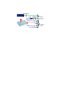
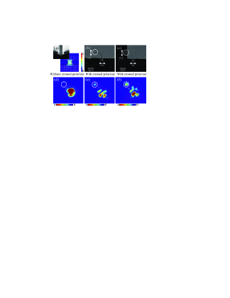
The configuration of the experimental setup is shown in Fig. 1. For excitation, a linearly polarized Gaussian beam (polarization parallel to the antenna) was focused onto the substrate surface. Due to strong back reflection of the incident beam, it is hard to investigate the field in the waveguide unless its direction of polarization is turned so that it becomes visible in the cross-polarized direction. Since the polarization of gap modes is always perpendicular to the tangent of the waveguide, the polarization of the electric fields at the waveguide end can be turned by degrees via a waveguide bend. Thus, the dominant part of the back reflection of the incident beam was filtered out whereas the scattered light from the very end of the waveguide was detected. For comparison, Fig. 2(d) shows the reflection image of the sample surface recorded by a camera without a crossed polarizer in front of the camera. In Fig. 2(e) and (f) two cases with a crossed polarizer in front of the camera are shown. The large bright spot in Fig. 2(d) is caused by the reflection of the focused beam by the nano antenna. On the upper-left side of the reflected beam, there is only a tiny weak spot with strong background noise. However, for crossed-polarizer detection, a small but clear spot can be observed (see spots inside the white-dashed circles in Fig. 2(e) and (f)). This demonstrates that the focused optical beam is coupled to the highly confined mode of the plasmonic waveguide via the resonant receiving antenna. Apparently, cross-polarization detection increases the signal-to-noise ratio (SNR) dramatically. In addition, this proves that we have high transmission through bends with sized radii. The emission intensity with a second transmitting antenna (see Fig. 2(c) and (f)) is enhanced by at least a factor of compared to the case with just an open end (see Fig. 2(b) and (e)). The observed scattering at the end of the waveguide weakens and shifts as expected if the sample is moved relative to the optical beam. For an excitation with an incident polarization perpendicular to the long axis of the antenna, at a non-resonant wavelength or without a receiving antenna (reflection images not presented here), no light is observed at the end of the waveguide.
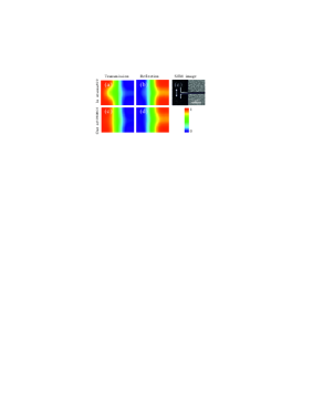
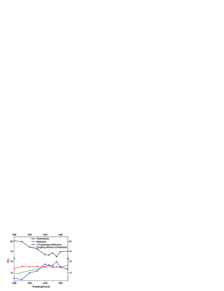
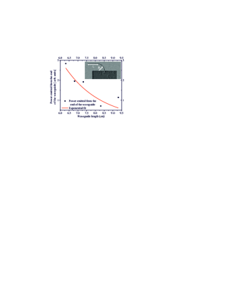
Figure 3 shows scans measured in transmission and reflection at the resonant wavelength of in (a), (b) and at a non-resonant wavelength of in (c), (d). For each scan, the incident polarization was parallel to the antenna. No polarizer was situated in front of the detecting photo diode. Each scanning pixel value corresponds to the normalized transmission and reflection measured for a certain position of the focused beam relative to the sample. The sample was scanned through the beam using a defined step size. Transmission and reflection intensities were measured for every position. All presented scans were normalized to the same level. The transmission for resonant excitation of the antenna is lower (yellow color in Fig. 3(a)) than the value at the non-resonant wavelength (red color in Fig. 3(c)). In the same situation, the reflection does not vary much (see Fig. 3(b) and (d)). This already hints that light is coupled into the waveguide for resonant excitation. We also measured the transmission and reflection spectra of the antenna for incident wavelengths ranging from to (see Fig. 4). The transmission drops by about close to , but the reflection stays almost constant for all measured wavelengths. A quite intuitive explanation suggests that, at resonance, energy is coupled to the waveguide mode and results in a reduced transmission but leaves the reflection almost unaffected. For comparison, we simulated the coupling efficiency using the COMSOL Multiphysics commercial FEM package. In order to get a continuous spectrum, the transient analysis module was used. An excitation port which generated an ultrashort electric pulse (spectral width , central wavelength ) was set at the end of the waveguide far away from the antenna. The detection port with an area of ( grid) was placed above the antenna in air. The powerflow at each point of the detection port in the frequency domain was calculated from the fourier transform of the electric and magnetic fields. The powerflow was then integrated over the detection port area and normalized to the value on the port at the connection between the antenna and the waveguide with an area of . This is to exclude the dispersion effect of the waveguide. Suppose the whole process is reciprocal, we thus obtain the maximum coupling efficiency for an excitation from air. The simulated coupling efficiency shows a maximum around , matching the experimental resonance quite well. Experiments and simulations suggest that about 15% of the beam’s energy is coupled to the waveguide. It should be noted that the calculated coupling efficiency for an excitation from underneath through the substrate is times higher.
Since we were able to control the waveguide excitation, we also determined the decay length of gap modes with a width of at . As shown in Fig. 5, the radius of the bent part (R) is fixed to , and the length of the straight part (L) varies from to . The emission from the waveguide end was used for detection. The light emitted by the waveguide end was extracted and normalized to the power of the optical beam focused on the pure glass substrate. The coupling efficiency of the antenna on each measured sample was maximized by adjusting the position of the nanoantenna relative to the focused beam using a piezo stage. By fitting an exponential decay function to the derived data, the decay length was found to be . The rather low value of the decay length might be due to the fact that the fabricated waveguide width of is expected to be near cutoff. Also the losses of sputtered silver layers seem to be much higher than the values for silver Palik (1985) used in the simulation. Another reason for the low decay length might be that the FIB structuring process introduces roughness on the sidewalls of the gap, which results in additional scattering losses.
In summary, the excitation and detection of plasmonic gap modes has been demonstrated. By using a crossed-polarizer detection scheme that requires bent waveguides, the signal-to-noise ratio was dramatically improved. The excitation of gap modes was shown to be sensitive to the wavelength and position of the excitation beam. The measured sum of the coupling efficiency and antenna absorption reached up to 20% compared to the simulated optimum coupling efficiency of 15%.
The author acknowledges the International Max-Planck Research School (IMPRS) for Optics and Imaging, the Cluster of Excellence for ‘Engineering of Advanced Materials’ (EAM) at the University of Erlangen-Nuremberg and erlangen graduate School in Advanced Optical Technologies (SAOT).
References
- Maier et al. (2005) S. A. Maier, M. D. Friedman, P. E. Barclay, and O. Painter, Appl. Phys. Lett., 86, 071103 (2005).
- Verhagen et al. (2008) E. Verhagen, J. A. Dionne, L. K. Kuipers, H. A. Atwater, and A. Polman, Nano Letters, 8, 2925 (2008).
- Imre et al. (2007) A. Imre, V. K. V. Vlasov, J. Pearson, J. M. Hiller, and U. Welp, Appl. Phys. Lett., 91, 083115 (2007).
- Nomura et al. (2005) W. Nomura, M. Ohtsu, and T. Yatsui, Appl. Phys. Lett., 86, 181108 (2005).
- Chen et al. (2006) L. Chen, J. Shakya, and M. Lipson, Opt. Lett., 31, 2133 (2006).
- Han et al. (2010) Z. Han, A. Y. Elezzabi, and V. Van, Opt. Lett., 35, 502 (2010).
- Bozhevolnyi et al. (2006) S. I. Bozhevolnyi, V. S. Volkov, E. Devaux, J.-Y. Laluet, and T. W. Ebbesen, Nature, 440, 508 (2006).
- Wen et al. (2009) J. Wen, S. Romanov, and U. Peschel, Opt. Express, 17, 5925 (2009).
- Huang et al. (2009) J.-S. Huang, T. Feichtner, P. Biagioni, and B. Hecht, Nano Letters, 9, 1897 (2009).
- Alù and Engheta (2010) A. Alù and N. Engheta, Phys. Rev. Lett., 104, 213902 (2010).
- Mansuripur (1986) M. Mansuripur, J. Opt. Soc. Am. A, 3, 2086 (1986).
- Palik (1985) Palik, Handbook of Optical Constants (Academic, New York, 1985).