Mechanically-Induced Transport Switching Effect in Graphene-based Nanojunctions
Abstract
We report a theoretical study suggesting a novel type of electronic switching effect, driven by the geometrical reconstruction of nanoscale graphene-based junctions. We considered junction structures which have alternative metastable configurations transformed by rotations of local carbon dimers. The use of external mechanical strain allows a control of the energy barrier heights of the potential profiles and also changes the reaction character from endothermic to exothermic or vice-versa. The reshaping of the atomic details of the junction encode binary electronic ON or OFF states, with ON/OFF transmission ratio that can reach up to 104-105. Our results suggest the possibility to design modern logical switching devices or mechanophore sensors, monitored by mechanical strain and structural rearrangements.
pacs:
…Current strategies for miniaturization of logic and memory devices envision the ultimate limit which is the atomic scale control. Several experimental groups have demonstrated the capability of controlling the current flow through single molecular junctions Chen1999 ; Scheer1998 ; Xie2006 ; Nozaki2009 ; Patolsky2004 highlighting promising applications in realms such as nanotechnology and medicine. Outstanding switching properties have been recently revealed in atomic-scale metallic contacts disposed in a three-terminal architecture where the conductance was mechanically switched between “ON” and “OFF” states at room temperature Xie2008 . Other attractive materials such as photochromic organic molecules have been widely used for designing LCD displays and liquid crystals since their transport features can be driven by light irradiation Brakemann2010 or current pulses Zhang2004 . In the quest of designing efficient atomic-scale switching devices, graphene-based materials deserve special attention due to a peculiar one-atom-thick planar geometry combined with exceptional electronic Tan2007 , mechanical and thermal properties Novoselov2004 ; Castro2009 ; Janina2008 . As a result, a wealth of novel phenomena is steadily unveiled in different fields, including spintronics Son2006 , ac transport Rocha2010 ; Prada2009 ; Zhu2009 , or thermoelectrics Zuev2009 .
However, the use of graphene for designing logical switching applications is severely limited by the absence of energy gap. Using advanced lithographic techniques Datta2008 ; Lemme2009 , the fabrication of graphene nanoribbons (GNRs) and band gap engineering have paved the way towards more efficient switching devices. Patterned monolayer graphene nanoconstriction-based field effect transistors were successfully synthesized, confirming that structural confinement can induce energy gap opening and a sharp increase in the ON/OFF ratio (104) Lu2010 . GNRs-based electromechanical and electromagnetic switches were also designed, evidencing the possibility of switching principles of different physical natures Milaninia2009 ; Dragoman2009 . Recently, an efficient and reversible current-induced switching mechanism was reported in large area-graphene based devices, allowing for the design of nonvolatile memory elements Standley2008 . The origin of this switching phenomenon was tentatively related to the formation and breaking of carbon atomic chains bridging two sections of the sample. Additional control parameters can be considered to modulate in a reversible fashion the binary switching properties of molecular junctions. For instance, recent studies have confirmed that mechanical strain can effectively monitor the electronic structure and transport response of carbon-based materials Quek2009 ; Ni2009 ; Poetschke2010 ; Mohiuddin2009 ; Pereira2009 . In particular for graphene that are gapless materials, the use of mechanical forces as control parameters can establish important strategies for envisioning band gap engineering in graphene structures.
Despite all these efforts to develop and monitored switching devices, the understanding of intrinsic operating mechanisms and their relation with the atomic-scale features are open issues demanding for advanced theoretical investigation. In particular, there is a need to investigate the deep connection between reversible modifications occurring at the atomic-scale and the resulting electronic behavior of devices exposed to external perturbations Agapito2007 ; Yin2009 ; Hashimoto2004 ; Yakobson2000 . In this Letter, the inherent switching mechanism of physical reactions involving graphene etched junctions is dynamically probed using theoretical simulations. Our goal is to identify optimum physical conditions for tuning the conductance between binary switching states. A physical reaction is simulated by examining the potential profile on the coordination axis of the rotating carbon dimers under applied mechanical stress needed for improving the switching features of the device. The associated activation energy for the reaction and its ground state are determined by the derivation of minimum energy paths (MEP). Mechanical strain is subsequently used to modulate the energy onsets and barrier heights which characterize the structural transition. Regarding the transport response of the system, we establish clear thresholds between ON and OFF states as we monitor their electronic transmission along the whole reaction path. Prominent switching behaviour can be achieved depending on the atomic widths of the nanostructures and amount of applied strain. Our findings ensure a promising way for designing ultimate molecular switching devices based on strained graphene. We also extend graphene’s applicability to another scientific frontier which is the production of mechanophore sensors based on etched graphene samples. Such special materials consist of systems where their reaction path depends on the strength and nature of the applied force Arino2010 .
Minimum energy path results: In what follows, we performed systematic analysis of transport properties and mechanical activity of two different graphene constrictions where carbon dimers bridge the gap between two semi-infinite graphene ribbons. Here we refer as a bi- (tri-) switch configuration, the constriction with two (three) C-C bonds linking the graphene segments. A minimum energy path which resolves the system undergoing a structural rearrangement of atoms can be tracked assuming two metastable configurations: a graphene nanojunction made by pure hexagons (initial state) and a defective constriction composed of pentagon-heptagon pairs (final state). The variable is associated to the normalized reaction coordinate where corresponds to the initial anchor state and defines the ending of the reaction. Ball and stick schematic pictures for initial, intermediate and final states are displayed in Fig. 1, panels (a) and (b). The physical reaction consists of rotating the C-C bonds located on the “neck” of the initial hexagonal junction by 90∘, generating rings of Stone-Wales defects in the final configuration. After the rotation, we observe that the optimal lattice constant along the axial direction suffers a small expansion of 0.7 Å, characterizing an endothermic-like reaction. The transition route linking these two configurations states can be located using nudged elastic band (NEB) method Henkelman2000 . The method gathers the MEP by constructing a set of replicas of the system between the initial and final states. A spring interaction between consecutive images is included to ensure the continuity of the path. Optimization procedures that minimize the forces acting on the images are implemented to obtain the MEP.
Our results obtained for the two switching systems are shown in Fig. 2. The total energy variation along the whole trajectory are mapped as a function of the reaction coordinate () and the reference energy for the initial state is set to 0 eV. The structures are also submitted to uniaxial mechanical forces under DFTB frame Xu92 and we demonstrate the ability of controlling the MEP profiles by applying such perturbation. A schematic representation of the applied forces is shown in Fig. 1 (c). We applied mechanical strain by pulling away the atoms located at upper and lower edges at incremental values and further fixing them. The atomic geometries except for the edge constrained atoms are subsequently relaxed under the conditions of NEB method. The equivalent mechanical energy resulting from the stretching is defined as , being the external force and , with and the deformed and initial equilibrium lattice constant parameters along the axial direction, respectively. The strain is calculated as .

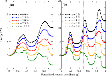
For unstrained systems, the ground state for both switching systems is the initial hexagonal junction. For bi-switching configuration, two humps can be observed along the reaction path while three others appear for tri-switching arrangement. Each one of those humps is associated to the amount of energy required to rotate one C-C bond by 90∘ in the junction. After the rotation, we observe that the optimal lattice constant along the axial direction suffers a small expansion of %, characterizing an endothermic reaction. The energy barrier heights for the complete transition are estimated as 12.4 eV and 16.8 eV for bi-switching and tri-switching structures, respectively. The barrier heights as well as the energies of initial/final configurations can be strongly modulated with the aid of mechanical strain. From the pictures, we can see that the barrier heights are considerably reduced as stretching takes place. At tensile strains of 7.5% (6%) for bi- (tri-) switching structure, the barrier heights for both structures decrease from 12.4 eV (16.8 eV) to 4.0 eV (4.8 eV), and the anchor states are set almost evenly in energy. As the mechanical strain continues to increase, the ground state is switched from the hexagonal junction to the 5-7 defective configuration and the reaction becomes exothermic-like. The formation of 5-7 defect lines reduces the number of the bonds connecting the two graphene segments and this dwindles the energy loss in response to the elongation.
Up to this point, we evidenced that the physical reactions involving graphene junctions under strains of 6%-7.5% are energetically favorable to be triggered since the total energies of initial and final states are comparable and the barrier heights are considerably reduced. We now explore if such strained systems reveal optimum switching behaviour through electronic structure analysis. This issue is investigated by following how the electronic structure and transport responses change along the reaction coordinate path. The efficiency of standard logical switches can usually be measured through the magnitude of ON/OFF transmission rates, controlled by gate voltages. In our case, the reaction coordinate that resolves the dynamic trajectory between the anchor states, acts as an additional switching parameter. In this sense, prominent switching responses can also be dynamically tuned as the system evolves along the MEP. An efficient dynamic switch is characterized by finding pronounced differences between the transmission values taken from the initial and final configurations. To represent the electronic structure of both extreme states, we adopted self-consistent-charge Density Functional based tight binding theory (DFTB) Elstner1996 ; Seifert1996 and the conductance was subsequently calculated using Landauer formula written in terms of Green’s functions Nardelli1999 .
Figure 3 depicts the energy relation dispersions calculated for initial [(a) and (c) panels] and final states [(b) and (d) panels] for bi-switching (upper panels) and tri-switching (lower panels) systems. The Fermi energy is set at 0 eV. The atomic arrangement along the edges of both junctions follows a zigzag shape and hydrogen atoms are used to saturate dangling bonds situated outside the constriction domain. The non-saturated dangling bonds give raise to flat bands at the Fermi level. This can be confirmed through the electronic wave function plots displayed on the lower panels (g) and (h) for the tri-switching example. The wave functions are calculated at the point for energies around eV. In fact, the electronic distribution is highly concentrated on the edges. Such bands are rather robust and do not respond to the structural modification of rotating carbon dimers. This indicates that favorable switching features cannot be achieved at eV for both nanojunctions.
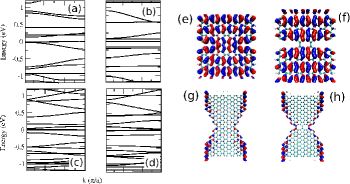
For the bi-switching arrangement, outstanding switching properties can be highlighted in the energy range of eV. The subband dispersion within this range shown on panel (a) is considerably reduced as the bonds rotate, characterizing a potential transition between ON [panel (a)] and OFF [panel (b)] states. To rationalize these findings, the electronic wave functions calculated at the point are shown for particular energies in the bi-switching example [(e) and (f) lower panels]. We observe a highly delocalized spatial distribution of conduction channels for the initial frame whereas two disconnected orbital patterns are obtained at the ending of the reaction. Rotating the horizontal C-C bonds of the hexagonal bi-switching junction disrupts the superposition of the molecular orbitals on the constriction. The system behaves, then, as two isolated semi-infinite graphene sections and the electronic channel is blocked. On the other hand, the electronic structure of tri-switching arrangement seems to exhibit weaker switching behaviour. Comparing the energy relations displayed on panels (c) and (d), one can see a significant resemblance within the whole spectrum which means that the structural reaction does not cause significant impact on the electronic response of such junctions.

The precise evaluation of the ON/OFF transmission rates is obtained through Fig. 4 which shows the conductance contour plots as a function of the Fermi energy and reaction coordinates obtained for both strained samples. The results reveal once more the excellent binary switching behaviour of bi-switching structure in contrast to tri-switching case. The gradient color located on the energy range of eV unveils a gradual exchange between ON (red color) and OFF (blue color) states with respect to the reaction coordinate path. The maximum transmission rate is determined as 104-105. Assuming that the final state can be stabilized, the transition between high and low transmission states can also be induced through the use of some external gate voltages. Differently, tri-switching configuration manifests a robust transport response with minor changes appearing in the same energy range. Lower transmission values are evidenced only for a few intermediate reaction frames indicating that the weaker switching capability of such system can be better manipulated via gate voltages.
Conclusion: We reported the manifestation of binary switching behaviour on graphene nanojunctions that experience a physical reaction capable of rearranging locally the atomic structure of the systems. The junctions are also exposed to uniaxial mechanical stretching which tunes the physical characteristics of the reaction such as energy barrier heights and ground state. As the reaction occurs, we observe that narrower junctions reveal promising ON/OFF transmission rate reaching values up to 104-105 which is in agreement with current experimental measurements performed in graphene nanoconstrictionsLu2010 . Our results also support the interpretation of recent experiments carried on atomic quantum transistors where self-stabilizing contact reconstruction can be mechanically driven Xie2008 .
Acknowledgments. This work was partially funded by Alexander von Humboldt Foundation, the European Union, the Free State of Saxony (SAB project number A2-13996/2379) and the NANOSIM-GRAPHENE Project No. ANR-09-NANO-016-01 and the South Korean Ministry of Education, Science, and Technology Program, Project WCU ITCE No. R31-2008-000-10100-0.
References
- (1) J. Chen, et al., Science 286, 1550 (1999).
- (2) E. Scheer, et al., Nature 394, 154 (1998).
- (3) F.-Q. Xie, Ch. Obermair and Th. Schimmel, NATO Sci. Series II: Math., Phys. and Chem. 233, 153 (2006).
- (4) D. Nozaki and G. Cuniberti, Nano Res. 2, 648 (2009).
- (5) F. Patolsky, et al., Proc. Natl. Acad. Sci. USA 101, 14017 (2004).
- (6) F.-Q. Xie, et al., Nano Lett. 8, 4493 (2008).
- (7) T. Brakemann, et al., J. Bio. chem. 285, 14603 (2010).
- (8) C. Zhang, et al., Phys. Rev. Lett. 92, 158301 (2004).
- (9) Y. W. Tan, et al. S. Adam, E. H. Phys. Rev. Lett. 99, 246803 (2007); A. Lherbier, B. Biel, Y.-M. Niquet, and S. Roche, ibid. 100, 036803 (2008).
- (10) K.S. Novoselov, et al. Morozov, D. Jiang, Y. Science 306, 666 (2004).
- (11) A.H. Castro Neto, et al., Rev. Mod. Phys. 81, 109 (2009); M. Lemme, Sol. Stat. Phenom. 156-158, 499 (2010).
- (12) J. Zimmermann, P. Pavone, and G. Cuniberti, Phys. Rev. B 78, 045410 (2008).
- (13) Y.-W. Son et al., Nature (London) 444, 347 (2006); S. Lakshmi, S. Roche, and G. Cuniberti, Phys. Rev. B 80, 193404 (2009);
- (14) C. G. Rocha, L. Foa Torres, and G. Cuniberti, Phys. Rev. B 81, 115435 (2010).
- (15) E. Prada, P. San-jose, and H. Schomerus, Phys. Rev. B 80, 245414 (2009).
- (16) R. Zhu, and H. Chen, Appl. Phys. Lett. 95, 122111 (2009).
- (17) Y.M. Zuev, W. Chang, and P. Kim, Phys. Rev. Lett. 102, 096807 (2009);
- (18) S.S. Datta, D.R. Strachan, S.M. Khamis, and A.T.C. Johnson, Nano Lett. 8 1912 (2008).
- (19) M.C. Lemme, et al., ACS Nano 3, 2674 (2009).
- (20) Y. Lu, B. Goldsmith, D.R. Strachan, J.H. Lim, Z. Luo, A.T.C. Johnson, Small 6, 2748 (2010).
- (21) K.M. Milaninia, M.A. Baldo, A. Reina, and J. Kong, Appl. Phys. Lett. 95, 183105 (2009).
- (22) M. Dragoman, D. Dragoman, F. Coccetti, R. Plana, and A. A. Muller, J. Appl. Phys. 105, 054309 (2009).
- (23) B. Standley, et al., Nano Lett. 8, 3345 (2008).
- (24) S. Y. Quek, et al., Nat. Nanotech. 4, 230 (2009)
- (25) Z.H. Ni, T. Yu, Y.H. Lu, Y.Y. Wang, Y.P. Feng, and Z.X. Shen, ACS Nano 3, 483 (2009)
- (26) M. Poetschke, C.G. Rocha, L.E.F. Foa Torres, S. Roche, and G. Cuniberti, Phys. Rev. B 81, 193404 (2010);
- (27) T. M. G. Mohiuddin, et al., Phys. Rev. B 79, 205433 (2009).
- (28) V. M. Pereira, and A. H. Castro Neto, Phys. Rev. Lett. 103, 046801 (2009); V. M. Pereira, N. M. R. Peres, and A. H. Castro Neto, Phys. Rev. B 80 045401 (2009).
- (29) L. A. Agapito, and H.-P. Cheng, J. Phys. Chem. C 111, 14266 (2007).
- (30) C. Yin, et al., J. Chem. Phys. 131, 234706 (2009).
- (31) A. Hashimoto, K. Suenaga, A. Gloter, K. Urita, and S. Iijima, Nature 430, 870 (2004).
- (32) B. I. Yakobson, G. Samsonidze, and G. G. Samsonidze, Carbon 38, 1675 (2000).
- (33) J.R.-Arino, M. Shiga, and D. Marx, J. Am. Chem. Soc. 132, 10609 (2010)
- (34) G. Henkelman, B.P. Uberuaga, and H. Jónsson, J. Chem. Phys. 113, 9901 (2000)
- (35) C.H. Xu, C.Z. Wang, C.T. Chan, and K.M. Ho, J. Phys. Condens. Matter 4, 6047 (1992)
- (36) M. Elstner, et al., Phys. Rev. B 58, 7260 (1998)
- (37) G. Seifert, D. Porezag, and T. Frauenheim, Int. J. Quantum Chemistry 58, 185 (1996)
- (38) M. Buongiorno Nardelli, Phys. Rev. B 60, 7828 (1999)