Low-temperature tapered-fiber probing of diamond NV ensembles coupled to GaP microcavities
Abstract
In this work we present a platform for testing the device performance of a cavity-emitter system, using an ensemble of emitters and a tapered optical fiber. This method provides high-contrast spectra of the cavity modes, selective detection of emitters coupled to the cavity, and an estimate of the device performance in the single-emitter case. Using nitrogen-vacancy (NV) centers in diamond and a GaP optical microcavity, we are able to tune the cavity onto the NV resonance at 10 K, couple the cavity-coupled emission to a tapered fiber, and measure the fiber-coupled NV spontaneous emission decay. Theoretically we show that the fiber-coupled average Purcell factor is 2-3 times greater than that of free-space collection; although due to ensemble averaging it is still a factor of 3 less than the Purcell factor of a single, ideally placed center.
pacs:
42.50.Ex, 78.66.Fd, 42.82.Et, 61.72.jn1 Introduction
Several properties of the negatively-charged nitrogen-vacancy center (NV-) in diamond make it an attractive candidate as a qubit for quantum information processing (QIP). First, the ground-state electron-spin decoherence time exceeds a millisecond in isotopically purified 12C diamond samples [1]. Second, an excited-state manifold [2, 3] provides optical access to both initialize and control the electron ground-state spin [4, 5] as well as a way to create quantum entanglement through photon interference [6]. Finally, hyperfine coupling of the electron spin to either N or 13C nuclear spins [7, 8] provides access to a second storage qubit needed for quantum protocols based on repeat until success schemes [9, 10].
The majority of NV- experiments have been performed on NV centers found deep within the diamond substrate utilizing free-space excitation and collection optics. There is now significant motivation to integrate these quantum emitters into optical devices to build scalable measurement-based optical quantum networks. To realize these networks coupling NV- centers to optical cavities will be necessary to enhance emission into the zero-phonon line (ZPL) [11] and for coupling ZPL emission into waveguides for efficient collection. NV-cavity coupling can be obtained by coupling NV centers in diamond nanoparticles to non-diamond microcavities [12, 13, 14, 15], coupling NV centers in single-crystal diamond to non-diamond cavities (hybrid approach) [16, 17], and by fabricating microcavities out of single-crystal diamond (all-diamond approach) [18, 19, 20, 21]. Due to the poor spectral properties of NV centers found in nano-diamond, the first approach is challenging for scalable optical networks that rely on interference for ‘which-path’ erasure. Of the single-crystal diamond approaches, the all-diamond approach has the advantage of a higher optical field strength at the NV site which lies within the cavity structure, and significant enhancement of the NV emission into the ZPL has already been observed in all-diamond microrings [18]. The hybrid approach, which relies on coupling diamond NVs to the evanescent field extending out of the non-diamond cavity, has the potential advantage of additional device functionality provided by the material properties of the waveguide layer. For example, the electro-optic properties of the cavity material could enable switching or cavity tuning capabilities.
A figure of merit for the coupling between a cavity mode and dipole emitter is the spontaneous emission enhancement (Purcell) factor . For an emitter at position in a monolithic cavity and on resonance with the cavity mode,
| (1) |
in which is the vacuum wavelength, is the cavity refractive index, is the cavity mode quality factor, is the cavity mode volume, is the electric field strength at the dipole, and is the maximum electric field strength. There are several key device factors that must be optimized. The optical cavity quality factor must be sufficiently large and its mode volume sufficiently small. The quantum emitter must be coupled spatially to the cavity mode and spectrally on resonance. Finally, in addition to cavity-dipole coupling, the cavity mode must be efficiently coupled to a useful input/output mode (i.e. a waveguide).
When engineering optical devices for QIP applications, device testing becomes prohibitively difficult when all testing must be done on single emitters. This is especially true in the common case where the spectral and spatial properties of the emitter are difficult to control. In this work we develop a test platform based on emitter ensembles designed to evaluate coupled emitter-cavity performance. This platform is particularly useful for hybrid-type devices in which the material properties of the waveguide layer may need to be tested before investing the resources necessary to test single-emitter devices.
In this work we focus on coupling an ensemble of near-surface NV- centers in single crystal diamond to GaP micro-cavities fabricated through photolithographic and dry-etching techniques. We show that it is possible using a tapered fiber to collect emission preferentially from centers that are coupled to the cavity [22, 23]. We are able to deterministically tune the cavity resonance several nanometers onto the NV- ZPL and perform lifetime measurements using the photoluminescence (PL) collected through the tapered fiber. The lifetime measurements can be used to evaluate NV-device coupling. Although we are experimentally unable to observe a significant reduction in the ensemble lifetime for these particular devices, we demonstrate the feasibility of the testing method and theoretically show that there is a significant advantage to using the tapered fiber over free-space collection in ensemble measurements.
2 Hybrid GaP-diamond cavity fabrication
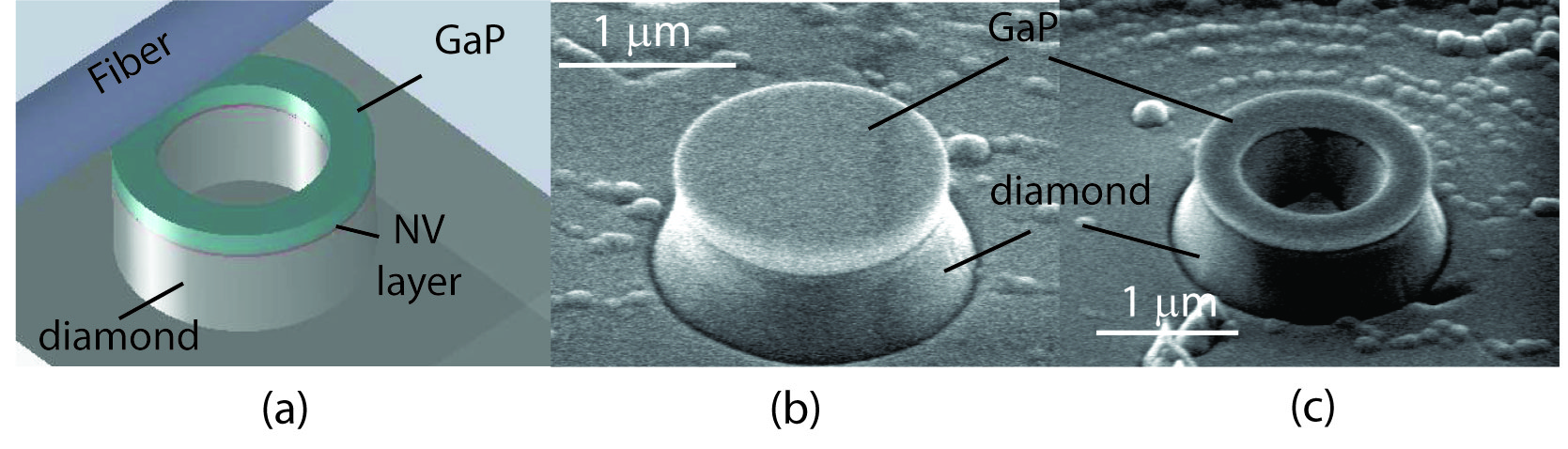
The tested devices consisted of a GaP microcavity on top of a diamond pedestal with an ensemble of NVs near the diamond surface (Fig. 1a). GaP has a refractive index of that is higher than that of diamond (), and it is transparent at 637nm, the ZPL wavelength. Thus devices made from GaP on diamond can support high-Q modes that couple evanescently to the NV centers near the diamond surface.
Experiments were performed on a a commercially available type IIa (110)-oriented diamond chip (Element 6) grown by chemical vapor deposition (CVD) with a nitrogen concentration of [N]1 ppm as specified by the manufacturer. The NV ensemble was created by N+ ion implantation at 10 keV (CORE Systems) at a dose of cm-2 followed by a one hour high temperature anneal at 900 ∘C in a H2/Ar forming gas. To maximize the fraction of NV centers in a negatively-charged state, the sample was further annealed in an oxygen atmosphere at 465 ∘C for 2 hours [24]. In this sample there are three mechanisms of NV formation. First, NVs are incorporated during the CVD growth process. The density of these NVs is expected to be less than cm-3 [25] and thus their contribution to the total collected signal can be neglected. A second way an NV is formed is when a vacancy created by the implantation process diffuses and is trapped by a native nitrogen during the annealing process. The maximum NV density due to this process is 2 cm-3 based on electron irradiation studies aimed at maximizing the NV- yield in similar CVD material [25]. These NVs are located within the first 200 nm of the surface [26] and have a maximum sheet density of cm-2. Finally, an NV can form when a vacancy is trapped by implanted nitrogen. This third type of NV is expected to be nm from the surface, as estimated using SRIM [27]. The estimated sheet density is cm-2 assuming a 10% conversion rate of implanted ions to NV- which is typical in our devices. Even for free-space collection the majority of the NV PL signal is due to the implanted nitrogen. By using a tapered fiber we are able to further select NVs which are coupled to the cavity. We note that if an electronic-grade CVD diamond substrate ([N]1 ppb) were used only the third type of NV would be present.
The starting material for the GaP microcavities was a commercially available (IQE) wafer consisting of a 250 nm GaP layer on an 800 nm Al0.8Ga0.2P sacrificial layer grown by molecular beam epitaxy. For one set of devices the original 250 nm thickness was used while in a second set the GaP layer was thinned by dry etching to 150 nm. The microcavities were defined photolithographically using a mask consisting of 1.5-3 m diameter disks. The resist mask (SPR-955) was reflowed on a hotplate at 180 ∘C and was used as an etch mask in an Ar/BCl3/Cl2 reactive ion etch (RIE) chemistry. By varying the optical exposure time it was found that rings could also be produced due to diffraction around the disk mask.
As a further step to facilitate tapered-fiber testing, a 20 m tall, 190 m wide diamond ridge defined by a SiN mask was etched on the diamond surface using an O2/Ar RIE chemistry. The GaP microcavities were then transferred to the diamond ridge using the probabilistic “drop-down” method described in Ref. [16]. This procedure provides an easy shortcut for testing single devices, but eventually this must be replaced with a wafer-bonding approach before integrated photonic networks can be constructed. After transfer the devices were etched in an oxygen RIE plasma to create a 600 nm diamond pedestal beneath the GaP disks. This pedestal improves the lateral confinement of the cavity modes, decreasing radiation loss into the diamond substrate [28].
Scanning electron microscope images of the two devices studied for this work are shown in Fig. 1b,c. Device D1 consisted of a 250 nm thick, 1.5 micron diameter GaP disk and device D2 consisted of a 150 nm thick, 280 nm wide, ring waveguide with a 1.6 m outer diameter. These devices were examples of the smallest devices made and had cavity resonances within tuning distance of the NV- ZPL.
3 Tapered-fiber coupling to high-index cavities
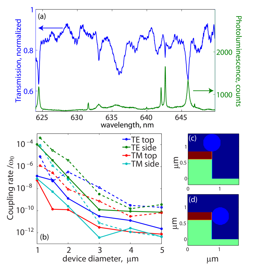
A 550 nm nm diameter tapered fiber was used to collect NV photoluminescence from the hybrid GaP-diamond cavities. The tapered fiber position was controlled by a piezo stage and contacted to the top or side of the GaP microcavity to collect NV photoluminescence as shown in Fig. 1a. Room-temperature transmission measurements were performed to characterize the fiber-microcavity coupling. Only in the smallest disk devices (sub-2 m diameter) could transmission dips be observed as shown in Fig. 2a. Transmission dips ranging from a few percent to a few tens of percent could be attained. The utility of using a tapered fiber for device evaluation depends critically on the collection efficiency, especially in the case of single centers. We have thus estimated the energy decay rate from the cavity mode into the waveguide as a function of device diameter numerically using coupled mode theory.
We first simulated the uncoupled lowest order TE and TM cavity modes for disk and ring devices using FDTD (MEEP [29]). The fiber mode was calculated using well-known analytic expressions for a step-index circular waveguide [30]. The fiber diameter was taken to be 550 nm and the fiber index = 1.45. In Ref. [31], an expression for the coupling rate between a cavity mode and fiber is derived using power conservation. Using this formalism, one can show that the total decay rate of energy from the cavity into the fiber is given by
| (2) |
where and are the cavity and fiber electric fields, respectively, and is the resonant frequency. The 2D integral is taken over the fiber cross section and the 1D integral is along the fiber propagation axis with at . We have assumed that the cavity mode is a standing wave which decays equally into both forward and backward propagating waveguide modes. The cavity field is normalized to unit energy [32],
and the waveguide field is normalized to unit power,
() is the cavity (fiber) magnetic field and is the dielectric constant.
The results of the coupled-mode calculation are shown in Fig. 2b for both ring and disk devices for a fiber in contact with the top of the device (Fig. 2c) and for a fiber in contact with the side of the device (Fig. 2d). Experimentally there is uncertainty in the fiber-cavity contact position, the extent of the fiber-cavity contact, the fiber diameter, and the the phase of the standing-waves. Even with these uncertainties the simulations do provide some insight into how to achieve the best fiber-device coupling. As the device diameter becomes smaller it appears easiest to couple to the TE modes from the side of the disk. The ring device in general provides better coupling due to the thinner GaP layer. If we assume a reasonable cavity Q of 10,000, appreciable coupling (decay rate due to the taper is greater than 10% of the uncoupled decay rate) only occurs for device diameters less than 1.5 m. To be able to attain critical coupling in these geometries the device diameter would need to be sub-micron. Such small devices are desirable for large Purcell factors and could be fabricated using electron-beam lithography. There is however a fundamental limit on the minimum device diameter before Q is limited by radiation loss, . FTDT calculations show that for GaP-diamond hybrid devices this diameter can be quite small: for a 150 nm GaP layer nm and for a 250 nm layer nm.
4 Fiber collection of the cavity-coupled zero-phonon emission at 10K
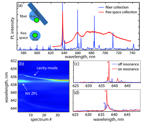
NV photoluminescence spectra collected in free space from the center of disk D1 and collected through a tapered fiber coupled to the whispering-gallery modes of the cavity are shown in Fig. 3a. In all PL measurements the NV centers are excited with 532 nm excitation. In the free space spectrum, excitation and PL collection is from the top of the disk through a 0.55 numerical aperture objective. The NV- ZPL line is observed at 637 nm with a 1.5 nm inhomogeneous linewidth. This inhomogeneity is generally observed in heavily implanted samples and could be a result of strain introduced during the implantation process. In the tapered fiber spectrum the disk is excited at its edge and the excitation spot is spatially separated from the tapered-fiber contact position. This is to reduce scatter from uncoupled NVs into the tapered fiber. The sharp cavity modes can clearly be observed over the background PL with a contrast greatly exceeding what can be achieved in free-space using spatial filtering [16].
Due to variations in device fabrication, it is unlikely that a cavity mode will initially be on resonance with the 637nm zero-phonon emission. Temperature tuning is not useful in this system because the ZPL becomes phonon broadened at temperatures greater than 15 K [33]. Instead we tune the cavity by injecting xenon gas into the cryostat which condenses on the microcavity and alters its mode volume [34]. Microdisk resonance tuning up to approximately 3 nm is possible for these GaP devices which have a free spectral range exceeding 20 nm. It is thus necessary to fabricate many devices to ensure a subset of devices is within the tuning range. Fig. 3b depicts a series of PL spectra from device D2 as Xe is continuously leaked into the cryostat. An increase in the PL intensity as the cavity is tuned onto the ZPL resonance is observed. A comparison between the on-resonance and off-resonance fiber spectra for both D1 and D2 are shown in Figs. 3c,d showing a marked enhancement in the ZPL collection in the resonant case. Quality factors of 4900 and 3500 were measured for D1 and D2 respectively.
5 Lifetime measurements of cavity-coupled NV centers
The NV-cavity coupling strength can be determined from changes in the spontaneous emission lifetime that occur when the NV ZPL is resonant with the cavity mode. The decay rate for a single NV center prepared in a particular excited state may be written as,
| (3) |
where is the total uncoupled decay rate including nonradiative channels as well as spontaneous emission through other modes, is the zero-phonon spontaneous emission rate in bulk diamond, and is the Purcell factor. In high-quality diamond samples typically , but in the present samples we observe , suggesting a strong non-radiative component. We have previously measured of the total NV- photoluminescence intensity including the phonon sidebands which is consistent with the literature [35]. If represents a fraction of the total uncoupled decay rate then the ratio of the on-resonance lifetime to the uncoupled lifetime would be
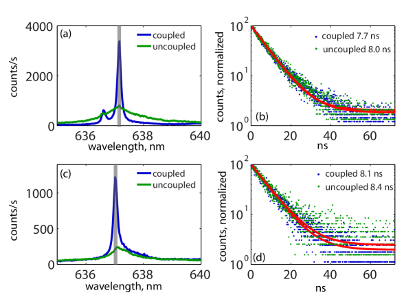
Using the tapered-fiber collection, we measure the SE decay curve of the cavity-coupled NV ensemble. This measurement, combined with a theoretical consideration of the effects of ensemble averaging, can be used to estimate the spontaneous emission enhancement of a single NV center with a particular position and orientation, as is discussed below. Prior to performing ensemble lifetime measurements the cavity was tuned to the ZPL resonance. NV emission was collected through the fiber using the geometry depicted in Fig. 3a. PL spectra under continuous-wave excitation of NVs in both the disk D1 and ring D2 devices are shown in Fig. 4a,c. For the lifetime measurements, a green pulsed excitation source was used, based on supercontinuum generation with a Ti-Sapphire laser. The excitation source had a bandwidth of 28 nm centered at 520nm and a repetition rate of 4.75 MHz. The ZPL emission was filtered as depicted by the shaded regions in Fig. 4a,c. The SE decay curves for devices D1 and D2 were fitted to a single exponential with decay times of ns and ns respectively (Fig. 4b,d). The measurement was repeated on NV centers that were not coupled to the cavity mode. To collect uncoupled emission the fiber was placed across the center of the device and the NV centers directly under the fiber were excited. As seen from the PL spectra in Fig. 4a,c, in this excitation/collection geometry the ZPL line is weak and broad and thus shows no features of the cavity mode. Lifetime measurements of uncoupled NVs yielded characteristic decay times of ns and ns for D1 and D2 respectively. We show below that this lifetime reduction is somewhat smaller than what is expected theoretically.
6 Simulated lifetime modification
Next, let us discuss the lifetime modification expected theoretically for a large ensemble of NV centers coupled to the cavity modes of device D2. Each NV center has a number of characteristics that affect its excited-state dynamics, including its position relative to the cavity mode, the orientation of the N-V axis along one of the four axes, the principle axes of symmetry breaking for the two excited orbital states as determined by local strain or electric fields, and the frequency shifts of the optical transitions, again determined by local fields. Nonradiative decay channels may also be present, including decay through the singlet states (especially from the spin sublevels [36]).
To simplify the discussion, here we neglect the dynamics of the spin sublevels, and consider only the two orbital excited states. Such an approximation is not suitable for a detailed analysis of NV dynamics, but suffices to illustrate the effect of spatial and orientational inhomogeneity on the radiative dynamics. Under this simplification we can use Eq. 3 to model the decay rate for a single NV center prepared in a particular excited state , and we let . The Purcell factor is given by,
| (4) |
which is similar to Eq. 1 except that we have included the factor of necessary for the hybrid geometry and also the effect of dipole alignment and spectral detuning. Here, is the diamond refractive index and is a unit vector parallel to the relevant transition dipole moment. The hybrid-cavity mode volume is given by
in which is the dielectric constant at the location of the field maximum [11]. The NV center has two optical transitions involving the two orbital excited states with dipole moments orthogonal to the N-V axes. The principle axes [37, 38] can be described in terms of an angle ; for example for an NV oriented along , the dipole moments are and , where and . If the angle is determined by local fields then we expect it to be randomly distributed, and here we assume a uniform distribution. It is important to note that we neglect population relaxation between orbital excited states. This assumption is reasonable only for measurements performed at liquid-helium temperatures [33]. We further assume that the two orbital excited states have the same unmodified decay rate. In general, we must also include the effect of detuning, and here is the detuning between the dipole transition frequency and the central frequency of the cavity mode, while is the cavity linewidth. In the measurement, we detect photoluminescence through a spectral filter of bandwidth centered at the cavity frequency, and therefore we detect emission only from a subset of NV transitions that are nearly on resonance with the cavity mode. Thus we set for the present calculation.
While our model assumes a simple exponential decay for each NV transition, the ensemble-averaged behavior is non-exponential, but can be written as,
| (5) |
where is the measured PL decay curve, and represents a distribution of NV transitions with various Purcell factors, decaying at various rates, weighted by their relative occurrence and by their excitation and collection efficiencies. For free-space collection this distribution can be written as,
| (6) |
Here, is the N-V orientation vector, and is the NV density with respect to position and dipole orientation. For the spatial dependence, we approximate as a Gaussian distribution with respect to depth below the surface, with a mean depth of and variance (straggle) of . Such a distribution corresponds to a uniform nitrogen ion implantation as estimated using SRIM [27], assuming that the resulting NV centers incorporate only implanted nitrogen, and that the implanted nitrogen does not diffuse during annealing. The excitation efficiency includes a spatial dependence that is modeled as a diffraction-limited Airy disk pattern corresponding to excitation through a 0.55 numerical-aperture lens (), centered between the inner and outer edges of the ring structure. The excitation efficiency is also assumed to be proportional to , where the excitation polarization is along .
For collection through the tapered fiber, Eq.6 must be modified since, ideally, only light emitted into the cavity mode of interest is collected. Thus we weight by the emission rate into the cavity mode, which is proportional to the Purcell factor:
| (7) |
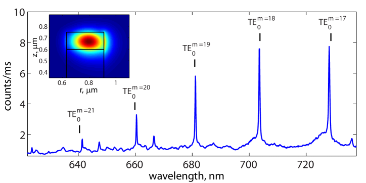
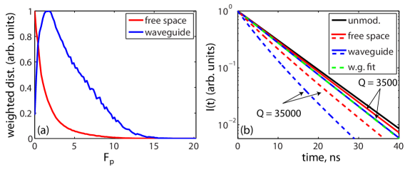
The lowest-radial order TE cavity field was simulated for the calculation using FDTD (MEEP) software [29]. A reasonably good agreement between the experimental and simulated resonance frequencies could be obtained for a model device with a 1.8 m outer diameter as shown in Fig. 5. Using the parameters given above, setting and considering a single standing-wave cavity mode (rather than degenerate counter-propagating modes) we obtain the Purcell-factor histograms shown in Fig. 6a. For this mode the maximum expected Purcell factor for an NV 15 nm below the surface and with perfect dipole alignment is . However, for free-space collection the weighted average is only . For collection through the tapered fiber, because we preferentially detect NV centers that are better coupled to the cavity mode, the average increases to . But even with the tapered fiber it is clear that the random spatial and angular distributions of dipole moments reduces the mean cavity enhancement by a large amount.
For a more direct comparison with experiment, PL decay curves generated from these distributions are shown in Fig. 6b. Here we have assumed to match the behavior observed in these heavily implanted samples, and , as discussed above. Although these decay curves do not follow a single-exponential time dependence, because the average decay modification is weak compared with , it would be quite difficult experimentally to detect the deviation from single-exponential behavior caused by variations in . The effective decay lifetimes obtained by fitting the first of decay to a single exponential are and for free-space and tapered-fiber collection, respectively. These are approximately equal to those expected from the values given above: and for free-space and tapered-fiber collection, respectively. Fig. 6b also includes simulations for a device with Q = 35000. Q’s exceeding 25000 have been observed previously in much larger hybrid GaP-diamond devices [16] and more work is required in determining the factors limiting the Q in the present devices.
The lifetime modification shown in Fig. 4, which was at the limit of detection, is smaller than that predicted in this simulation, and some likely causes include the presence of an air gap between the GaP ring [40] and the diamond surface, or non-ideal NV distributions. The simulations show that collection using the tapered fiber provides an important advantage since it selectively filters out NV centers that are poorly coupled to the cavity. Nevertheless, even using the tapered fiber for collection, ensemble averaging reduces the effective Purcell factor by a factor of approximately 3 compared with that expected for an ideally positioned and oriented NV center.
7 Outlook
There is significant motivation to integrate photonics with quantum systems for quantum communication, quantum information interfaces, and for quantum information processing. In final devices, quantum-photonic ”nodes” will consist of single emitters, however single emitters are challenging to work with when studying and developing the classical photonic networks. Here we presented a method combining an ensemble of emitters and tapered-fiber collection which can be used for fast serial testing of a large number of QIP devices.
Experimentally we showed that tapered-fiber collection provides a way to obtain high-contrast spectra to reliably observe cavity modes. This is because the fiber enables the selective detection of NVs coupled to the cavity. Compared to a free-space collection, the measurement more directly probes the signal that would be collected by an on-chip waveguide, as part of an integrated photonic network. Although not exploited in this work, variable coupling is also possible with the tapered fiber providing a way to optimize the combined cooperativity parameter that includes both and the waveguide-cavity coupling efficiency. Additionally, numerical calculations indicate that for sub-micron GaP-diamond hybrid devices, the cavity energy decay rate into the fiber should be able to exceed the uncoupled decay rate allowing for efficient photon collection.
The use of NV ensembles provides two main advantages over single centers for device testing. First, the collected photoluminescence can be much greater allowing for faster testing. Second, device characterization does not rely on nanometer-scale placement of single emitters. Although the devices used to test this platform did not exhibit a significant Purcell enhancement, theoretically we showed that the fiber-coupled average Purcell factor is 2-3 times greater than that of free-space collection. Moreover, if the distribution of emitters is known, the ensemble device performance can also be used to estimate the single-emitter device performance.
This material is based upon work supported by the Defense Advanced Research Projects Agency under Award No. HR0011-09-1-0006 and The Regents of the University of California.
References
References
- [1] Balasubramanian G, Neumann P, Twitchen D, Markham M, Kolesov R, Mizuochi N, Isoya J, Achard J, Beck J, Tissler J, Jacques V, Hemmer P R, Jelezko F and Wrachtrup J 2009 Nature Mater. 8 383
- [2] Neumann P, Kolesov R, Jacques V, Beck J, Tisler J, Batalov A, Rogers L, Manson N B, Balasubramanian G, Jelezko F and Wrachtrup J 2009 New J. Phys. 11 013017
- [3] Tamarat P, Manson N, Harrison J, McMurtrie R, Nizovtsev A, Santori C, Beausoleil R, Neumann P, Gaebel T, Jelezko F et al. 2008 New J. Phys. 10 045004
- [4] Buckley B B, Fuchs G D, Bassett L C and Awschalom D D 2010 Science 330 1212
- [5] Santori C, Tamarat P, Neumann P, Wrachtrup J, Fattal D, Beausoleil R, Rabeau J, Olivero P, Greentree A, Prawer S et al. 2006 Phys. Rev. Lett. 97 247401
- [6] Cabrillo C, Cirac J I, García-Fernández P and Zoller P 1999 Phys. Rev. A 59 1025
- [7] Neumann P, Mizuochi N, Rempp F, Hemmer P, Watanabe H, Yamasaki S, Jacques V, Gaebel T, Jelezko F and Wrachtrup J 2008 Science 320 1326
- [8] Gurudev Dutt M V, Childress L, Jiang L, Togan E, Maze J, Jelezko F, Zibrov A S, Hemmer P R and Lukin M D 2007 Science 316 1312
- [9] Childress L, Taylor J M, Sorensen A S and Lukin M D 2005 Phys. Rev. A 72 52330
- [10] Benjamin S C, Browne D E, Fitzsimons J and Morton J J L 2006 New J. Phys. 8 141
- [11] Santori C, Barclay P E, Fu K M C, Beausoleil R G, Spillane S and Fisch M 2010 Nanotechnology 21 274008
- [12] Wolters J, Schell A W, GKewes, Nusse N, Schoengen M and Doscher H 2010 Appl. Phys. Lett. 97 141108
- [13] Barclay P E, Santori C, Fu K M, Beausoleil R G and Painter O 2009 Opt. Express 17 8081
- [14] Park Y S, Cook A K and Wang H 2006 Nano Lett. 6 2075
- [15] Englund D, Shields B, Rivoire K, Hatami F, Vuckovic J, Park H and Lukin M D 2010 Nanoletters 10 3922
- [16] Barclay P E, Fu K M C, Santori C and Beausoleil R G 2009 Appl. Phys. Lett. 95 191115
- [17] Larsson M, Dinyari K N and Wang H 2009 Nano Letters 9 1447
- [18] Faraon A, Barclay P, Santori C, Fu K M and Beausoleil R 2010 http://arxiv.org/abs/1012.3815
- [19] Bayn I, Meyler B, Salzman J and Kalish R 2011 http://arxiv.org/abs/1101.1367
- [20] Hiscocks M, Ganesan K, Gibson B, Huntington S, Ladouceur F and Prawer S 2008 Opt. Express 16 19512
- [21] Babinec T M, Hausmann B J M, Khan M, Zhang Y, Maze J R, Hemmer P R and Loncar M 2010 5 195–199 ISSN 1748
- [22] Knight J, Cheung G, Jacques F and Birks T 1997 Opt. Lett. 22 1129
- [23] Srinivasan K, Stintz A, Krishna S and Painter O 2005 Phys. Rev. B 72 205318
- [24] Fu K M C, Santori C, Barclay P E and Beausoleil R G 2010 Appl. Phys. Lett. 96 121907
- [25] Acosta V M, Bauch E, Ledbetter M P, Santori C, Fu K M C, Barclay P E, Beausoleil R G, Linget H, Roch J F, Treussart F, Chemerisov S, Gawlik W and Budker D 2009 Phys. Rev. B 80 115202
- [26] Santori C, Barclay P E, Fu K M C and Beausoleil R G 2009 Phys. Rev. B 79 125313
- [27] Zeigler J 2008 The stopping range of ions in matter, SRIM-2008
- [28] Barclay P E, Fu K M, Santori C and Beausoleil R G 2009 Opt. Express 17 9588
- [29] Oskooi A, Roundy D, Ibanescu M, Bermel P, Joannopoulos J and Johnson S 2010 Comp. Phys. Commun. 181 687
- [30] Yariv A 1997 Optical Electronics in Modern Communications (Oxford University Press, Inc.)
- [31] Manolatou C, Khan M J, Fan S, Villeneuve P R, Haus H A and Joannopoulos J D 1999 IEEE J. Quantum Electron. 35 1322
- [32] Kamalakis T and Sphicopoulos T 2006 IEEE J. Quantum Electron. 42 927
- [33] Fu K M C, Santori C, Barclay P E, Rogers L J, Manson N B and Beausoleil R G 2009 Phys. Rev. Lett. 103 256404
- [34] Srinivasan K and Painter O 2007 Appl. Phys. Lett. 90 031114
- [35] Davies G 1974 J. Phys. C: Solid State Phys. 7 3797
- [36] Batalov A, Zierl C, Gaebel T, Neumann P, Chan I Y, Balasubramanian G, Hemmer P R, Jelezko F and Wrachtrup J 2008 Phys. Rev. Lett. 100 077401
- [37] Hughes A E and Runciman W A 1967 Proc. Phys. Soc. London 90 827
- [38] Davies G and Hamer M F 1976 Proc. R. Soc. Lond. A 348 285
- [39] Pikhtin A N, Prokepenko V, Rondarev V and Yas’kov A 1977 Zhurnal Prikladnoi Spektroskopii 27 1047
- [40] Fu K M C, Santori C, Barclay P E, Aharonovich I, Prawer S, Meyer N, Holm A M and Beausoleil R G 2008 Appl. Phys. Lett. 93 234107