Email: ]ariando@nus.edu.sg
Carrier Freeze-Out Induced Metal-Insulator Transition in Oxygen Deficient SrTiO3 Thin Films
Abstract
We report optical, electrical and magneto transport properties of a high quality oxygen deficient SrTiO3 (STO) thin film fabricated by pulsed laser deposition technique. The oxygen vacancy distribution in the thin film is expected to be uniform. By comparing its electrical properties to those of oxygen deficient bulk STO, it was found that the oxygen vacancies in bulk STO is far from uniform over the whole material. The metal-insulator transition (MIT) observed in the oxygen deficient STO film was found to be induced by the carrier freeze-out effect. The low temperature frozen state can be re-excited by Joule heating, electric and intriguingly magnetic field.
pacs:
73.40.Rw, 73.50.Gr, 73.20.HbLike Silicon in the semiconductor technology, SrTiO3 (STO) is the most used substrate in oxide electronics because of its large dielectric constant [1], the close lattice match to a wide range of other perovskite oxides and its excellent thermal and chemical stabilities. Recently, two-dimensional electron gas [2,3] and electronic phase separation [4] have been demonstrated to emerge at the bare STO surface. Understanding the electronic and magnetic properties of STO under different oxidation states and external excitations is therefore very crucial to reveal the origin of these emerging phenomena and to use STO in devices. STO is a typical nonpolar band insulator with an indirect band gap of eV [5], but oxygen deficient STO can show a metallic phase with a flexible tunability in electrical conductivity depending on the concentration of oxygen vacancies. More attractively, oxygen deficient STO is the first oxide discovered to be superconductive [6] with the between 0.1 and 0.6 K [7]. Shubnikov-de Haas (SdH) oscillations [8] are also observed under usual laboratorial magnetic fields due to the high mobility [9] of free electrons. As a result of the large effective mass of the electrons at the bottom of the conduction band, oxygen deficient STO possesses a large Seebeck coefficient of V/K at room temperature (RT) [10], thus being a focus point in solid state thermoelectric too.
Although so many interesting phenomena in oxygen deficient STO, the inhomogeneity of oxygen vacancies obtained by reducing bulk single crystals in vacuum and at high temperature is always an issue [6-11]; that is because the diffusion process of oxygen ions is usually proportional to the square root of time and the diffusion coefficient of oxygen ions in STO is small, namely cm2/s at 950∘C [12]. For example, taking 1 hour as the annealing time at 950∘C, the diffusion length of oxygen ions in single crystal STO will be m, where is the diffusion coefficient and is the annealing time. Tufte and Chapman [9] found that the reduced STO samples begin to reoxidize from a very low temperature of 500 K. Frederikse et al. [8] observed SDH oscillations in reduced STO samples, which theoretically and also experimentally prefer to appear in a system close to a high mobility two-dimensional electron system [13]. These observations suggest that the oxygen vacancies may mostly exist near the surface rather than uniformly over the whole bulk material. Therefore, the values of some physical quantities [6-11] like resistivity and carrier density, derived from the thickness of the whole bulk sample, which was used to characterize the dimension of the conducting area, would be of dubious validity. On the other hand, the intrinsic properties of the material are closely related to these physical parameters. For example, the superconducting of oxygen deficient STO apparently depends on the carrier density [7,11]. Additionally, the inhomogeneities could generate significant influence on electrical and galvanomagnetic measurements, and can even give rise to intriguing quantum effect-linear magnetic field dependence of the transverse magnetoresistance (MR) [14,15].
Here we report the metal-insulator transition (MIT) observed in oxygen deficient STO film, in which the oxygen vacancies are expected to uniformly distribute. As a highly interesting subject in condensed matter physics, MIT has various intriguing mechanisms [16]. However the MIT observed here is ascribed to the deionization effect of oxygen vacancies with decreasing temperature, which serve as doubly charged donor centers to make STO metallic at high temperatures. Both the resistivity and carrier density are significantly different from the ones of the bulk samples with the carrier freeze-out phenomenon [9], i.e., several ten times smaller and larger respectively. The frozen non-metallic state can be re-excited by electric field and Joule heating. Surprisingly, it was found that the low temperature carrier freeze-out can also be suppressed by large magnetic fields, leading to negative MR.
In this work, pulsed laser deposition technique was used to fabricate a STO film from a single crystal STO target on a (100)-oriented LaAlO3 (LAO) single crystal substrate (both sides polished) under Torr O2 at 800∘C. During deposition, the fluence of laser energy was kept at 4 J/cm2 and the repetition rate of laser 4 Hz. To avoid the influence of the possible interface effect [13] and to keep the properties of the film akin to bulk STO, a film with a thickness of 2.6 m was deposited.
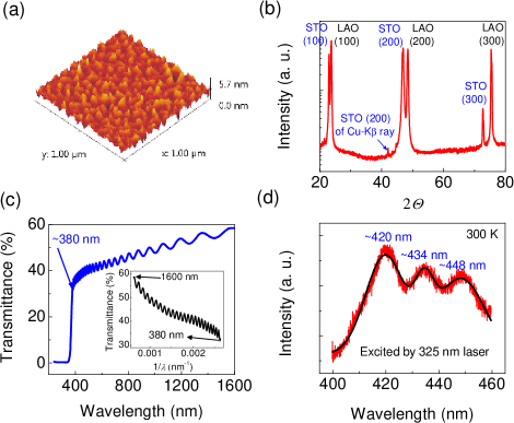
The 3D atomic force microscope image of the topography of the as-deposited STO film on the LAO substrate [Fig. 1(a)] shows the variation in the -dimension which is less than 6 nm. The root mean square value of the surface roughness in this 1 m 1 m area is only 0.541 nm, revealing a quite flat surface considering the film thickness of 2.6 m determined by surface profile measuring system. The x-ray diffraction (Cu-K ray) pattern of the STO film is shown in Fig. 1(b). The adjacent double diffraction peaks of the film and the substrate for each order indicate the typical characteristic of epitaxial growth. LAO is an excellent substrate to study oxygen deficient films because it is fairly difficult to create oxygen vacancies inside. Although it is a polar material, the bulk LAO will experience surface reconstruction and thus its surface would be nonpolar. This was con?rmed by our experiments, where STO layer-by-layer grown on fully LaO-terminated LAO was highly insulating, indicating no polar discontinuity at the interface.
The deposited STO film was reduced by annealing the sample at 950∘C and Torr vacuum for 1 hour. The transmittance spectrum [Fig. 1(c)] of the oxygen deficient STO film was measured using ultraviolet-visible (UV) spectroscopy from 240 to 1600 nm. The absorption edge is 380 nm, well corresponding to the band gap of STO. This suggests that after vacuum annealing the lattice structure of the STO film is still well standing. The spectrum displays an interference pattern with relatively high transmittance above 380 nm, which pertains to a scenario where the thick and highly smooth STO film serves as a Fabry-Perot interferometer. So the transmittance will show peaks when the wavelength of the normal incident optical wave meets the following condition:
| (1) |
where is the refractive index as a function of wavelength due to the strong dispersion [17], is the film thickness and is the order of the fringe. Equivalently, the transmittance will periodically oscillate with at a period of . To simply estimate the film thickness from the oscillations, take an intermediate refractive index 2.0516 [18], to keep as a constant. Thus if the transmittance data of the wavelength from 380 to 1600 nm are plotted versus as shown in the inset of Fig. 1(c), the average period of the oscillations in will be . The fitted average period is nm-1 and therefore the derived thickness is 2524 nm. The value is consistent with the directly measured one but slightly smaller since the intrinsic refractive index should be smaller than that of a usual STO film due to the oxygen vacancies [19].
The optical absorption of free electrons generated from oxygen vacancies is not seen in the UV spectroscopy, which typically leads to a decrease in transmittance especially in the long wavelength region and is likely buried by the strong interference here. However, the multiple photoluminescence (PL) emission peaks mostly from the oxygen vacancies [20] can be clearly seen [Fig. 1(d)]. The three PL peaks correspond to the energy intervals 2.95, 2.86 and 2.76 eV, respectively.
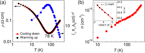
The transport properties of the vacuum-annealed STO film were measured by a Quantum Design PPMS machine. Aluminum wires were used through wire bonding for contacts. The temperature dependence of the resistivity measured by 10 A is shown on a logarithmic scale in Fig. 2(a). There is no observable difference between the cooling down and warming up curves. The curves reveal an obvious metal-insulator transition at K: at higher temperatures above 78 K, the resistivity is small and presents metallic behavior; nevertheless, the resistivity begins to increase with decreasing temperature dramatically from 78 K and reaches nearly six times the RT resistivity at 2 K. Figure 2(b) shows that the carrier density decreases by an order of magnitude when decreasing the temperature from 300 to 10 K.These are well the characteristics of a carrier freeze-out phenomenon [9,21]; the density of donors (oxygen vacancies here) is low such that the donor level is separated from the bottom of the conduction band. Hence once the temperature decreases to some extent, most of free electrons will shrink down to the lower donor level and get trapped.
The activation energy at high temperatures, fitted using
| (2) |
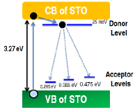
is 25 meV [inset of Fig. 2(b)], which is close to the RT thermal energy. Simply taking this value to characterize the energy interval between the donor level and the bottom of the conduction band, a band diagram of the oxygen deficient STO film can be obtained as depicted in Fig. 3 on the basis of the PL emission peaks [Fig. 1(d)]. The defect levels (close to the valence band) of STO are consistent with [20]. The resistivity ( cm) and carrier density ( cm-3) at RT of the STO film are respectively times smaller and 30 times larger than those of the bulk samples with the similar carrier freeze-out phenomenon [9]. These strongly suggest that the uniform area of the oxygen vacancies in a bulk STO is at most one-tenth of the whole single crystal thickness. So all the previous data of the resistivity and carrier density [6-11] related to the bulk STO should be re-considered carefully.
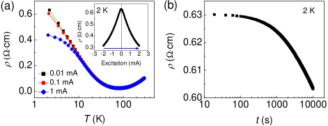
The corresponding carrier mobility from 300 to 10 K [Fig. 2(a)] is overall small and peaks around the phase transition temperature below which the mobility decreases with decreasing temperature due to the carrier freezing. At high temperatures the linear power law dependence of the mobility on temperature is more obvious. The frozen state can be re-excited by larger electric fields at low temperatures. As shown in Fig. 4(a), the resistivity decreases with increasing measuring current especially below 10 K. At 2 K, the resistivity obtained from measurement clearly displays a large negative electroresistance originated from the electrical excitation to trapped electrons, which can be defined as and reaches when the excitation current is 2 mA [inset of Fig. 4(a)]. Additionally, it was found that there is also a time dependence of the resistivity for the frozen state. As seen in Fig. 4(b), the resistivity at 2 K relaxes with the continuous measuring time, which suggests that the thermal effect is playing an important role during measurement. It can be understood by the ideas that the thermal conductivity of STO is very low [10] over the whole temperature range from 1.4 to 100 K and moreover after reducing there will be a significant decrease [22] due to the scattering of phonons from oxygen vacancies. Therefore the local temperature on the sample surface would increase as a result of the Joule heat accumulation, eventually yielding a decrease in resistivity under the low temperature frozen non-metallic state. However, the thermal effect at 2 K is much weaker than the electrical re-excitation.
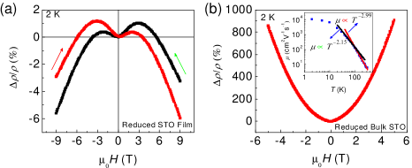
The 9 T magnetic field applied perpendicular to the STO film surface results in a negative MR although it is relatively small and can only be seen below 5 K in the curves. The MR curve of 2 K up to 9 T is shown in Fig. 5(a). It was found there was an asymmetry in the first curve obtained by scanning field from -9 to 9 T. To check whether the asymmetry was due to an improper measuring geometry, the sample was warmed up to RT and then cooled down to 2 K again to repeat the measurement but scanning field from 9 to -9 T. It was found there is always an asymmetry generated from an additional overall decrease in resistivity over the measuring time regardless of the scanning sequence of magnetic field; this indicates the asymmetry in the MR curves is from the thermal effect rather than the measurement geometry. Considering deducting the thermal effect, the shape of the MR curve at 2 K would be more close to a letter ’M’. The positive MR under small magnetic fields can be easily elucidated by the typical Lorentz scattering because the magnetic field is perpendicular to the current. The positive MR is very small because of the poor mobility of the charge carriers in the frozen state. However, there should still be another mechanism competing with the Lorentz scattering to account for the negative MR. Considering that the resistance at low temperatures is predominantly due to the trapping of carriers, so it seems plausible to imagine that the large magnetic field can somehow help to physically detrap the localized electrons from the trapping centers with the assistance of an excitation electric field through the Lorentz force. This could be more appropriate to the specific case here although a large number of mechanisms can result in a negative MR.On the other hand, oxygen vacancies in the TiO2 interface layer can also enhance the tendency for ferromagnetism considerably [23] similar to the Ti 3d electrons from interface charge transfer [4,24],which may also be possible for the negative MR seen here.
The bulk STO single crystal, vacuum-annealed together with the STO film, is metallic over the whole temperature range of K. The quadratic MR at 2 K [Fig. 5(b)] is quite large up to 900% at 5 T because of an extremely high mobility exceeding 10 000 cm2V-1s-1 [inset of Fig. 5(b)] and does not show any signature of a negative MR up to 5 T. This strengthens the idea that the negative MR of the oxygen deficient STO film is closely related to the carrier freezing state. Additionally, the bulk STO seems to be more conductive than the STO film since there is no carrier freeze-out in it. This evinces that the local concentration of oxygen vacancies in the bulk STO surface is larger than that in the STO film although they were reduced together, which strongly suggests that there is a sharp gradient in the concentration of oxygen vacancies in the bulk STO sample from the surface to inside. Thus all the electrical properties related phenomena in oxygen deficient bulk STO should be mostly just the local properties of the near surface area.
Interestingly, the behavior of the carrier freeze-out observed here is quite comparable to the spin glass behavior [25,26], for example, the carrier freezing transition, the relaxation of the frozen resistivity (although here is due to the thermal effect), and the suppression of the frozen state by the external fields. From this aspect, we can also coin this as ”charge glass” to more vividly represent its characteristics.
In summary, we argued the uniformity of oxygen vacancies in the bulk STO single crystals by studying the high quality STO single crystal film via various means. It was found the actual uniform thickness of the bulk STO is around several ten times smaller than the whole thickness and all the intriguing electrical phenomena of the oxygen deficient bulk STO could only be the local surface properties due to the obvious gradient in the concentrations of oxygen vacancies from surface to inside. Moreover, we investigated the MIT observed in the oxygen deficient STO film. The low temperature frozen state can be remarkably re-excited by the applied electric field. The thermal effect in oxygen deficient STO film during the electrical measurements is pronounced due to its poor thermal conductivity although the re-excitation of thermal effect to the low temperature frozen state is far less effective than the electric field. It was also found that large external magnetic fields can suppress the carrier freezing and generate negative MR. The possible mechanism proposed for that is the magnetic field can detrap the localized electrons under the frozen state through Lorentz force with the help of an electric excitation. The high similarity between the various behaviors of the carrier freeze-out and the spin glass state enables us to think the carrier freezing state as a kind of ”charge glass” state.
Acknowledgements.
We thank the National Research Foundation (NRF) Singapore under the Competitive Research Program (CRP) ’Tailoring Oxide Electronics by Atomic Control’ NRF2008NRF-CRP002-024, Natinoal Uinersity of Singapore (NUS) cross-faculty grant and FRC (ARF Grant No. R-144-000-278-112)for financial support.References
- (1) K. A. Müller and H. Burkard, Phys. Rev. B 19, 3593 (1979).
- (2) A. F. Santander-Syro et al., Nature 469, 189 (2011).
- (3) W. Meevasana et al., Nature Mater. 10, 114 (2011).
- (4) Ariando et al., Nature Commun. 2, 188 (2011).
- (5) K. van Benthem et al., J. Appl. Phys. 90, 6156 (2001).
- (6) J. F. Schooley, W. R. Hosler and M. L. Cohen, Phys. Rev. Lett. 12, 474 (1964).
- (7) J. F. Schooley et al., Phys. Rev. Lett. 14, 305 (1965).
- (8) H. P. R. Frederikse, W. R. Hosler, W. R. Thurber, J. Babiskin and P. G. Siebenmann, Phys, Rev. 158, 775 (1967).
- (9) O. N. Tufte and P. W. Chapman, Phys. Rev. 155, 796 (1967).
- (10) H. P. R. Frederikse, W. R. Thurber and W. R. Hosler, Phys. Rev. 134, A442 (1964).
- (11) C. S. Koonce, M. L. Cohen, J. F. Schooley, W. R. Hosler and E. R. Pfeiffer, Phys. Rev. 163, 380 (1967).
- (12) A. E. Paladino, L. G. Rubin and J. S. Waugh, J. Phys. Chem. Solids 26, 391(1965).
- (13) Ohtomo and H. Y. Hwang, 427, 423 (2004).
- (14) C. Herring, J. Appl. Phys. 31, 1939 (1960).
- (15) H. Fujisada, S. Kataoka and A. C. Beer, Phys. Rev. B 3, 3249 (1971).
- (16) M. Imada, A. Fujimori and Y. Tokura, Rev. Mod. Phys. 70, 1039 (1998).
- (17) M. Wölecke, V. Marrello and A. Onton, J. Appl. Phys. 48, 1748 (1977).
- (18) Y. Du et al., Appl. Phys. A: Mater. Sci. Process. 76, 1105 (2003).
- (19) A. Dejneka et al., Phys. Solid State 52, 2082 (2010).
- (20) D. Kan et al., Nat. Mater. 4, 816 (2005).
- (21) T. C. Harman, H. L. Goering and A. C. Beer, Phys. Rev. 104, 1562 (1956).
- (22) C. Yu et al., Appl. Phys. Lett. 92, 191944 (2008).
- (23) N. Pavlenko et al., arXiv:1105.1163v1.
- (24) A. Brinkman et al., Nature Mater. 6, 493 (2007).
- (25) K. Binder and A. P. Young, Rev. Mod. Phys. 58, 801 (1986).
- (26) M. D. Mukadam et al., J. Appl. Phys. 103, 123902 (2008).