Observation of the Kondo Effect in a Spin- Hole Quantum Dot
Abstract
We report the observation of Kondo physics in a spin- hole quantum dot. The dot is formed close to pinch-off in a hole quantum wire defined in an undoped AlGaAs/GaAs heterostructure. We clearly observe two distinctive hallmarks of quantum dot Kondo physics. First, the Zeeman spin-splitting of the zero-bias peak in the differential conductance is independent of gate voltage. Second, this splitting is twice as large as the splitting for the lowest one-dimensional subband. We show that the Zeeman splitting of the zero-bias peak is highly-anisotropic, and attribute this to the strong spin-orbit interaction for holes in GaAs.
pacs:
72.15.Qm, 73.63.-b, 75.70.TjThe observation of an unexpected minimum in the low temperature resistance of metals by de Haas in 1933 was ultimately explained thirty years later by Kondo as being due to interactions between a single magnetic impurity and the sea of conduction electrons in a metal deHaasPhysica33 ; KondoPTP64 . More recently there has been a resurgence of interest in the Kondo effect, following the discovery that the conductance of a few electron quantum dot in the Coulomb blockade regime is enhanced when the dot contains an odd number of electrons KouwenhovenPW01 ; GoldhaberNat98 ; CronenwettSci98 . There is a direct analogy with the Kondo effect in metals, with the localized electron in the quantum dot acting as a magnetic impurity that interacts with the two-dimensional sea of electrons in the source and drain reservoirs.
Studies of the Kondo effect in bulk systems have progressed since the 1960s, with the focus shifting towards manifestations of Kondo physics in the strongly correlated electron systems formed in cuprates and heavy-fermion metals StewartRMP01 . More precise control via improved electrostatic gate design has similarly allowed progress towards the study of more exotic manifestations of Kondo phenomena in quantum dots such as the integer-spin SasakiNat00 ; vanderWielPRL02 ; GrangerPRB05 , two-impurity JeongSci01 , and orbital Kondo effects Jarillo-HerreroNat05 . Thus far all quantum dot Kondo studies have involved electrons, and GaAs hole quantum dots present an interesting next step. Holes in GaAs originate from -like orbitals and behave as spin- particles due to strong spin-orbit coupling WinklerPRL00 . In two- and one-dimensional systems, the spin- nature of holes leads to remarkable, highly-anisotropic phenomena PapadakisPRL00 ; DanneauPRL06 ; RokhinsonPRL06 ; KlochanNJP09 ; ChenNJP10 not observed in electron systems, and new physics is expected for hole quantum dots also AndlauerPRB09 . Studies of Kondo physics in hole quantum dots may also provide useful connections to recent studies in bulk strongly correlated systems SuzukiPRB10 ; SlebarskiPRB10 .
Here we report the observation of the Kondo effect in a GaAs hole quantum dot. Due to the poor stability of conventional gate-defined modulation doped structures EnsslinNP06 it has not been possible to define hole quantum dots small enough for studies of Kondo physics GoldhaberNat98 . Instead, we follow the approach of Sfigakis et al. SfigakisPRL08 , where roughness in the walls of a wet-etched quantum wire led to formation of an incidental quantum dot exhibiting Kondo physics as the wire approached pinch-off. A key advantage to this approach is the ability to obtain an independent estimate of the effective Landé -factor . Using this we have fabricated a small hole quantum dot and conclusively demonstrate the “smoking gun” for Kondo physics MeirPRL93 – a splitting of the zero-bias peak in the differential conductance that opens as in response to an in-plane magnetic field and is independent of the gate voltage GoldhaberNat98 ; CronenwettSci98 . In contrast to electrons, we find that the field splitting of the zero-bias peak is highly anisotropic.
We used a heterostructure consisting of the following layers grown on a (100)-oriented substrate: m undoped GaAs, nm undoped AlGaAs barrier, nm undoped GaAs spacer and a nm GaAs cap degenerately doped with carbon for use as a metallic gate ClarkeJAP06 ; KlochanAPL06 . A (100) heterostructure was used to avoid the crystallographic asymmetries that plague (311)A heterostructures KlochanNJP09 ; ChenNJP10 . Ohmic contacts are made with AuBe alloy annealed at C for s. Our devices are remarkably stable, owing to population with holes electrostatically rather than by ionized modulation dopants ClarkeJAP06 ; KlochanAPL06 . A nm long by nm wide quantum wire aligned along the crystallographic direction is fabricated by electron beam lithography, as shown in the lower left inset to Fig. 1(a). The quantum wire is defined by shallow etching the doped cap to a depth nm to form three gates – a central top-gate negatively biased to to control the hole density and two side-gates positively biased to to control the electrostatic width of the wire KlochanAPL06 ; ChenNJP10 . The quantum dot forms as the wire approaches pinch-off, as discussed in the following paragraph. All data were obtained at V corresponding to a 2D hole density cm-2 and mobility cm2/Vs. We used standard lock-in techniques to measure the two terminal differential conductance with a variable dc source-drain bias added to a constant V ac excitation at Hz. A constant series resistance of k was subtracted from all measurements presented. The experiment was performed in a dilution refrigerator with a base temperature of mK, which featured an in-situ rotator that enabled the sample to be reoriented with respect to the applied magnetic field without the sample temperature exceeding mK YeohRSI10 .
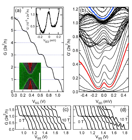
Figure 1(a) shows the linear conductance versus with the six quantized conductance plateaus confirming ballistic transport through the device. The quantum dot forms at due to a combination of microscopic deviations in confining potential due to etch roughness in the gates SfigakisPRL08 and self-consistent electrostatic effects YoonPRL07 . The presence of a bound-state in this system is revealed by the evolution of versus with increasing in-plane magnetic field aligned parallel [Fig. 1(c)] and perpendicular [Fig. 1(d)] to the wire at . In both cases, plateaus at and emerge, indicating the onset of spin-splitting PatelPRB91 , accompanied by sharp resonances signalling formation of a bound-state within the wire McEuenSurfSci90 ; LiangPRL98 ; SfigakisPRL08 ; KomijaniEPL10 . We will show later in Fig. 2(a) that this bound-state is not an impurity effect, as it is robust to gate-induced lateral shifting of the 1D channel GlazmanSST91 . Coupling of the magnetic field to orbital motion QuayNP10 may be responsible for differences in resonant structure between Figs. 1(c/d), as any random disorder potential should be constant given both orientations were measured during a single cooldown.
A study of the zero-bias peak (ZBP) in the differential conductance provides additional evidence for quantum dot formation. Figure 1(b) shows versus at a range of spanning , with two traces highlighted. Under a single particle picture, should depend quadratically on with a minimum at MartinMorenoJPCM92 , as observed for the blue trace at in Fig. 1(b). In contrast at , shows a pronounced peak at superimposed upon a parabolic background [red trace, Fig. 1(b)], known as the zero-bias peak. We observe the ZBP at conductances as low as , consistent with previous work SfigakisPRL08 ; SarkozyPRB09 ; RenPRB10 . This is demonstrated upper right inset to Fig. 1(a).
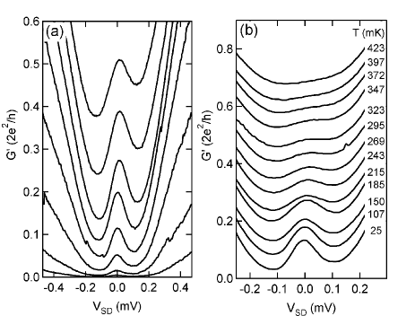
To demonstrate that the ZBP is robust and not due to random disorder ChenPRB09 , we have studied the ZBP as the wire is shifted laterally. We do this by repeating each measurement in Fig. 1(b) with a voltage offset of V added to side-gate 1 and subtracted from side-gate 2, such that the average bias is maintained to facilitate direct comparison. This results in a lateral shift of the wire by 60 nm GlazmanSST91 , and gives the data shown in Fig. 2(a) For traces below there is almost no change in the ZBP compared to the data from the unshifted channel in Fig. 1(b), confirming that the ZBP is not disorder-induced. Equivalent data was obtained when we shifted the channel in the opposite direction (not shown). To further check the consistency of our ZBP with the known Kondo physics of electron quantum dots, in Fig. 2(b) we show the evolution of the red trace from Fig. 1(b) with temperature . The peak widens and decreases in amplitude with increasing , consistent with previous studies CronenwettSci98 .
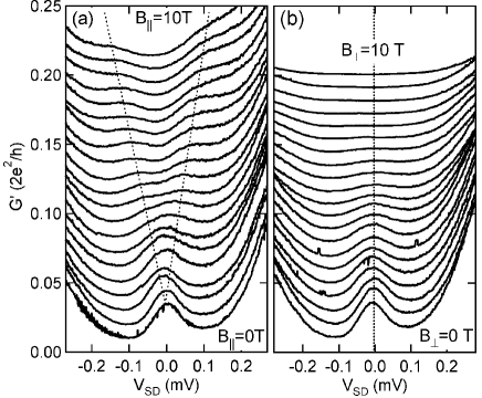
We now focus on the magnetic field dependence of the zero-bias peak looking for: a) the anisotropy characteristic of spin- holes, and b) the distinctive peak splitting of Kondo physics. We begin by examining the evolution of the ZBP with in Fig. 3(a). Initially no splitting is resolved and the only change is a widening of the zero-bias peak. However, at T two peaks become resolved, and these separate in as is increased further. The behavior is very different with an in-plane field applied perpendicular to the wire [Fig. 3(b)]. Here the peak shows no splitting even at the highest field T; instead the peak is gradually reduced in amplitude and ultimately suppressed entirely. This anisotropic behavior matches the underlying anisotropy of the 1D wire ChenNJP10 in which the dot resides. We return to this anisotropy in the final discussion, and now continue with quantitative analysis of the peak splitting with .
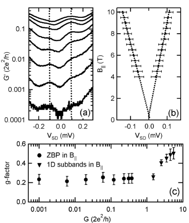
As pointed out by Cronenwett et al. in Ref. CronenwettSci98 , the most distinct sign of the quantum dot Kondo effect is a gate voltage independent ZBP split by . Figure 4(a) shows versus at various at T. The two vertical dotted lines in Fig. 4(a) pass through the field-split zero-bias peaks over more than three orders of magnitude in conductance, demonstrating the gate voltage independence of the peak splitting. Turning to the splitting as a function of field, in Fig. 4(b) we plot the peak location in for the traces in Fig. 3(a) where two peaks can be clearly resolved against . The peak locations are determined by eye and the error bars are estimated knowing that the ZBP sits on a parabolic background with a slight linear asymmetry from the way that is applied in the measurement circuit. The ZBP clearly splits linearly with in Fig. 4(b), giving if we assume a splitting . The data will justify this assumption below. We repeated this analysis at eight different conductances between and giving the solid circles plotted in Fig. 4(c). The error bars are obtained from a regression analysis of linear fits such as that in Fig. 4(b). The values obtained are constant over three orders of magnitude in , in agreement with Fig. 4(a), and give an average .
A natural question is: How do we know that the peak splitting is given by rather than , which would increase the extracted from the data by a factor of two? The key advantage of our device is that we can use 1D subband spectroscopy PatelPRB91 to independently measure in the limit where approaches from above. This allows us to corroborate our measurement of . We measure for the first five 1D subbands using the method in Ref. ChenNJP10 and the usual Zeeman expression for 1D subbands PatelPRB91 . The resulting values, plotted as solid triangles in Fig. 4(c), decrease linearly as approaches . This linear decrease is distinctive of holes in (100) heterostructures ChenNJP10 . However, the most significant aspect is that the obtained for the lowest 1D subband assuming the 1D splitting goes as is in excellent agreement with obtained assuming the ZBP splitting goes as . This is “smoking gun” evidence confirming our observation of Kondo physics in a hole quantum dot MeirPRL93 ; GoldhaberNat98 ; CronenwettSci98 .
We conclude by discussing some key implications of our findings. The magnitude and anisotropy of closely matches that of for the lowest 1D subband. This suggests that is set by the prevailing of the environment hosting the dot. It agrees with quantum dots CronenwettSci98 , where the splitting of the ZBP gives the same as bulk GaAs, and with carbon nanotubes NygardNat00 . The fact that a spin- system produces no radical change in the observed Kondo physics is interesting, as it implies that the process only relies on the presence of a doubly-degenerate quantum dot level to mediate transport between the reservoirs, and not its precise nature/spin. This is in accordance with recent studies of more exotic manifestations of Kondo physics in quantum dots SasakiNat00 ; vanderWielPRL02 ; GrangerPRB05 ; JeongSci01 ; Jarillo-HerreroNat05 . However, a spin- system may ultimately present more subtle changes, for example, confinement-induced mixing ZulickePSSC06 between heavy-hole and light-hole subbands (i.e., states with total angular momentum quantum numbers and respectively) may alter the relevant scales in the problem. Further studies in this direction would be useful, including both theoretical work and measurements from improved device geometries. Finally, we comment briefly on the bearing of our results on studies of the anomaly ThomasPRL96 in 1D systems. Although we observe a plateau-like feature near in our device (see Figs. 1(a,c,d)), the presence of the resonant structure in the linear conductance precludes any direct and definitive link between the anomaly and the behavior we observe for our zero-bias peak. We emphasize that the gate-voltage independent Zeeman splitting of our ZBP points conclusively to the quantum dot Kondo effect, in contrast with the gate-voltage dependent zero-bias anomaly (ZBA) splitting observed in undoped quantum wires by Sarkozy et al. SarkozyPRB09 . The characteristics of our zero-bias peak are very different to those of the ZBA in quantum wires. The two effects clearly have a different origin, which agrees with the suggestion by Sarkozy et al. SarkozyPRB09 that the ZBA is a fundamental property of quantum wires, and suggests that it may involve processes beyond Kondo physics alone.
This work was funded by the Australian Research Council (Grant Nos. DP0772946, DP0986730, FT0990285). We thank U. Zülicke for helpful discussions, L.A. Yeoh and A. Srinivasan for development of the low temperature rotator, and J. Cochrane for technical support.
References
- (1) W.J. de Haas, J. de Boer, and G.J. van den Berg, Physica 1, 1115 (1933).
- (2) J. Kondo, Prog. Theor. Phys. 32, 37 (1964).
- (3) L.P. Kouwenhoven and L.I. Glazman, Physics World 14(1), 33 (2001).
- (4) D. Goldhaber-Gordon et al., Nature 391, 156 (1998).
- (5) S.M. Cronenwett, T.H. Oosterkamp and L.P. Kouwenhoven, Science 281, 540 (1998).
- (6) G.R. Stewart, Rev. Mod. Phys. 73, 797 (2001).
- (7) S. Sasaki et al., Nature 405, 764 (2000).
- (8) W.G. van der Wiel et al., Phys. Rev. Lett. 88, 126803 (2002).
- (9) G. Granger et al., Phys. Rev. B 72, 165309 (2005).
- (10) H. Jeong, A.M. Chang and M.R. Melloch, Science 293, 2221 (2001).
- (11) P. Jarillo-Herrero et al., Nature 434, 484 (2005).
- (12) R. Winkler et al., Phys. Rev. Lett. 85, 4574 (2000).
- (13) S.J. Papadakis et al., Phys. Rev. Lett. 84, 5592 (2000).
- (14) R. Danneau et al., Phys. Rev. Lett. 97, 026403 (2006).
- (15) L.P. Rokhinson, L.N. Pfeiffer, and K.W. West, Phys. Rev. Lett. 96, 156602 (2006).
- (16) O. Klochan et al., New J. Phys. 11, 043018 (2009).
- (17) J.C.H. Chen et al., New J. Phys. 12, 033043 (2010).
- (18) T. Andlauer and P. Vogl, Phys. Rev. B 79, 045307 (2009).
- (19) K. Suzuki et al., Phys. Rev. B 82, 054519 (2010).
- (20) A. Ślebarski et al., Phys. Rev. B 82, 235106 (2010).
- (21) K. Ensslin, Nat. Phys. 2, 587 (2006).
- (22) F. Sfigakis et al., Phys. Rev. Lett. 100, 026807 (2008).
- (23) Y. Meir, N.S. Wingreen, and P.A. Lee, Phys. Rev. Lett. 70, 2601 (1993).
- (24) W.R. Clarke et al., J. Appl. Phys. 99, 023707 (2006).
- (25) O. Klochan et al., Appl. Phys. Lett. 89, 092105 (2006).
- (26) L.A. Yeoh et al., Rev. Sci. Instrum. 81, 113905 (2010).
- (27) Y. Yoon et al., Phys. Rev. Lett. 99, 136805 (2007).
- (28) N.K. Patel et al., Phys. Rev. B 44, 13549 (1991).
- (29) P.L. McEuen et al., Surf. Sci. 229, 312 (1990).
- (30) C.-T. Liang et al., Phys. Rev. Lett. 81, 3507 (1998).
- (31) Y. Komijani et al., Europhys. Lett. 91, 67010 (2010).
- (32) L.I. Glazman and I.A. Larkin, Semicond. Sci. Technol. 6, 32 (1991).
- (33) C.H.L. Quay et al., Nature Physics 6, 336 (2010).
- (34) L. Martín-Moreno et al., J. Phys.: Condens. Matter 4, 1323 (1992).
- (35) S. Sarkozy et al., Phys. Rev. B 79, 161307 (2009).
- (36) Y. Ren et al., Phys. Rev. B 82, 045313 (2010).
- (37) T.-M. Chen et al., Phys. Rev. B 79, 153303 (2009).
- (38) J. Nygård et al., Nature 408, 343 (2000).
- (39) U. Zülicke, Phys. Stat. Sol. (c) 3, 4354 (2006)
- (40) K.J. Thomas et al., Phys. Rev. Lett. 77, 135 (1996).