Inhomogenous electronic structure, transport gap, and percolation threshold in disordered bilayer graphene
Abstract
The inhomogenous real-space electronic structure of gapless and gapped disordered bilayer graphene is calculated in the presence of quenched charge impurities. For gapped bilayer graphene we find that for current experimental conditions the amplitude of the fluctuations of the screened disorder potential is of the order of (or often larger than) the intrinsic gap, , induced by the application of a perpendicular electric field. We calculate the crossover chemical potential, , separating the insulating regime from a percolative regime in which less than half of the area of the bilayer graphene sample is insulating. We find that most of the current experiments are in the percolative regime with . The huge suppression of compared with provides a possible explanation for the large difference between the theoretical band gap and the experimentally extracted transport gap.
One of the unique properties of single layer graphene, SLG, Novoselov et al. (2004) is its high room-temperature electronic mobility Das Sarma et al. (2010). This fact makes graphene of great interest for possible technological applications. However, the lack of a band gap implies that in SLG the current can never be turned off completely (i.e. SLG has a very low on/off ratio in the engineering jargon) and therefore limits the possible use of SLG in transistor or switching applications. The mobility of bilayer graphene, BLG, is normally lower than the mobility of SLG Morozov et al. (2008); Xiao et al. (2010); Hwang et al. (2009), but it can be very high when Boron-Nitride is used as a substrate Dean et al. (2010); Das Sarma and Hwang (2011). Most importantly, by applying a perpendicular electric field Castro et al. (2007); Min et al. (2007); Zhang et al. (2009a); Oostinga et al. (2008); Taychatanapat and Jarillo-Herrero (2010); Zou and Zhu (2010); Yan and Fuhrer (2010), a gap of up to 250 meV can be opened in the band structure of BLG which should strongly enhance the on/off switching ratio. The strictly 2D nature of the carriers, the high room-temperature mobility, and the ability to open and tune , make BLG an extremely interesting material both from a fundamental and a technological point of view. In recent BLG experiments Oostinga et al. (2008); Taychatanapat and Jarillo-Herrero (2010); Zou and Zhu (2010) the activated transport gap has been found to be orders of magnitude smaller than . This finding has been explained assuming that transport is in the variable range hopping regime, VRH, Oostinga et al. (2008); Taychatanapat and Jarillo-Herrero (2010); Zou and Zhu (2010), or that edge modes might contribute significantly to transport Li et al. (2011). Resonant scattering centers have been proposed as the dominant source of disorder Wehling et al. (2010) in both SLG and BLG. In gapped BLG the resonant scatterers would induce localized states that would then mediate transport via VRH. However scanning tunneling microscopy experiments have so far not shown direct evidence of resonant states suggesting that their density might be quite low, in addition no sign of localization is ever observed in ungapped BLG even in the presence of strong disorder. On the other hand, the edge modes can significantly contribute only if scattering between counter-propagating edge modes is suppressed. Because the BLG band structure is characterized by two equivalent valleys with opposite chirality, even small quantities of short-range defects can mix the fermionic states of the two valleys and greatly suppress the contribution of the edge modes to transport Yan and Fuhrer (2010). These facts motivated us to look for a possible alternative explanation to the smallness of the experimental BLG transport gap compared to based on the disorder-induced massive breakdown of momentum conservation.
Our model is based on the assumption that charge impurities are the dominant source of disorder in exfoliated BLG samples. There is ample evidence Das Sarma et al. (2010) that this assumption is at least consistent with most of the transport experiments on gapless SLG and BLG although other scattering sources might play an important role Wehling et al. (2010); Katsnelson and Geim (2008). In particular we assume the charge impurities to be located at a typical distance nm from the graphenic layer and to be uncorrelated. In reality some degree of correlation is expected but it does not affect qualitatively our results. In the presence of charge impurities the carrier density becomes strongly inhomogenous. The importance of density inhomogeneities for the understanding of the physics, especially transport, of 2D electronic systems has been appreciated in the context of the Quantum Hall, QH, effect disorderQH and of standard 2D electron gases, 2DEGs, in which the gap between the hole-band and the electron-band is much larger than the disorder strength disorderLargeGap . The case of gapped BLG is different from these cases because no magnetic field is present and so the dispersion is not broken-up in Landau Levels and yet the band-gap is small compared to the strength of the disorder potential. We emphasize, moreover, that the transport phase diagram, which is the main topic of our work , has never before been addressed in the literature for any system. In BLG we therefore have the unique condition of a small band gap between non-degenerate valence and conduction bands. The most striking and counterintuitive consequence of this fact is that, as we show below, in gapped BLG an increase of the disorder strength can drive the system from being an insulator to be a bad metal when the chemical potential, , is within the gap. This behavior is the opposite of what happens in a standard 2DEG in which an increase of the disorder strength drives the system to an insulating state. By showing that the disorder can effectively drive BLG to a metal state even when is finite and is well within the gap, our work provides a compelling possible explanation for the large discrepancy between of gapped BLG and the gap extracted from transport measurements. We define an effective real-space gap, , that determines the transport properties and show that for disorder strengths typical in current experiments it can be zero even for as large as 150 meV. Although our specific calculations are carried out for gapped BLG systems, the general idea developed here, namely a spatially fluctuating local band gap in the presence of charged impurity disorder induced inhomogeneity, should apply to other systems, and we believe that the same idea could explain the experimental finding nanoribbons of rather small transport band gaps in graphene nanoribbon experiments where percolation effects are known to be important.
Our main goal is to find a qualitative explanation for the smallness of the transport gap compared to for the situation when charge impurities are the dominant source of disorder. To calculate the electronic structure in the presence of the disorder potential due to charge impurities we use the Thomas-Fermi theory, TFT. For SLG the TFT results Rossi and Das Sarma (2008) compare well with density functional theory, DFT, results Polini et al. (2008) and experiments Martin et al. (2008); Zhang et al. (2009b); Deshpande et al. (2009) as long as the impurity density is not too low () Brey and Fertig (2009). These results suggest that TFT might give reasonable results also for disordered BLG. TFT is valid when the density profile, , satisfies the inequality , with the Fermi wavevector. As shown below the density varies on length scales of the order of 10-20 nm whereas in the metallic regions , so that the inequality is only marginally satisfied. A complete quantitative validation of the TFT results can only be achieved by comparison to DFT results that however are not yet available for disordered BLG. On the other hand due to the computational cost DFT cannot be used to calculate disorder averaged quantities that are needed to extract the transport properties. TFT is therefore the only approach that can be used to address the issue of transport in BLG in the presence of long range disorder and, given that our goal is the qualitative understanding of the large difference between transport gap and , is also adequate. Moreover, the strong dependence of the transport gap on the details of the experiments (like the temperature range) makes a quantitative comparison of theory and experiments almost impossible. For this reason, and given the limited quantitative accuracy of TFT, for the band structure of BLG we use the simple model of 2 parabolic bands with effective mass . The simplicity of this model allows us to identify the few parameters that affect the qualitative features of the results and makes our findings relevant also to standard parabolic 2DEGs.
The TFT energy functional is given by:
| (1) |
where the static background dielectric constant, and the bare disorder potential. The first term is the kinetic energy, the second the Hartree part of the Coulomb interaction, and the third is the contribution due to the disorder potential. Assuming for the substrate, as appropriate for graphene on , in the remainder we set , average of the dielectric constant of vacuum and substrate. By differentiating with respect to we find:
| (2) |
where we have introduced the screening length nm.
At the energy minimum, . For the gapless case this equation can be solved analytically in momentum space to find
| (3) |
Let be the screened disorder potential. Using Eq. (3) we find:
| (4) |
We have , where are random numbers with Gaussian distribution such that and , where the angle brackets denote average over disorder realizations. Using Eq. (3), (4) and the statistical properties of , for the variance of the density, , we find
| (5) |
with , a dimensionless function (here is the incomplete gamma function). For small , (where is the Euler constant), whereas for . For the root mean square of the density, , and screened disorder potential, , we then have:
| (6) |
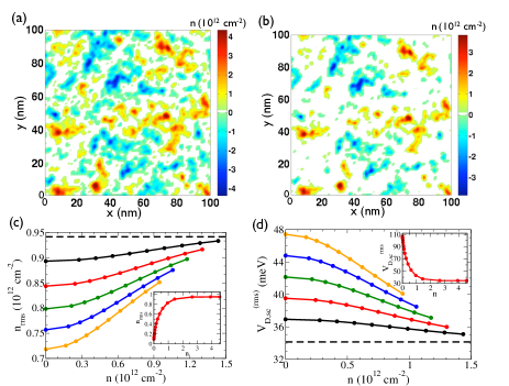
In the presence of a band gap the equation becomes nonlinear and an analytic expression for is not readily obtainable. We have solved the problem numerically for nm samples, with 1 nm spatial discretization, considering several (1000 or more) disorder realizations to then calculate the disorder averaged quantities. In Fig. 1 (a) and (b) we show our calculated carrier density landscapes for single disorder realizations for two values of , both with the same and fixed at the charge neutrality point, CNP. In the absence of disorder both situations in Fig. 1 (a) and (b) will manifest zero carrier density throughout with a pure intrinsic band gap at all spatial points (i.e. both sets of plots will be completely ’white’ in color since we are explicitly at T=0 with no thermal inter-band excitations). Fig. 1 (c) and (d) show the dependence of and , respectively, on the doping for values of the gap between 12 and 55 meV. is suppressed close to the CNP, due to the large area covered by insulating regions () whereas is higher close to the CNP due to the lack of screening. The results of Fig. 1 (c) and (d) are well fitted by the scalings , , with , and and expressed in units of and meV respectively.
The analysis of the disorder averaged results obtained from the TFT can be used to qualitatively understand the electronic transport in the highly inhomogeneous density landscape of gapped BLG. Let be the disorder averaged fraction of the area occupied by the insulating regions (white in Figs. 1 (a) and (b)). The color plots in Fig. 2 (a)-(c) show the dependence of on and the doping for three different values of . At high dopings and low disorder is fairly small. As decreases some hole puddles and insulating regions start appearing. The black line identifies the contour for which . Below the black line and we are in the strongly inhomogenous regime. The white line identifies the contour for which the area fraction occupied by electron puddles is equal to 50%. Below this line more than half of the sample area is occupied by hole puddles and insulating regions. Finally, the red line shows the contour for which is . Below this line more than half of the sample is covered by insulating regions. The counterintuitive result is that close to the CNP becomes smaller as increases with fixed. This is a consequence of the fact that as increases, the disorder becomes strong enough to bring the Fermi level inside the conduction or the valence band. Using the contour lines overlaid on the color-plot for we can qualitatively identify different semiclassical transport regimes. Regime I: Weak disorder where . The system is a good metal with an almost uniform density landscape. Regime II: Strong disorder . In this regime the density landscape breaks up in puddles and insulating regions. Because the area fraction covered by electrons is larger than 1/2 the system behaves like a metal via percolation through the electron puddles. Regime III: Weak-moderate disorder, , . Most of the sample area is insulating and the system is an insulator. Regime IV: In this regime the disorder is so strong, , that, despite the finite gap, is less than 50% but neither the electron puddles, nor the hole puddles alone cover more than 50% of the total area. The system should behave as a bad metal with the conductance determined by tunneling events across few narrow insulating regions separating the electron-hole puddles similar to transport at the CNP in gapless BLG Hwang and Das Sarma (2010) and SLG Rossi et al. (2009). It is obvious, looking at the color plots in Fig. 2(a)-(c) that at lower (higher) values of (disorder) the apparent transport gap will be strongly suppressed and in fact will be vanishingly small. We believe that this is the current physical situation in existing BLG systems.
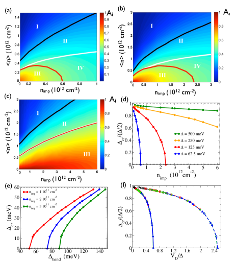
To identify the transport regime is useful to introduce the critical value of chemical potential, , for which =50%. For ( the system is expected to behave as bad metal (an insulator). For , is almost independent of the disorder strength. For small gaps, , depends strongly on the disorder strength, and . This is shown in Fig. 2 (d) in which the calculated as a function of is shown for four different values of . For fixed , decreases as increases. We see that for meV, for impurity densities of the order of the ones estimated in current experiments on exfoliated BLG (), can be orders of magnitude smaller than . Fig. 2 (e) shows as a function of for different values of . We see that for meV already for . In the presence of spatial correlations among impurities the density inhomogeneities are expected to be reduced and therefore the value of for which would increase. Finally Fig. 2 (f) shows the scaling of on the strength of the disorder potential, . The points connected by solid (dashed) lines show the dependence of with respect to (), with the rms of the bare disorder potential. In both cases, by normalizing both and with the band-gap, we find that the results obtained for different values of collapse on a single curve that does not depend on and away from scales approximately as , with for , and for .
In summary, using a simple 2-bands model and TFT, we have characterized the density inhomogeneities in gapless and gapped BLG. For gapless BLG we have found analytic expressions for and as a function of the experimental parameters and shown that they do not depend on the doping and scale like . For gapped BLG () is reduced (enhanced) with respect to the gapless case, in particular in the vicinity of the CNP. By calculating the disorder averaged fraction of the sample area, , covered by insulating regions we have qualitatively identified four different transport regimes. We have shown that most of the current experiments are expected to be in a regime, regime IV, in which the disorder is strong enough to reduce below 50% even at zero doping. In this regime, gapped BLG is expected to behave like a bad metal in which transport is dominated by hopping processes between electron and hole puddles that cover most of the sample. The value of the chemical potential for which identifies the crossover between the insulating regime and regime IV. We have shown how depends on the impurity density , the strength of the screened disorder potential, and the theoretical band gap . We believe the reduction of as a function of is the qualitative resolution of the contradiction between and the transport gap. A clear prediction of our theory is that in cleaner BLG (e.g. on boron nitride substrates) there should be close agreement between the transport gap and . We also predict agreement between and the transport gap for very large values of .
This work is supported by US-ONR and NRI-SWAN. E.R. acknowledges support from the Jeffress Memorial Trust, Grant No. J-1033. Computations were carried out on the University of Maryland High Performance Computing Cluster (HPCC) and the SciClone Cluster at the College of William and Mary.
References
- (1)
- Novoselov et al. (2004) K. S. Novoselov et al., Science 306, 666 (2004).
- Das Sarma et al. (2010) S. Das Sarma et al., Rev. Mod. Phys. 83, 407, (2011).
- Morozov et al. (2008) S. V. Morozov et al., Phys. Rev. Lett. 100, 016602 (2008).
- Xiao et al. (2010) S. Xiao et al., Phys. Rev. B 82, 041406 (2010).
- Hwang et al. (2009) E. H. Hwang et al., Phys. Rev. B 80, 235415 (2009).
- Dean et al. (2010) C. R. Dean et al., et al., Nature Nanotech. 5, 722 (2010).
- Das Sarma and Hwang (2011) S. Das Sarma and E. H. Hwang, Phys. Rev. B 83, 121405(R) (2011).
- Castro et al. (2007) E. V. Castro et al., Phys. Rev. Lett. 99, 216802 (2007).
- Min et al. (2007) H. Min et al., Phys. Rev. B 75, 155115 (2007).
- Zhang et al. (2009a) Y. B. Zhang et al., Nature 459, 820 (2009a).
- Oostinga et al. (2008) J. Oostinga et al., Nature Materials 7, 151 (2007).
- Taychatanapat and Jarillo-Herrero (2010) T. Taychatanapat and P. Jarillo-Herrero, Phys. Rev. Lett. 105, 166601 (2010).
- Zou and Zhu (2010) K. Zou and J. Zhu, Phys. Rev. B 82, 081407 (2010).
- Yan and Fuhrer (2010) J. Yan and M. S. Fuhrer, Nano Letters 10, 4521 (2010).
- Li et al. (2011) J. Li et al., Nat. Phys. 7, 38 (2011).
- Wehling et al. (2010) T. O. Wehling et al., Phys. Rev. Lett. 105, 056802 (2010), A. Ferreira et al., Phys. Rev. B 83, 165402 (2011).
- Katsnelson and Geim (2008) M. I. Katsnelson and A. K. Geim, Phil. Trans. R. Soc. A 366, 195 (2008). F. Guinea, Journ. Low Temp. Phys. 153, 359 (2008).
- (19) J. T. Chalker and P. D. Coddington, J. Phys. C-solid State Phys. 21, 2665 (1988); A. L. Efros, Phys. Rev. B 47, 2233 (1993); E. Shimshoni et al., Phys. Rev. Lett. 80, 3352 (1998);
- (20) E. Arnold, Surface Science 58, 60 (1976); A. L. Efros, Solid State Commun. 70, 253 (1989); Y. Meir, Phys. Rev. Lett. 83, 3506 (1999); S. Ilani et al., Science 292, 1354 (2001). J. Shi and X. C. Xie, Phys. Rev. Lett. 88, 086401 (2002); S. Das Sarma et al. Phys. Rev. Lett. 94, 136401 (2005); G. Allison et al., Phys. Rev. Lett. 96, 216407 (2006); M. J. Manfra et al., Phys. Rev. Lett. 99, 236402 (2007).
- (21) M. Han et al., Phys. Rev. Lett. 98, 206805 (2007) and 104, 056801 (2010), S. Adam et al. , Phys. Rev. Lett. 101, 046404 (2008), P. Gallagher, K. Todd, and D. Goldhaber-Gordon, Phys. Rev. B 81, 115409 (2010).
- Rossi and Das Sarma (2008) E. Rossi and S. Das Sarma, Phys. Rev. Lett. 101, 166803 (2008).
- Polini et al. (2008) M. Polini et al., Phys. Rev. B 78, 115426 (2008).
- Martin et al. (2008) J. Martin et al., Nature Physics 4, 144 (2008).
- Zhang et al. (2009b) Y. Zhang et al., Nature Physics 5, 722 (2009b).
- Deshpande et al. (2009) A. Deshpande et al., Phys. Rev. B 79, 205411 (2009).
- Brey and Fertig (2009) L. Brey and H. A. Fertig, Phys. Rev. B 80, 035406 (2009).
- Hwang and Das Sarma (2010) S. Das Sarma et al., Phys. Rev. B, 81, 161407 (2010), E. H. Hwang and S. Das Sarma, Phys. Rev. B 82, 081409 (2010).
- Rossi et al. (2009) E. Rossi et al., Phys. Rev. B 79, 245423 (2009).
- (30) Even for large electric fields in BLG saturates to meV. Results for meV are shown to illustrate qualitatively the situation typical in standard parabolic 2DEGs such as the ones created in GaAs and Si quantum wells.