Tunable graphene bandgaps from superstrate mediated interactions.
Abstract
A theory is presented for the strong enhancement of graphene-on-substrate bandgaps by attractive interactions mediated through phonons in a polarizable superstrate. It is demonstrated that gaps of up to 1eV can be formed for experimentally achievable values of electron-phonon coupling and phonon frequency. Gap enhancements range between 1 and 4, indicating possible benefits to graphene electronics through greater bandgap control for digital applications, lasers, LEDs and photovoltaics through the relatively simple application of polarizable materials such as SiO2 and Si3N4.
pacs:
73.22.PrI Introduction
A key goal for graphene research is the development of applications which require substantial bandgaps, such as digital transistors. Graphene monolayers have zero band gap, but small gaps have been observed when graphene is placed on substrates such as SiC (250meV) Zhou et al. (2007), gold on ruthenium (200meV) Enderlein et al. (2010) and predicted for graphene on boron nitride (100meV) Giovannetti et al. (2007). A technique for enhancing these gaps up to the 1eV order of magnitude seen in silicon is crucial to the development of digital electronics. Moreover, the ability to make spatially dependent changes to the gap of a semiconducting material should open a route to new electronic devices and applications, and the availability of strongly tunable gaps is important to the development of laser diodes, LEDs, photovoltaics, heterojunctions and photodetectors.
Here, I investigate gap enhancement effects due to interactions mediated through superstrates placed on graphene systems where a gap has been opened with a modulated potential. For example, sublattice symmetry breaking has been suggested for the gap opening mechanism for the graphene on ruthenium system Enderlein et al. (2010). The specific aim is to establish if the small gap size of e.g. graphene on ruthenium can be increased using attractive electron-phonon coupling to vibrations in a strongly polarizable superstrate. In low dimensional materials, strong effective electron-electron interactions can be induced via interaction between electrons confined to a plane and phonons in a neighboring layer which is polarizable Alexandrov and Kornilovitch (2002). In the context of carbon systems, experiment has shown that electron-phonon interactions between carbon nanotubes and SiO2 substrates have strong effects on transport properties Steiner et al. (2009) and theory has shown that similar interactions account for the transport properties of graphene on polarizable substrates Fratini and Guinea (2008).
Besides graphene on substrates, several alternative options have been put forward to generate gaps in graphene. McCann and Falko McCann and Fal’ko (2006); McCann et al. (2007) proposed that bilayer graphene develops a gap when it is gated with an electic field, and the bilayer graphene gap has been observed experimentally by Ohta et al. using ARPES Ohta et al. (2006) and by Zhang et al. using infrared spectroscopy Zhang et al. (2009).
Electron confinement in quasi-1D structures has also been put forward as a solution to the generation of bandgaps. Graphene nanoribbons with certain edge orientations were theoretically hypothesised some time ago to posess gaps Fujita et al. (1996); Nakada et al. (1996) and it has been shown using ab-initio calculations that reduction of the nanoribbon width can lead to substantial gap sizes due to electron confinement, although for gap sizes of the order of an electronvolt, very narrow nanoribbons with widths of the order of 10 Å are required. Increase in nanoribbon gaps up to around meV due to electron confinement has been measured by Han et al. Han et al. (2007) although the width variation of the ribbons is large. Recent developments have allowed for the manufacture of high quality nanoribbons by unzipping of nanotubes Kosynkin et al. (2009), and theoretical predictions have been confirmed experimentally, with a measured gap of meV for an (8,1) nanoribbon Tao et al. (2011).
A more extreme solution involves changing the chemistry of graphene monolayers. The generation of large band gaps in graphene on the order of several eV has been hypothesized for chemical modification with hydrogen (graphane) Sofo et al. (2007); Boukhvalov et al. (2008) and fluorine (fluorographene) Charlier et al. (1993). While forms of graphane Elias et al. (2009) and fluorographene Cheng et al. (2010) have been manufactured, and hints of bandgaps have been found, there is currently no consensus on the size of the bandgap, as it is difficult to obtain even coverage of the hydrogen or fluorine. Also, it is likely that the wide bandgaps are too large for many digital applications. Finally, I briefly mention that graphene on some substrates forms Moiré patterns, which also lead to a modified electronic structure MacDonald and Bistritzer (2011).
This paper is organized as follows: a model for graphene sandwiched between a dielectric superstrate and a gap-opening substrate is introduced in Sec. II. In Sec. III results from Hartree–Fock theory in the high phonon frequency limit are presented. Perturbation theory and results for low phonon frequency are presented in Sec. IV. A summary and outlook can be found in Sec. V.
II Model
A model Hamiltonian for the electronic properties of graphene on a substrate modified by the presence of a superstrate should have at least three components. The first is a mechanism for electrons to move through the material. The second is an electron-phonon interaction and the third a static potential to describe symmetry breaking between graphene sub-lattices by the substrate. The presence of superstrates also opens the possibility of long-range electron-phonon interactions. As such, a model Hamiltonian for graphene on a substrate has the form,
| (1) | |||||
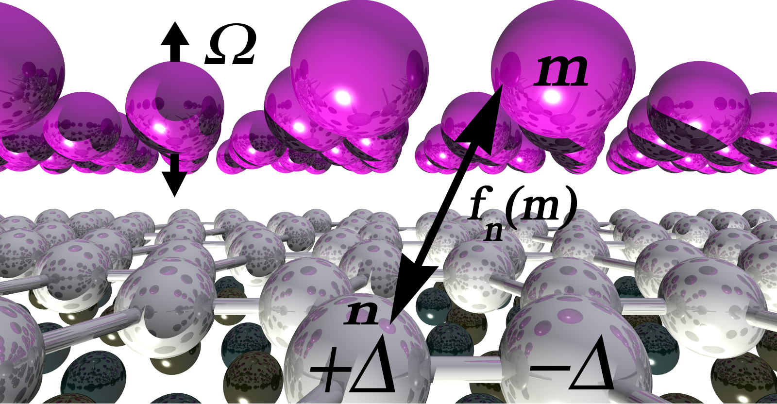
The interactions between electrons in a graphene monolayer and polarizable ions in the superstrate are shown schematically in Fig. 1. The first term in the Hamiltonian describes the kinetic energy of tight binding electrons hopping in the graphene monolayer with amplitude , written in momentum space as , where and are the nearest neighbor vectors from graphene A to B sites, , , . Electrons are created on graphene A sites with the operator and B sites with and the vectors are to atoms in the plane.
The next term in the Hamiltonian describes the electron-phonon interaction, which has the momentum space form . Phonons are created in the superstrate above A sites with and above the B sublattice with , so the displacement for site A. The interaction strength has the classic Fröhlich form ( is a coupling constant). The effective phonon-mediated interaction between electrons can be characterised by the function . A complication of this Hamiltonian is that a basis of two atoms is needed to represent the honeycomb lattice, which is the reason for two interactions; and . For local electron-phonon coupling, vanishes and becomes momentum independent. For simplicity, I study this simplified version of the electron-phonon Hamiltonian Covaci and Berciu (2008), i.e the effective interaction is approximated as a Holstein model which has local interaction, . The third term represents the energy of phonons with frequency , where is the number operator for phonons. It is appropriate to mention the effect of the electron-phonon interaction on suspended graphene, which simply leads to renormalizations of phonon and electron modes Neto et al. (2009); Covaci and Berciu (2008).
The Fröhlich form for the electron-phonon interaction has been demonstrated experimentally for carbon nanotubes on SiO2 Steiner et al. (2009), and it has been established to be the main scattering mechanism for graphene on SiO2 Fratini and Guinea (2008). At weak electron-phonon coupling, the effects of Holstein and Fröhlich interactions are qualitatively similar on two-dimensional lattices Hague et al. (2006) and the Holstein form is used throughout this paper. It is worth noting that there may be quantitative changes to the results presented in this paper for longer range interactions.
For completeness, I briefly discuss an alternative class of electron-phonon interaction where phonon motion couples to the electron hopping, leading to a Su–Schrieffer–Heeger (SSH) style interaction which can lead to dimerization (and could act against the mechanism used here) Su et al. (1980). To have a strong SSH interaction, a material must be very flexible (e.g. the SSH model is very good for describing polymers). Here, since the graphene is sandwiched between two other materials, the material will be held rigid and in-plane SSH interactions are expected to be much smaller than the Holstein style interaction considered here.
I also note that there may be some modulation of the strength of the electron-phonon interaction due to incommensurability of the superstrate. The effects of this incommensurability are straightforward to estimate in 1D, by computing the sum for values of intermediate to the lattice points. It is found that the interaction strength varies by around of the average value if the superstrate is incommensurate. It is not expected that modulations of this magnitude will qualitatively change the results presented here.
To complete the model of the graphene-substrate-superstrate system, the final term in the Hamiltonian describes interaction between electrons and a static potential, , induced by the substrate. In particular a modulated potential where A sites have energy and B sites leads to breaking of the symmetry between A and B sites and gives rise to a gap. In the following, I examine the effects of electron-phonon interaction on this gap. The effect of phonons on substrate induced gaps has not previously been studied, and as I show, the implication for the gap is significant.

III High phonon frequency
To illustrate the core physical content of the model, I initially study the large phonon frequency limit where a Lang-Firsov canonical transformation can be used to derive an effective Hubbard Hamiltonian Lang and Firsov (1963),
| (2) |
Where , is the dispersion for the graphene lattice, and is the dimensionless electron-phonon coupling which is expected to be smaller than unity ( is the ion mass). A local Coulomb repulsion has been included for completeness, although the effects of this in the graphene monolayer are limited to renormalization of the electron bands since no phase transition (to e.g. a Mott insulator) is measured, avoiding the need for more complicated treatments of the Coulomb repulsion. Fig. 2 shows the basic physical processes that lead to gap modification in graphene on substrate systems in the large phonon frequency limit. Panel (a) shows the gap induced from the modulated potential, where electrons prefer to sit on the lower energy site B. If sufficient Coulomb repulsion is applied, electrons sit on different sites, and this leads to an effective lowering of the gap as shown in panel (b). Contrary to this, an electron-phonon interaction leads to lower energies when electrons are on the same site and also tends to decrease the effective hopping, which is expected to increase the gap (panel c).
For weak coupling, the Hamiltonian may be decoupled using the standard Hartree-Fock scheme, i.e. . A mean field solution is then taken, with and . In the following, the system is half-filled. Minimizing the total energy with respect to , a gap equation for is obtained,
| (3) |
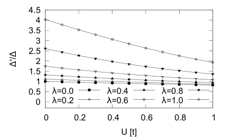
where is the effective bandwidth once interactions are taken into account, and is the Brillouin zone volume. This may be solved by using a binary search. The results for can be seen in Fig. 3. The effect of increased Coulomb repulsion is a small decrease in the effective gap. The effect of increased electron-phonon coupling is far more dramatic, and gap increases are seen for all at any value. I note that the enhancement increases as the bare gap, , decreases. Crucially, enhancement factors of can be seen for medium sized which could increase the moderate gaps seen experimentally in graphene on substrate systems to the eV gap sizes of silicon and germanium, with the caveat that changes in the form of the electron-phonon could quantitatively change this result. By changing the form of the superstrate or substrate, significant control could be exercised over the graphene band gap.
IV Low phonon frequency
Given the large gap enhancement in the large phonon frequency limit, it is appropriate to examine if the enhancement is present at low phonon frequency. It is not obvious that the intuitive gap enhancement seen at large phonon frequencies should still occur at low frequencies where retardation effects could lead to large pairs that are not localized. For low phonon frequency and weak coupling, low order perturbation theory can be applied. I derive a set of self-consistent equations assuming the following ansatz for the self energy,
Here, the momentum independent form of the ansatz (local approximation) is reasonable because of localization by the modulated potential and the electron-phonon interaction. Off diagonal terms are absent because they do not feature in the lowest order perturbation theory. The quasi-particle weight, , is shorthand for and is the gap function. Matsubara energies for Bosonic quantities are and for Fermions are , where is the temperature and and are integers.
The non-interacting graphene Green function in the presence of a modulated potential has the form,
| (4) |
The full Green function can be established using Dyson’s equation , leading to,
| (5) |
Substituting the expression for the Green function into the lowest order contribution to the self energy,
| (6) |
Here, the phonon propagator, . The off diagonal elements of the lowest order self energy are zero in the case of local interaction, so they do not feature in the ansatz. Since there is a modulated potential, it is necessary also to take into account the tadpole diagram (which has a contribution since the effects of the modulated potential can not simply be absorbed into the chemical potential) leading to the following Eliashberg style equations for and ,
| (7) |
| (8) |
and
| (9) |
where is the difference between the density of electrons on sites A and B and the full gap is . Here, the density of states for graphene in the absence of a gap, , has the form given in Ref. Neto et al., 2009. Note that these gap equations differ from those for a superconductor.
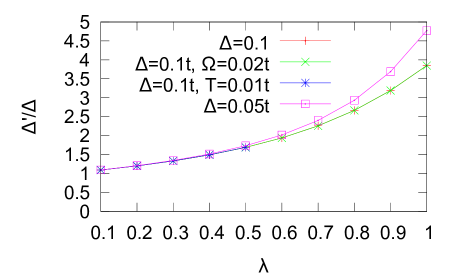
The equations may be solved self consistently by performing a truncated sum on Matsubara frequencies. The maximum Matsubara frequency was kept constant with the value, which is sufficiently large to ensure that asymptotic behavior of the gap function was achieved. The longest self-consistent solutions took around 2 weeks, increasing as and . The following parameters have been chosen to match graphene with a modest bare gap of the order of magnitude seen in the systems discussed in the introduction: corresponding to a gap of around 280meV, realistically achievable phonon energies of meV, and temperatures on the order of room temperature corresponding to K. The dynamical quasi-particle weight, is of order unity for all parameters considered here and the gap equation has very weak frequency dependence at the values of that have been considered.
The gap enhancement factor is shown in Fig. 4. Significant gap enhancement can be seen, with a swift rise at intermediate and achieving a factor 3 at around . The enhancement factor increases slightly with decreasing but is essentially unchanged by modifications to phonon frequency and temperature for the parameter values used here. I note that there may be some quantitative reduction to this enhancement for the longer range Fröhlich interaction. Consideration of electron-phonon couplings of up to the order of unity are reasonable since even in metals such as lead, the electron phonon coupling can be large () Reinert et al. (2003) and in the absence of interplane screening, even larger couplings should be possible. Therefore, gap sizes relevant to digital graphene devices should be achievable by placing ionic superstrates on top of e.g. the graphene on rubidium system, and such a system could make a good starting point for experimental investigations of the gap enhancement. It is noted that since rubidium is a conductor, an insulating material which leads to the same undressed gap would be necessary to make a working digital device. It is possible to rule out a number of materials which have been used for top and bottom gating in transport measurements. I note that gaps can also be induced in bilayer graphene McCann and Fal’ko (2006) and graphene nanoribbons Brey and Fertig (2006), so a similar mechanism of substrate mediated electron-phonon interaction may enhance gaps in those systems.
V Summary and conclusions
In summary, I have presented a theory for the enhancement of graphene band-gaps by polarizable superstrates. The theory predicts gap enhancements of up to 4 times from electron-electron interactions mediated through phonons in a polarizable ionic superstrate. The generation of sizable graphene bandgaps is a key problem for the use of graphene in many technologically important applications. The theory shows that the relatively simple addition of polarizable superstrates to graphene systems can provide a way of making large enhancements to graphene gaps. I suggest the following recipe for experimental investigation of an enhanced graphene gap: Form SiO2 or Si3N4 layers on top of graphene on ruthenium intercalated with gold. I note, however, that for digital applications an insulating substrate is required, so if the effect can be verified experimentally it will be necessary to find additional substrates that cause gaps in the graphene spectrum. It is hoped that this work will stimulate experiment, leading to tunable gapped graphene systems with applications in digital electronics, LEDs, lasers and photovoltaics.
VI Acknowledgments
I acknowledge EPSRC grant EP/H015655/1 for funding and useful discussions with P.E. Kornilovitch, A.S. Alexandrov, M. Roy, P. Maksym, E. McCann, V. Fal’ko, N.J. Mason, N.S. Braithwaite, A. Ilie, S. Crampin and A. Davenport.
References
- Zhou et al. (2007) S. Y. Zhou, G.-H. Gweon, A. V. Fedorov, P. N. First, W. A. D. Heer, D.-H. Lee, F. Guinea, A. H. C. Neto, and A. Lanzara, Nature Materials 6, 770 (2007).
- Enderlein et al. (2010) C. Enderlein, Y. S. Kim, A. Bostwick, E. Rotenberg, and K. Horn, New J. Phys. 12, 033014 (2010).
- Giovannetti et al. (2007) G. Giovannetti, P. A. Khomyakov, G. Brocks, P. J. Kelly, and J. van den Brink, Phys. Rev. B 76, 073103 (2007).
- Alexandrov and Kornilovitch (2002) A. S. Alexandrov and P. E. Kornilovitch, J. Phys.: Condens. Matter 14, 5337 (2002).
- Steiner et al. (2009) M. Steiner, M. Freitag, V. Perebeinos, J. C. Tsang, J. P. Small, M. Kinoshita, D. Yuan, J. Liu, and P. Avouris, Nature Nanotechnology 4, 320 (2009).
- Fratini and Guinea (2008) S. Fratini and F. Guinea, Phys. Rev. B 77, 195415 (2008).
- McCann and Fal’ko (2006) E. McCann and V. I. Fal’ko, Phys. Rev. Lett. 96, 086805 (2006).
- McCann et al. (2007) E. McCann, D. S. L. Abergel, and V. I. Falko, Solid State Communications 143, 110 (2007).
- Ohta et al. (2006) T. Ohta, A. Bostwick, T. Seyller, K. Horn, and E. Rotenberg, Science 313, 951 (2006).
- Zhang et al. (2009) Y. Zhang, T.-T. Tang, C. Girit, Z. Hao, M. C. Martin, A. Zettl, M. F. Crommie, Y. R. Shen, and F. Wang, Nature 459, 820 (2009).
- Fujita et al. (1996) M. Fujita, K. Wakabayashi, K. Nakada, and K. Kusakabe, J. Phys. Soc. Jpn. 65, 1920 (1996).
- Nakada et al. (1996) K. Nakada, M. Fujita, G. Dresselhaus, and M. S. Dresselhaus, Phys. Rev. B 54, 17954 (1996).
- Han et al. (2007) M. Y. Han, B. Özyilmaz, Y. Zhang, and P. Kim, Phys. Rev. Lett. 98, 206805 (2007).
- Kosynkin et al. (2009) D. V. Kosynkin, A. L. Higginbotham, A. Sinitskii, J. R. Lomeda, A. Dimiev, B. K. Price, and J. M. Tour, Nature 458, 872 (2009).
- Tao et al. (2011) C. Tao, L. Jiao, O. V. Yazyev, Y.-C. Chen, J. Feng, X. Zhang, R. B. Capaz, J. M. Tour, A. Zettl, S. G. Louie, H. Dai, and M. F. Crommie, Nature Physics 7, 616 (2011).
- Sofo et al. (2007) J. O. Sofo, A. S. Chaudhari, and G. D. Barber, Phys. Rev. B 75, 153401 (2007).
- Boukhvalov et al. (2008) D. W. Boukhvalov, M. I. Katsnelson, and A. I. lichtenstein, Phys. Rev. B 77, 035427 (2008).
- Charlier et al. (1993) J.-C. Charlier, X. Gonze, and J.-P. Michenaud, Phys. Rev. B 47, 16162 (1993).
- Elias et al. (2009) D. C. Elias, R. R. Nair, T. M. G. Mohiuddin, S. V. Morozov, P. Blake, M. P. Halsall, A. C. Ferrari, D. W. Boukhvalov, M. I. Katsnelson, A. K. Geim, and K. S. Novoselov, Science 323, 610 (2009).
- Cheng et al. (2010) S.-H. Cheng, K. Zou, F. Okino, H. R. Gutierrez, A. Gupta, N. Shen, P. C. Eklund, J. O. Sofo, and J. Zhu, Phys. Rev. B 81, 205435 (2010).
- MacDonald and Bistritzer (2011) A. H. MacDonald and R. Bistritzer, Nature 474, 453 (2011).
- Covaci and Berciu (2008) L. Covaci and M. Berciu, Phys. Rev. Lett. 100, 256405 (2008).
- Neto et al. (2009) A. H. C. Neto, F. Guinea, N. M. R. Peres, K. S. Novoselov, and A. K. Geim, Rev. Mod. Phys. 81, 109 (2009).
- Hague et al. (2006) J. Hague, P. Kornilovitch, A. Alexandrov, and J. Samson, Phys. Rev. B 73, 054303 (2006).
- Su et al. (1980) W. Su, J. Schrieffer, and A. Heeger, Phys. Rev. B 22, 2099 (1980).
- Lang and Firsov (1963) I. G. Lang and Y. A. Firsov, Sov. Phys.—JETP 16, 1301 (1963).
- Reinert et al. (2003) F. Reinert, B. Eltner, G. Nicolay, D. Ehm, S. Schmidt, and S. Hüfner, Phys. Rev. Lett. 91, 186406 (2003).
- Brey and Fertig (2006) L. Brey and H. A. Fertig, Phys. Rev. B 73, 235411 (2006).