The c-axis charge traveling wave in coupled system of Josephson junctions
Abstract
We demonstrate a manifestation of the charge traveling wave along the -axis (TW) in current voltage characteristics of coupled Josephson junctions in high- superconductors. The branches related to the TW with different wavelengths are found for the stacks with different number of Josephson junctions at different values of system’s parameters. Transitions between the TW branches and the outermost branch are observed. Time dependence of the electric charge in the superconducting layers and charge-charge correlation functions for TW and outermost branches show different behavior with bias current. We propose an experimental testing of the TW by microwave irradiation.
Many physical and biological objects may be considered as coupled nonlinear oscillators.strogatz93 Particularly, intrinsic Josephson junctions (JJ) in HTSC are studied from this point of view often.kleiner An attractive feature of intrinsic JJ is a generation of coherent radiation in terahertz region and it is investigated intensively.kleiner-science07 ; tsujimoto10 A coupling between junctions plays an important role. It leads to multiple branch structure in the current voltage characteristics (CVC) with additional to single junction parameters like the breakpoint (BP) current, the BP region width and the transition currents between branches.sm-sust07 ; matsumoto99 ; sm-prl07 ; smp-prb07 It was shown that the BP in CVC is a manifestation of the parametric resonance in this system when the Josephson oscillations create a standing longitudinal plasma wave perpendicular to the superconducting layers. The parametric resonance features were observed experimentally recently.iso-apl08
A well known feature of single long Josephson junction is the traveling wave along the barrier.kleiner It was notedkoyama96 ; machida98 that the system of capacitively coupled JJ has a plane wave which corresponds to the longitudinal Josephson plasma propagating perpendicular to the junctions. The sharp resonance peak in the microwave absorption spectrum obtained in Bi-2212 by Matsuda et al.matsuda95 has been identified with this collective Josephson plasma mode. Instability of the longitudinal plasma oscillations was discussed in Ref.machida98 and it was proposed that the multiple branches are caused by the freezing of the collective LPW into the static charge density wave.
In this letter we demonstrate the additional branch in CVC which corresponds to the charge traveling wave along c-axis (TW) when the junctions are in rotating states (phase differences are not small). Such branches were not investigated before. Transitions in hysteresis region from the outermost branch (OB) to the traveling wave branch (TWB) and between the TWB with different wavelengths are found. We demonstrate the appearance of the TWB at as well which originates from different branches of CVC including the zero voltage branch. A different dynamics of correlation functions for the TWB and for the OB is shown. We find the effect of the microwave radiation on TWB, which allows the experimental testing of this branch.
To simulate the CVC we investigate the phase dynamics in the framework of the capacitively coupled Josephson junctions with diffusion current (CCJJ+DC) model,machida00 ; sms-physC06 which is determined by the system of dynamical equations for the gauge-invariant phase differences between superconducting layers (-layers). Time is normalized to the inverse plasma frequency (), the voltage - to the value , the current - to the critical current . We consider the periodic boundary conditions in this paper. The structure of the simulated CVC in the CCJJ+DC model is equidistant in agreement with the experimental results.schlenga98 The details of simulation procedure are presented in Refssmp-prb07 ; shk-prb09
The manifestation of the TWB is shown in Fig. 1, where we present the total branch structure of CVC for the stack with 10 coupled JJ at , . It was obtained by multiple sweeping of the bias current through the stack.sm-physC06 ; sm-sust07 ; smp-prb07 This CVC is characterized by switching all junctions to the rotating (R-) state at , large hysteresis, and multiple branching in the hysteresis region by switching the JJ to the oscillating (O-) state with the decrease of the bias current.
The inset (a) enlarges the part of CVC corresponding to the transition from the OB to the another branch. As we can see, there is one more branch additionally to the OB. We prove below that this is TWB. Such TWB was manifested in CVC of the stack with 10 JJ in Ref.sm-sust07 (see Fig.5), but it was not mentioned at that time.
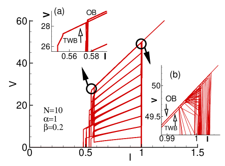
To see the origin of TWB we investigate a transition region in CVC near . In during of the sweeping bias current procedure we observe the jumps to the OB and TWB both from the zero voltage state directly and from the other branches of CVC. The inset (b) enlarges the part of CVC corresponding to this transition region.
The TWB have been observed in the stacks with different number of junctions. Particularly, the TWB in CVC were found in the stacks with 14 JJ and 28 JJ (Fig. 2), 9 JJ (Fig. 3d) and 7 JJ (Fig. 4). In case of even number of junctions in the stack, the jump from the OB to the TWB happens first to some unstable state. Such transition for stacks with 14 JJ at , is demonstrated in the inset (a) of Fig. 2, where a transition from the parametric resonance region of OB is observed. For the stacks with odd number of junctions we observe usually the jumps to the TWB from the chaotic part of breakpoint region in OB. The increase of bias current after jump instead of its decrease allows us restore the total TWB (see Fig. 3).
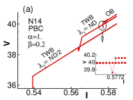
We note that the longest wavelength of a TW in the system with N JJ is , where D is a period of lattice ( the sum of thicknesses of insulating and superconducting layers). So, the waves with might appear in the stack, where n is devisor of number N. We stress that the TWB in Fig. 1 was naturally obtained just by sweeping of bias current. Another possibility is to use the variation of the initial conditions for phase differences. In Fig. 2 we show such realization of the TWB corresponding to TW with different wavelengths. Particularly, in Fig. 2a we demonstrate the manifestation of the TWB in CVC of the stacks with 14 JJ related to the waves with and . Inset demonstrates a transition of the OB to the first TWB with . The analysis of the time dependence of the charge in S-layers and its distribution along the stack around the second transition in Fig. 2a shows that the TW with transforms to TW with .
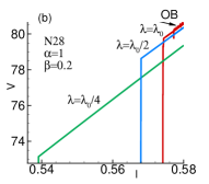
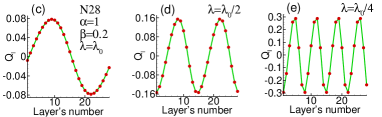
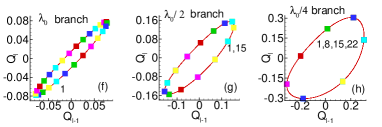
In Fig. 2(b) we demonstrate the TWB for the stack with N=28, corresponding to the states with wavelengthes , and . The different initial conditions for the phases and the voltages in the JJ were used to obtain these branches. We find the wavelength of the TW by the distribution of the charge in the S-layers along the stack at fixed time moment. Such distribution at bias current is shown in Fig. 2(c),(d) and (e). These figures demonstrate also that the amplitude of charge is greater for the TW with smaller wavelengths.
To test if these distributions follow precisely to the TW, we present in Fig. 2(f),(g) and (h) the corresponding Lissajous charge-charge diagrams. In fact, two different plots are shown in each figure: squares show the for different values of at fixed time moment; the curves show the trajectory for fixed value of in during a whole time domain (i.e., the time domain at constant value of current). We got the same curve for different , which means that the charge in each layer has the same frequency and amplitude, but the charge in layers differers by a phase shift only. So, this wave is not a standing wave, but a traveling one.
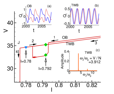
An example of the charge dynamics corresponding to the OB and TWB for the stack with 9 JJ at and and its simulation procedure is demonstrated in Fig. 3. First we follow the OB (arrow 1), decreasing the current from the value I=1.2. At I=0.78405 a transition from the chaotic part of OB to TWB is happened. We continue the current decreasing process along TWB till the I=0.78. At this point we increase current (arrow 2), follow the TWB till . Then we return back (arrow 3) and follow along the TWB till the jump to the another branch (arrow 4). The insets (a,b) show a time dependence of charge in first (solid line) and second (dashed line) S-layers of the stack at for the OB and TWB, correspondingly. We see that in the case of TWB the charge oscillations in S-layers are just shifted in phase. In the supplement we present the animation of the charge-time dependence demonstrating the traveling wave along the stack. The inset (c) presents the result of FFT analysis of charge-time dependence corresponding to the TWB. The time domain was taken at I=0.792, where the value of voltage is equal to V=32.956. As we see the value coincide with the results of FFT analysis .
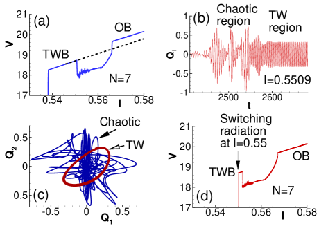
One more manifestation of the TWB is shown in Fig. 4, where we demonstrate a transition to the TWB for the stack with 7 JJ at . The charge-time dependence demonstrates a changing of character of the charge oscillations in S-layer near a transition point at I=0.5509 (Fig. 4b). We can see the transformation of the chaotic behavior in the OB to the regular one in TW state. In Fig. 4c we show the Lissajous charge-charge diagram in chaotic (thin line) and TW (thick line)regions. The diagram demonstrate the variation in time of the charges in two neighbor layers. The charge in the first S-layer is plotted along the x-axis and charge in the second one along the y-axis. As we can see, the Lissajous charge-charge diagram presents an open trajectory for the chaotic region and closed one for the TW region.
We find the effect of microwave radiation on TWB, which was taken into account by the including an additional current through the stack. Increasing power of radiation (amplitude A) leads to the destroying of the TW and transition from the TWB to the another branch in CVC. In Fig. 4d we demonstrate the effect of radiation, which was switch on at with amplitude and Josephson frequency . As we can see, the TWB disappears under this radiation. This result open a way for the experimental testing the observed branches in CVC.
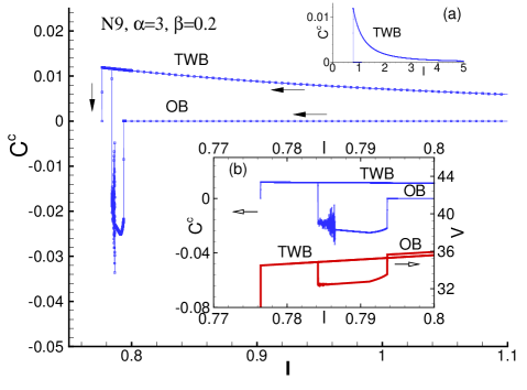
To compare dynamical behavior of the states corresponding to the OB and TWB in long bias current interval, we have made a correlation functions analysisshk-prb09 . We have investigated a correlation of charge in neighboring layers by charge-charge correlation functions . Fig. 5 shows the dependence of correlation function ”charge-charge” for neighbor layers three and four on bias current for the OB and the TWB. We stress that all curves were obtained in the one numerical experiment. Inset (a) demonstrate the increase of correlations () in the TW state with decreasing of the bias current in the large interval of . As it has been seen from the inset (b) which enlarges the region near BP, the correlation functions for the OB demonstrate the characteristic BPR structure with the features obtained in the Ref.shk-prb09 . We see also that the features of correlation functions coincide with the features of CVC. The for TWB are coincide for all . The correlation functions current-current (not presented here) show the same behavior. The autocorrelation functions for TW state, which are defined by , have a constant amplitude, i.e., the system in the state with TW is complectly self repeating.
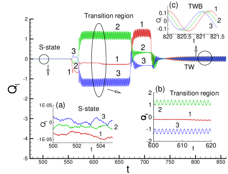
Finally, let us describe shortly the creation of the TWB at . In Fig. 6 we present the charge-time dependence in transition region around (see the inset (b) in Fig. 1) for three S-layers in the stack with 10 JJ. We enlarged the dependence in this region and show it in three insets separately: the inset (a) shows it in zero-voltage state, inset (b) - in some part of the transition region shown by oval, inset (c) - in the state with TW. The simulation was done by increase a bias current in the interval around with a step in current . We observe here a complex dynamical behavior in a very short time interval inside of the time domain. Fluctuations of charge in S-layers in zero voltage state is replaced by specific changes of the charge and the oscillations with nonzero time averaged value (charge value in S-layer is high enough, up to ), then we see a transition to the TW state. The amplitude of charge oscillations in TW state is large, but its average in time is zero. A detailed description of the switching dynamics will be presented somewhere else.
In summary, we showed that CVC of coupled Josephson junctions has the branches related to the charge traveling waves along the c-axis. Transitions between such branches demonstrating the changing of wavelength of the traveling wave with a decrease of bias current were found. We fixed also the transitions from the outermost branch to the traveling wave branch. Detailed analysis of the time dependence of the charge in superconducting layer, its FFT analysis and the investigations of correlation functions showed different features of such transitions, particularly, different behavior for the outermost and traveling wave branches. These results shed light on the resonance features of the coupled Josephson junctions which are investigated intensively today. The detailed analysis of the branch structure in the experimental CVC of IJJ has not been done yet. We proposed a method to distinguish the branch related to the charge traveling wave along c-axis from the other branches in CVC by microwave irradiation.
We thank R. Kleiner, A. Yurgens, V. Krasnov, M. Suzuki, F. Mahfouzi and M. R. Kolahchi for helpful discussions.
References
- (1) S.H.Strogatz and I.Stewart, Sci.Am. 269 102 (1993).
- (2) W. Buckel, R. Kleiner, Superconductivity. Fundamentals and Applications, Wiley-VCH Verlag GmbH Co, KGaA, (2004).
- (3) R. Kleiner, Science 318, 1254 (2007).
- (4) M. Tsujimoto et al., Phys. Rev. Lett. 105, 037005 (2010).
- (5) Yu. M. Shukrinov, F. Mahfouzi, Phys.Rev.Lett. 98, 157001 (2007).
- (6) H.Matsumoto et al., Phys. Rev. B 60, 3666 (1999).
- (7) Yu. M. Shukrinov, F. Mahfouzi, Supercond. Sci.Technol., 19, S38-S42 (2007).
- (8) Yu. M. Shukrinov, F.Mahfouzi, N. F. Pedersen, Phys. Rev. B 75, 104508 (2007).
- (9) A. Irie, Yu. M. Shukrinov, G. Oya, Appl.Phys.Lett. 93, 152510, (2008).
- (10) T. Koyama and M. Tachiki, Phys. Rev. B 54, 16183 (1996).
- (11) M. Machida, T. Koyama, and M. Tachiki, Physica C300, 55 (1998).
- (12) Y. Matsuda et al., Phys. Rev. Lett. 75, 4512 (1995).
- (13) M. Machida, T. Koyama, A. Tanaka and M. Tachiki, Physica C330, 85 (2000).
- (14) Yu. M. Shukrinov, F. Mahfouzi, P. Seidel. Physica C449, 62 (2006).
- (15) Schlenga K. et al., Phys.Rev. B 57(1998) 14518.
- (16) Yu. M. Shukrinov, M. Hamdipour, M. Kolahchi, Phys.Rev. B 80, 014512 (2008).
- (17) Yu. M. Shukrinov and F. Mahfouzi, Physica C434, 6 (2006).