Interlayer binding energy of graphite – A direct experimental determination
Abstract
Despite interlayer binding energy is one of the most important material properties for graphite, there is still lacking report on its direct experimental determination. In this paper, we present a novel experimental method to directly measure the interlayer binding energy of highly oriented pyrolytic graphite (HOPG). The obtained values of the binding energy are 0.27(0.02)J/m2, which can serve as a benchmark for other theoretical and experimental works.
pacs:
Valid PACS appear hereSince the successful fabrication of monolayer graphene from highly oriented pyrolytic graphite (HOPG) in 2004 1 , great interests have been attracted by this perfect two-dimensional crystal made of carbon atoms. The superior electronic, thermal, and mechanical properties, and the large specific surface area make it a promising component in next generation of electronic devices, energy storage and conversion devices, water treatment application, and the smart (bio) materials 2 ; 3 ; 4 ; 5 . Its inherent single layer structure determines that the application of graphene, to a large extent, rely on the detailed understanding and control of it interacts with its surroundings 6 . However, the nature and strength of interlayer binding in graphitic materials are poorly understood, despite that the binding strength in graphite/graphene is relevant to many key applications, such as graphene electronic devices fabricated on various substrates, graphite intercalation compounds in Li battery, carbon based system for hydrogen storage, and graphene based supercapacitors.
Experimentally, there is still lacking report on direct measurements of graphite interlayer binding energy (BE) and exfoliation energy (EE, the energy required to remove one graphene layer from a single-crystalline graphite) 7 . Although there are few reported values obtained indirectly, those values are quite discrepant. Based on the heat of wetting data, Girifalco et al. 8 obtained the EE value as 435 meV/atom (or 0.260.03J/m. By assuming the simple Lennard-Jones potential, they further estimated the BE to be about 18% larger than the EE, while the exact difference remains unknown. Benedict et al. 9 extrapolated the BE as meV/atom (or J/m from the measurement on the collapsed carbon nanotubes. More recently, Zacharia et al. 10 performed desorption experiments of aromatic molecules from a graphite surface and obtained the approximate graphite EE = 525 meV/atom (or 0.320.03J/m, which yields an estimate of the BE 0.37 J/m2.
Theoretically, modeling BE as well as EE for graphite is still a question mark due to the weak interlayer binding involving van der Waals interaction, which remains a notorious difficult to describe within the standard density functional theory (DFT) 7 ; 11 . The standard approximations used in DFT, such as local density approximation (LDA) and generalized gradient approximation (GGA), cannot accurately describe the long distance interaction such as van der Waals interactions. LDA calculations lead to good interlayer distance (e.g., 0.33nm) but binding energy is predicted as low as 24meV/atom (or 0.15 J/m2) 12 . An alternative is the van der Waals density functional method, which is developed to account the long-range part of the interactions by using an explicit nonlocal functional of density. However, the predicted interlayer distance is substantially higher than experimental value (e.g., 0.36, 0.376, vs. 0.334nm), the elastic modulus C33 is significantly lower (e.g., 13, 27 vs. 36GPa), and the binding energy is very scattered (e.g., 24meV/atom (or 0.15 J/m, 45.5 meV/atom (or 0.28 J/m, and 50 meV/atom (or 0.30 J/m2)) 12 ; 13 ; 14 . Until recently, two comprehensive first-principles calculations have been carried out. Spanu et al. 7 has employed the quantum Monte Carlo method to obtain the binding energy about 56meV/atom (or 0.34 J/m, and Lebegue et al. 11 has used the adiabatic-connection fluctuation-dissipation theorem in the direct random approximation to obtain the binding energy as 48meV/atom (or 0.29 J/m.
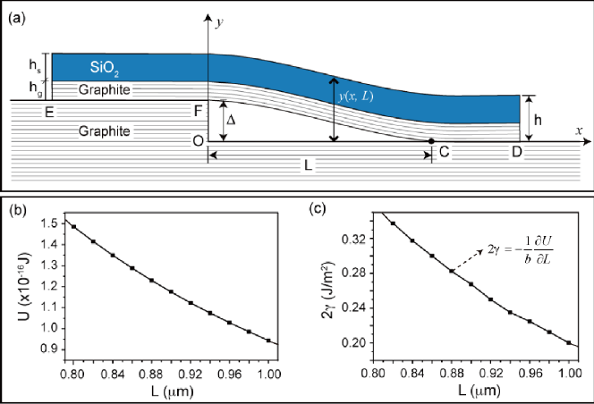
The above brief review shows a clear need of directly experimental determination of the BE for graphite. In this paper, we introduce a novel method to directly measure BE, which is motivated by our recent discovery of self-retraction motion phenomenon of micrometer graphite/SiO2 flakes on graphite islands 15 . The idea is to assemble a thin graphite flake to span over a graphite step. As illustrated in Fig.1(a), the considered graphite flake consists of multilayered graphenes assembled in AB-stack, and the graphite step is single-crystalline with atomically smooth graphene top surfaces. The key of this experimental technique is to make the contact areas (C-D and E-F indicated in Fig. 1(a)) between the flake and the step in the AB-stack assembling. In our experiments, each graphite flake was coated on its top surface with a SiO2 thin film. The deformation energy of the above of graphite/SiO2 flake and graphite step can be modeled as a function of the step height , the span length , the thicknesses and of the SiO2 film and the graphite flake, and the material elastic constants. Since a virtual increment of length leads to the increase of the graphite surface area 2 and, consequently, the increment of the total surface energy 2, where denotes the flake width and is the graphite basal plane surface energy, we obtain the equilibrium equation of the above system in the following form:
| (1) |
Using the above-proposed method, we measured the interlayer binding energy, namely 2, of HOPG to be 0.270.02 J/m2 (or 443 meV/atom). The details of our experiments are reported below.
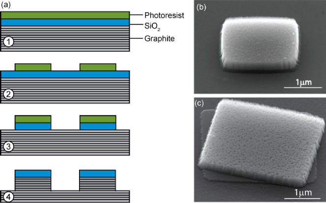
The HOPG samples were purchased from Veeco (ZYH grade). As illustrated in Fig. 2(a), graphite islands were fabricated by using the same technique as that reported in Ref. 16 . After mechanical exfoliation, a clean and fresh top surface of the HOPG sample was obtained 17 . A silicon dioxide (SiO film was then grown on the sample top surface by plasma enhanced chemical vapor deposition (PECVD), and then followed by electron beam lithography and reaction ion etching. Figure 2(b) shows the scanning electron microscopy (SEM, FEI Quanta 200F) image of an obtained island with typical length 2-5m and height 400nm. Figure 2(c) is the SEM image of the side-view of an island with the top flake tilted 30 degrees.
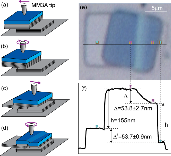
Similar to Ref. 15 , we employed a micromanipulator MM3A (Kleindiek) that had been set in a SEM (FEI Quanta 200F) to perform our experiments under an ultrahigh vacuum condition (1.19 - 6.7210-4 Pa) and the room temperature. Electron beam with 30 KV acceleration and 3 nm spot-size was used to monitor the fabrication process. The in situ process can be seen from Supplementary Movie. Schematically we show the experimental process in Fig. 3. We placed the MM3A tip on the top surface of a selected island and then pushed it in a lateral direction (Fig. 3(a)). A graphite/SiO2 flake was then sheared out from its platform (base flake of the graphite island). The flake was found to be fully self-retractable after removing the tip. Our study on the self-retraction mechanism has revealed that the slipping plane corresponds to a boundary between two single-crystalline graphite grains and the original assembling between the moved flake and platform (before shear) is not AB-stacked, which leads to the large-scale superlubricity 15 ; 18 and consequently the self-retraction motion. To prevent the self-retraction, we used the tip to rotate the flake for a certain angle until the flake was suddenly locked up, which corresponds to an AB-stack assembling as revealed in our recent study 18 . In the experiment, pushing the locked top flake again in the opposite lateral direction leads to the separation of the flake into two parts: the top and the middle flakes. The observed self-retraction between these two separated flakes (See Supplementary Movie) indicates once more a non AB-stack contact. To prevent the self-retraction, we rotated the top flake with respect to middle flake to another ‘lock-up’ state (Fig. 3(d)), and finally two flakes over the platform are both locked-up.
The optical microscope (OM, HiRox KH-3000) image of a typical locked-up example in our experiments is shown in Fig. 3(e), where the top flake (blue colored) spanned over the middle graphite flake. Fig 3(f) shows the height profile along the black line in Fig. 3(e), obtained by using an atomic force microscope (AFM). The measured step height or the middle flake thickness is * = 53.70.9 nm. In comparison, the height drop along the top flake surface was measured as = 53.82.7 nm, which is almost the same as the thickness of the middle flake. Such a good agreement confirms the good adhesion of the top flake with the middle flake and platform. This negligible difference could come from the surface roughness of the SiO2 thin film. The good adhesion is also supported by colour image in Fig. 3(e), where the blue color is fully reproduced at both flat sides of the top flake.
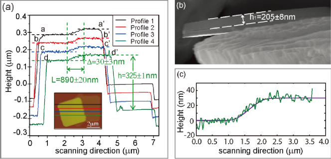
Figure 4(a) shows the AFM measured height profiles along the lines in the insert for the sample prepared in SEM as explained before. The thickness of the top flake is measured as = 3251nm and the height of the step (i.e., the thickness of the middle flake) is = 303 nm. By using MM3A micromanipulator to take the top flake off its platform and then stand the flake up, we measured the thickness of the SiO2 film as 2058 nm (Fig. 4(b)). Using the measured values = 30nm, = 205nm, = 120nm, and well-accepted elastic constants of SiO2 and graphite in our finite element (FEM) model (see details in Supplementary Information), we obtained the deflection curve , of the top surface of the model graphite/SiO2 flake at different span length . Finally, we can quite accurately determine the span length of each AFM measured height profile by least square fitting it to the , results obtained from our FEM analysis. The actual in our experiments should correspond to the value with the least fitting error. One example of such fitting is given in Fig. 4(c) with the fitted span lengths = 890 nm. The error bound of is estimated smaller than 20nm.
It should be noted that expressing the elastic strain energy in Eq. (1) by an analytic model is rather difficult due to the following two aspects. First, the bulk graphite has the highest elastic anisotropy 19 : the highest in-plane elastic modulus (e.g., 1000GPa) and very weak interlayer shear modulus (e.g., 4.5GPa). The shear deformation near the interface between SiO2 film and graphite flake is expected to be significant and difficult to theoretically model. Second, the elastic deformation of the step (made up by the middle flake and the platform) is difficult to describe as well, although it turns out to be important. Finite element method (FEM) analyses were thus employed to calculate the strain energy . The details of FEM model are included in Supplementary Information (SI). Figure 1(b) plots the calculated strain energies and Fig. 1(c) gives the approximations of BE through following central finite difference of Eq. (1):
| (2) |
with = 20 nm. Finally, the binding energy is approximated as 0.27 0.02 J/m2, corresponding to determined length = 890 20 nm (Fig. 1 (c)).
To test the reliability of the above-proposed method, we measured the second island sample with different size and shape. The measured binding energy is 0.30 0.025 J/m2, which agrees pretty well with the first sample shown in Figure 4(a). Details are given in SI.
It is well known that chemisorption, physisorption, and insertion of gases inside graphite can drastically change the surface/interface properties 20 . The binding energy of graphite under vacuum was estimated about 100 times higher those in an environment with air, oxygen or water vapor 21 . To avoid such artificial effects, we note again that above-reported experiments are carried out in SEM with ultra-high vacuum condition. Similar experiments but in atmospheric conditions were also done using an MM3A assisted by an optical microscope. The binding energy measured is just a little smaller than that from SEM, 0.22J/m2. We believe that the self-retraction motion of graphite/SiO2 flakes can self-clean the adsorbate on the exposed sliding surfaces 22 .
In summary, a novel experimental method is presented here to directly measure the interlayer binding energy of highly oriented pyrolytic graphite: 2 = 0.27 0.02 J/m2 (or 44 3 meV/atom). The error bar is mainly caused by the roughness of the top SiO2 thin film. It can be improved significantly by either extracting a smoother deflection profile from comparison of the AFM height profiles along lines on top flakes before and after its spanning over the step, or simply using other types of top thin films and improved ion etching process. Our proposed method can be easily extended to measure the binding energies between the graphite/graphene and other types of substrates. It can also be used in other systems, particularly lamellar materials and thin films. Considering the difficulty in measuring the interface binding energy in micro/nano-materials, our method could serve as a general solution.
Q.S.Z. acknowledges the financial support from NSFC through Grant No. 10832005, the National Basic Research Program of China (Grant No. 2007CB936803), and the National 863 Project (Grant No. 2008AA03Z302). J.Z.L. acknowledges new staff grant 2010 and small grant 2011 from engineering faculty of Monash University.
References
- (1) K. S. Novoselov et al., Science 306, 666 (2004).
- (2) A. K. Geim, Science 324, 1530 (2009).
- (3) A. K. Geim, et.al., Nat. Mater. 6, 183 (2007).
- (4) M. D. Stoller, et.al., Nano Lett., 8, 10 (2008).
- (5) N. Mohanty, et.al., Nano Lett., 8, 12 (2008).
- (6) X. Du, et.al., Nat. Nanotechnology 3, 491(2008).
- (7) L. Spanu, et.al., Phys. Rev. Lett. 103, 196401 (2009).
- (8) L.A. Girifalco, et.al., J. Chem. Phys. 25, 693(1956).
- (9) L. Benedict et al., Chem. Phys. Lett. 286, 490 (1998).
- (10) R. Zacharia, et.al., Phys. Rev. B 69, 155406 (2004).
- (11) S. Lebegue, et.al., Phys. Rev. Lett. 105, 196401 (2010).
- (12) M. Dion, et.al., Phys. Rev. Lett. 92, 126402 (2004).
- (13) E. Ziambaras, et.al., Phys. Rev. B 76, 155425 (2007).
- (14) S. D. Chakarova-Kack, et.al., Phys. Rev. Lett. 96, 146107 (2006).
- (15) Q.S. Zheng, et.al., Phys. Rev. Lett. 100, 067205 (2008).
- (16) X.K. Lu et al., Nanotechnology 10, 269 (1999).
- (17) Z. Liu, et.al., Appl. Phys. Lett. 96, 201909 (2010).
- (18) Z. Liu et al., Self-retracting motion of graphite micro-flakes: superlubricity in micrometer scale (submitted, see also:)
- (19) L. F. Wang, et.al., Appl. Phys. Lett. 90, 153113 (2007).
- (20) H. Zaidi, et.al., Thin Solid Films, 264, 46 (1995).
- (21) P. J. Bryant, et.al., Mechanics of Solid Friction (Elsevier, Amsterdam, 1964).
- (22) Z. Liu, et.al., Graphite nanoeraser, Nanotechnology (revised version under review, see also: http://arxiv.org/abs/1010.4102).