Laterally proximized aluminum tunnel junctions
Abstract
This letter presents experiments on junctions fabricated by a new technique that enables the use of high quality aluminum oxide tunnel barriers with normal metal electrodes at low temperatures. Inverse proximity effect is applied to diminish the superconductivity of an aluminum dot through a clean lateral connection to a normal metal electrode. To demonstrate the effectiveness of this method, fully normal-state single electron transistors (SET) and normal metal-insulator-superconductor (NIS) junctions applying proximized Al junctions were fabricated. The transport characteristics of the junctions were similar to those obtained from standard theoretical models of regular SETs and NIS junctions.
An important element in nanoelectronic circuits is a tunnel barrier between two leads, with applications ranging from superconducting qubits makhlin01 and quantum metrology devices pekola08 to electronic refrigeration by hybrid normal metal-insulator-superconductor (NIS) junctions giazotto06 ; nahum94 ; leivo96 ; clark04 . A standard material for yielding high quality junctions is aluminum due to rapid oxidation of its surface into a thin and stable layer of insulating aluminum oxide (AlOx) under oxygen exposure. Aluminum is superconducting below the critical temperature 1.2 K in bulk and up to 2.7 K in thin films adams04 . High-quality nano-scale junctions are typically fabricated in a single vacuum cycle by shadow evaporation of metals at multiple angles through a suspended mask dolan77 , combined with in situ oxidation. Depositing a layer of normal or superconducting material on top of oxidized Al forms a NIS or a superconductor-insulator-superconductor (SIS) junction.
Regrettably, fabrication of low temperature normal metal-insulator-normal metal (NIN) junctions or NIS junctions with non-Al superconductor is not straightforward. The latter would be beneficial in terms of controlling the through the choice of material: a higher would benefit for example a current standard based on the hybrid SINIS turnstile pekola08 , while a lower would be efficient for low temperature NIS coolers giazotto06 , where the optimal cooling power is at . In order to use Al for either NIN junctions or NIS junctions with non-Al superconductor, its superconductivity must be suppressed. Alternatively, aluminum can be isotropically deposited as a thin layer on top of the N electrode, after which it is thoroughly oxidized before depositing the counterelectrode gueron96 . When applied with shadow evaporation the latter technique, however, requires caution to ensure uniform Al coverage to avoid short circuits.
The aluminum superconductivity may be suppressed by various means, such as by applying a magnetic field. However, magnetic fields are not always desirable when combining NIN and NIS junctions on a single circuit, for example when combining normal-state SETs with NIS thermometers and coolers kubala08 . Although it is possible to have both NIN and NIS Al-based junctions in a single circuit by controlling the thicknesses and thus the critical fields of Al layers greibe11 , in some applications external fields cannot be tolerated. Another approach is to dope Al with e.g. manganese impurities to control or diminish the while retaining the BCS density of states clark04 ; oneil08a , but the junction quality could be compromised oneil10 . Also the use of inverse proximity effect arising in a normal metal-superconductor (NS) bilayer is a widely used technique for modifying the superconductor buzdin05 ; gupta04 : the normal metal gains a superconducting character, while the superconductor gains normal metal features at a short distance from the interface buzdin05 ; pannetier00 .
This letter introduces a new technique for suppressing the Al superconductivity in small tunnel junctions, by utilizing the inverse proximity effect in lateral direction. According to the theory of diffusive, inhomogeneous proximity superconductivity belzig99 , the superconductivity is fully suppressed in a NSN structure with infinite-size N reservoirs, when the length of the quasi-1D S-material wire radovic91 ; liniger93 . By symmetry, for a NS structure the suppression is achieved for . Utilizing our fabrication process the Al film superconducting coherence length is typically nm courtois08 ; peltonen10 , yielding nm. When accounting the non-ideal interface, a short Al wire with nm, proximized by a long normal metal lead, forms a high-quality NIN or NIS tunnel junction.
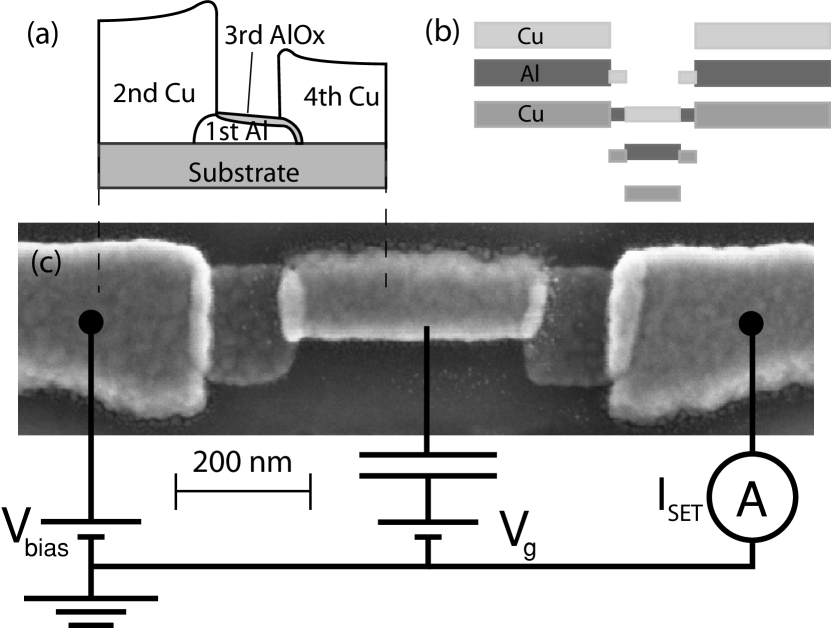
The proximized Al junctions were utilized in the fabrication of several normal-state SET samples with multi-angle shadow evaporation, for which the mask layout is shown in Fig. 1 . Figure 1 sketches a cross-section of a proximized Al junction that is used in the sample. The fabrication process had the following order, illustrated in Fig. 1 : first a 15 nm layer of aluminum is evaporated to form two small Al dots 400 nm apart, directly followed by a thick (45 nm) copper in a different angle to partially cover the dot with a proximizing normal metal lead. Third, the remaining uncovered aluminum is oxidized in the evaporation chamber, after which the SET is formed by depositing a 30 nm copper layer at a third angle to contact the two Al dots.
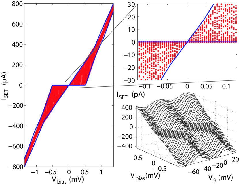
The suppression of the Al dot superconductivity was examined by measuring the current as a function of applied bias and gate voltages, and , respectively, according to the circuit diagram in Fig. 1 . The samples were measured in a 3He -4He dilution refrigerator pekola94 with a base temperature close to 40 mK. The results for the SET of Fig. 1 with highest charging energy eV are shown in Fig. 2. All of the measured structures showed similar behavior. Figures and show the range over which varies as is swept, fit by a standard SET model curve based on the orthodox theoryaverin86 , with the inclusion of asymmetric junction resistances, . The linearity at low bias voltages for maximum current indicates that the leads in the SET are normal, for otherwise there would be a gate-independent zero-current region for .pekola08 This is further supported by Fig. 2 , which shows as a function of both and , demonstrating the Coulomb diamonds characteristic to a normal SET.
Another more demanding test of the quality of a proximized junction is to utilize them in a NIS junction. The magnitude of subgap features, such as supercurrent through the junction, is an excellent indicator for determining the superconductivity of the Al dot. Also the differential conductance of the junction at low is directly proportional to the superconductor density of states if the counterelectrode is at normal state. The NIS junction samples are fabricated like the NIN junctions of the SET described earlier, with Al as the S lead and copper as the N lead, yet these could be replaced by other normal and superconducting metals.
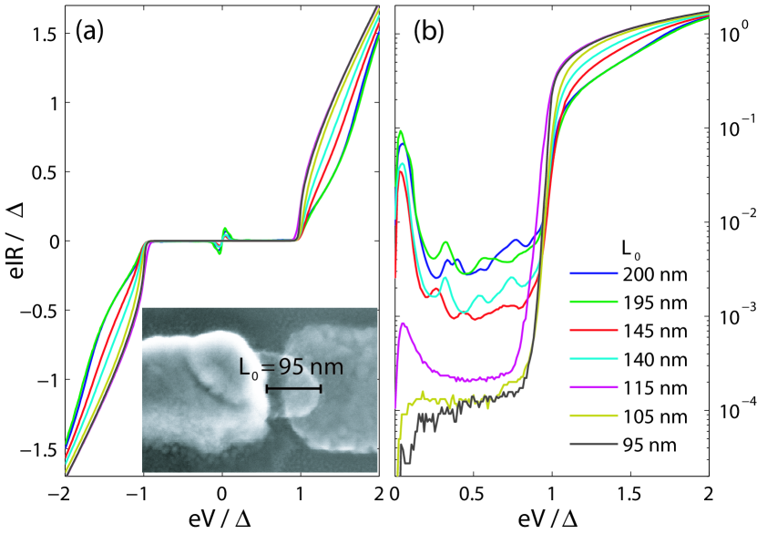
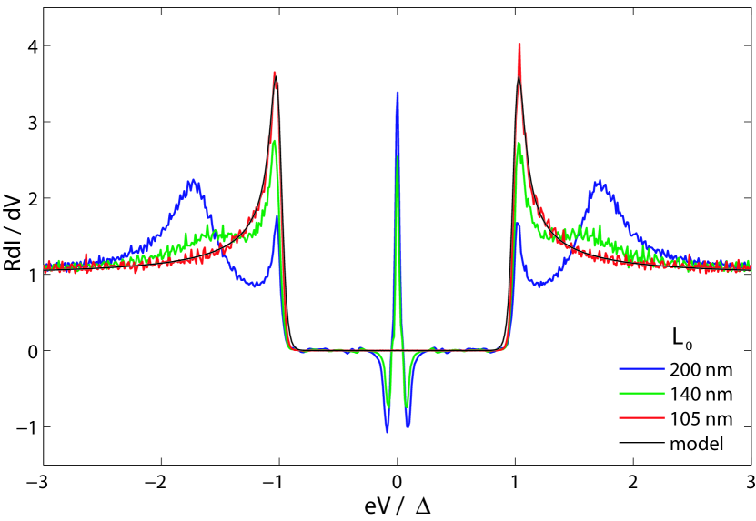
Several NIS junctions were fabricated simultaneously with various , the length of Al dot uncovered by the normal electrode. The NS contact and tunnel junction overlap areas were kept constant. The inset of Fig. 3 shows a SEM image of the structure with the shortest nm. The measured normal state resistances of the junctions were in the range of k and the zero temperature superconductor energy gap of the S - Al was eV. Figure 3 shows the measured current-voltage (IV) characteristics at mK. Additionally, Fig. 4 shows the differential conductance of several samples obtained by numerical differentiation of the IV data together with a theoretical fit for a standard NIS junction. Finally, the IV characteristics of the nm sample in the temperature range of mK are plotted in Fig. 5, together with theoretical curves using a phenomenological Dynes parameter dynes84 in the Al quasiparticle density of states.
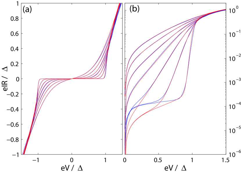
In these figures the dependence on the length of the Al dot is clearly visible: with nm they appear to have mixed NIS and SIS junction properties with notable supercurrent peaks, but as the dot length approaches 100 nm, both the IV curve and the differential conductance resemble increasingly those of a regular NIS junction. The results suggest that proximized Al tunnel junctions provide a valid tool for fabricating NIS junctions, where the superconductor is not necessarily aluminum. Such structures have been a challenge to fabricate by shadow evaporation till now.
Concluding, the method of forming tunnel junctions with the help of laterally proximized Al was introduced. These junctions were implemented in a fully normal SET and individual NIS junction configurations. The measured IV characteristics would indicate that the presented method is likely to allow shadow fabrication of high quality NIN junctions, as well as NIS junctions with non-Al superconductor.
We acknowledge financial support from the European Community’s FP7 Programme under Grant Agreement No. 228464 (MICROKELVIN, Capacities Specific Programme) and No. 218783 (SCOPE). We thank T. Heikkilä and P. Virtanen for discussions.
References
- (1) Yu. Makhlin, G. Schön, and A. Shnirman, Rev. Mod. Phys. 73, 357 (2001).
- (2) J. P. Pekola et al., Nature Phys. 4, 120 (2008).
- (3) F. Giazotto et al., Rev. Mod. Phys. 78, 217 (2006).
- (4) M. Nahum, T. M. Eiles, and J. M. Martinis, Appl. Phys. Lett. 65, 3123 (1994).
- (5) M. M. Leivo, J. P. Pekola, and D. V. Averin, Appl. Phys. Lett. 68, 1996 (1996).
- (6) A. M. Clark et al., Appl. Phys. Lett. 84, 625 (2004).
- (7) P.W. Adams, Phys. Rev. Lett. 92, 067003 (2004).
- (8) G. J. Dolan, Appl. Phys. Lett. 31, 337 (1977).
- (9) S. Guéron et al., Phys. Rev. Lett. 77, 3025 (1996).
- (10) B. Kubala, J. König, and J. P. Pekola, Phys. Rev. Lett. 100, 066801 (2008).
- (11) T. Greibe et al., Phys. Rev. Lett. 106, 097001 (2011).
- (12) G. O’Neil et al., Phys. Rev. Lett. 100, 056804 (2008).
- (13) G. O’Neil et al., J. Appl. Phys. 107, 093903 (2010).
- (14) A. I. Buzdin, Rev. Mod. Phys. 77, 935 (2005).
- (15) A. K. Gupta et al., Phys. Rev. B 69, 104514 (2004).
- (16) B. Pannetier and H. Courtois, J. Low Temp. Phys. 118, 599 (2000).
- (17) W. Belzig et al., Superlattices Microstruct. 25, 1251 (1999).
- (18) Z. Radović et al., Phys. Rev. B 44, 759 (1991).
- (19) W. Liniger and J. Low Temp. Phys. 93, 1 (1993).
- (20) H. Courtois et al. Phys. Rev. Lett. 101, 067002 (2008).
- (21) J. T. Peltonen et al., Phys. Rev. Lett. 105, 097004 (2010).
- (22) J. Pekola and J. Kauppinen, Cryogenics 34, 843 (1994).
- (23) D. V. Averin and K. K. Likharev, J. Low Temp. Phys. 62, 345 (1986).
- (24) R. C. Dynes et al., Phys. Rev. Lett. 53, 2437 (1984).