Large-area, wide-angle, spectrally selective plasmonic absorber
Abstract
A simple metamaterial-based wide-angle plasmonic absorber is introduced, fabricated, and experimentally characterized using angle-resolved infrared spectroscopy. The metamaterials are prepared by nano-imprint lithography, an attractive low-cost technology for making large-area samples. The matching of the metamaterial’s impedance to that of vacuum is responsible for the observed spectrally selective “perfect” absorption of infrared light. The impedance is theoretically calculated in the single-resonance approximation, and the responsible resonance is identified as a short-range surface plasmon. The spectral position of the absorption peak (which is as high as ) is experimentally shown to be controlled by the metamaterial’s dimensions. The persistence of “perfect” absorption with variable metamaterial parameters is theoretically explained. The wide-angle nature of the absorber can be utilized for sub-diffraction-scale infrared pixels exhibiting spectrally selective absorption/emissivity.
I Introduction
The field of electromagnetic metamaterials (MMs) has been rapidly developing in recent years. New composite materials with sub-wavelength size and exotic electromagnetic properties generally unattainable in nature Veselago (1968); Smith et al. (2000); Pendry (2000); Schurig et al. (2006) are being designed and produced for many applications such as perfect lenses Pendry (2000), cloaking devices Schurig et al. (2006), sub-wavelength transmission lines and resonators Alu and Engheta (2004), and agile antennas Chen et al. (2008). Another important application of MMs is the development of spectrally selective “perfect” absorbers Landy et al. (2008a) (near-unity peak absorptivity). Such absorbers can be used for developing sensitive detectors for a variety of security-related applications, as well as narrow-band thermal emitters for thermophotovoltaic (TPV) Coutts (1999); Laroche et al. (2006) applications. In photovoltaic (PV) applications, ultra-thin MM absorbers can be applied on surfaces of thin-film solar cells to reduce reflectivity Tvingstedt et al. (2007), thereby increasing the external quantum efficiency.
Miniaturization of these devices is highly desirable and can be achieved by making the metamaterial’s unit cell strongly sub-wavelength Avitzour et al. (2009a); Wu et al. (2008); Diem et al. (2009); Hao et al. (2010); Liu et al. (2010a). Strong confinement of electromagnetic fields to sub-wavelength regions of the resonant metamaterials results in spectrally selective absorption. An added benefit of the sub-wavelength unit cell is the wide-angle response of the metamaterials. The wide-angle response is important for making hyper-spectral focal plane arrays (FPA) comprised of ultra-small detector pixels. Angular directivity can also be detrimental for TPV applications because it effectively broadens the emission spectrum. While miniaturizing the unit cell for microwave/THz applications can be done using traditional MM approaches—such as making split-ring resonators Tao et al. (2008)—fabrication challenges make such approaches impractical for optical MMs. Therefore, plasmonic resonances of much simpler metallic structures Urzhumov and Shvets (2008) must be utilized to reduce the unit cell’s size in optical MMs. Examples of such structures used in MM-based optical absorbers include metal strips Wu et al. (2008); Diem et al. (2009) and patches Hao et al. (2010); Liu et al. (2010a) separated by a thin dielectric layer from a metallic ground plate. While the wide-angle absorption of these structures has been theoretically demonstrated Wu et al. (2008); Diem et al. (2009); Hao et al. (2010); Liu et al. (2010a), no experimental evidence presently exists.
Here we report on the fabrication and experimental demonstration of wide-angle, spectrally selective plasmonic surfaces exhibiting near-unity absorption of infrared radiation. The fabricated structure schematically shown in Fig.1(a) is comprised of plasmonic strips separated from the plasmonic ground plate by an ultra-thin () dielectric spacer. Metamaterials with various unit cell dimensions and spacer materials were prepared using the method of ultraviolet nano-imprint lithography (NIL) Johnson et al. (2003). The NIL process provides a means for large-area replication of the device pattern after an initial electron beam lithographic process is used to generate the reticle. This MM absorber encompasses the following advantageous characteristics: extremely high absorption approaching over a wide range of incident angles, tunability of the absorption peak frequency demonstrated by changing the unit cell’s dimensions, robustness against structure imperfections, sub-wavelength (m) unit cell sizes, strong field confinement within the MM structure, and large MM area ( mm2 per MM pattern).
The rest of the paper is organized as follows. In Section II, we describe theoretical tools used in calculating the effective impedance of a resonant plasmonic surface and introduce the single-resonance impedance model. Using eigenvalue simulations, we compute the complex impedance of the plasmonic absorber and explain the phenomenon of “perfect” absorption in terms of impedance matching of the absorber to that of vacuum. In Section III, we describe the fabrication of the absorber using NIL. In Section IV, we demonstrate high absorptivity and spectral tunability of the absorber both experimentally and theoretically. An external beamline based on FTIR spectroscopy was used to verify the wide-angle absorptivity predicted by numerical calculations. Implications of the wide-angle absorptivity are discussed in Section V. The surface mode responsible for the high absorptivity is shown to be highly localized and has a propagation length shorter than the structure periodicity. Unit cells of the absorber function almost independently and have little cross-talk.
II Theoretical Description of the Frequency-Selective Plasmonic Absorber
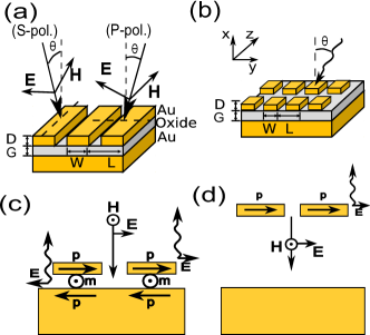
In the following we concentrate on the specific geometry of a resonant plasmonic absorber schematically shown in Fig. 1(a,b), which is comprised of a periodic array of either plasmonic strips or square patches separated from a thick (non-transparent) plasmonic mirror (further referred to as the ground plate following the standard microwave terminology). As shown in Section IV, the spectral response of the square-patch structure shown in Fig. 1(b) is qualitatively (and even quantitatively) similar to that of the one-dimensional structure. In this section we concentrate on the one-dimensional array of plasmonic strips Wu et al. (2008) shown in Fig. 1(a), where all dimensions of the plasmonic absorber are defined. The structure is assumed uniform in the -direction and repeating in the -direction with periodicity . Below we develop the theoretical formalism for computing the absorption of the nano-structured plasmonic surface based on the eigenvalue/eigenmode analysis. For simplicity, we restrict the incident wave to be P-polarized as shown in Fig. 1(a), i.e., the incident wavenumber and the electric field lie in the - plane, whereas the magnetic field is aligned in the -direction.
In earlier reports on MM absorbers, the perfect absorption was explained in terms of matching the bulk metamaterial’s impedance to that of vacuum Avitzour et al. (2009b); Liu et al. (2010b); Landy et al. (2008b, 2009), where and are the effective permittivity and permeability of the bulk multi-layer (i.e., stacked in the vertical -direction) metamaterial. Typically, these effective constitutive parameters are obtained from the scattering matrices of either a single layer or multiple layers of the MMs Smith et al. (2002) under the assumption of homogeneous media. To satisfy the condition of matched impedances, the condition of (which are both, in general, complex numbers) is achieved Avitzour et al. (2009b) by manipulating the spectral positions and strengths of the electric and magnetic resonances of the MMs. However, this viewpoint is not appropriate for MMs using a thick ground plate because the S-matrix is not fully defined when transmittance vanishes. Additionally, the ambiguity in the MM thickness also poses a problem in calculating and .
Here we explain the phenomenon of perfect absorption in terms of critical coupling to the MM surface. This perspective is more adequate for our situation with blocked transmission. It provides a guideline on how the structure should be designed, and also reveals the persistence of high absorbance over structural variation. Critical coupling occurs when a leaky eigenmode of the structure has equal resistive and radiative losses. For a critically coupled MM, an incoming field excites the eigenmode through radiative coupling, and the incoming energy transforms into resistive loss without generating reflection. Therefore, a MM absorber with blocked transmission is analogous to the single resonator coupled to a single input waveguide. This problem has been well-studied Haus (1984), and the reflection coefficient can be expressed as a function of the resonant frequency, , the radiative damping/coupling rate, , and the resistive damping rate, , of the resonator. The impedance of the MM surface defined as is given by:
| (1) |
From Eq. (1), the critical coupling condition is satisfied when . Because the ground plate transmits no light, the absorptivity of the structure , which is determined by its reflectivity according to , reaches unity at . Note that diverges at the complex frequency if , or , where . Because the divergence of the reflectivity corresponds to the eigenmode of the “leaky” resonator (or, in our case, leaky plasmonic absorber), we can calculate by computing the complex eigenfrequency of the absorber. The corresponding plasmonic eigenmode is further used to break up the total decay rate into the Ohmic (resistive) and radiative parts. A similar approach Neuner III et al. (2009) was recently used to describe critical coupling to surface polaritons excited in the Otto configuration.
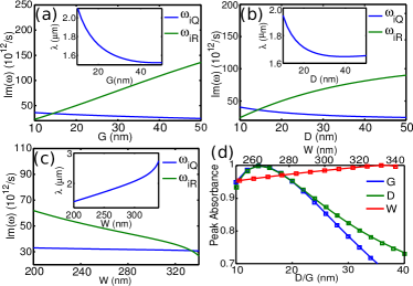
The calculation was performed using the finite element method (FEM) software COMSOL Multiphysics. A single unit cell was modeled; periodic boundary conditions (BCs) in the -direction (corresponding to the normal incidence) and radiative BCs in the -direction were assumed in the simulation. The magnetic field distribution (color) and electric field vectors (arrows) of the most dominant magnetic resonance mode is shown in Fig. 4(b). Both the strips and the ground plate are gold with dielectric permittivity given by the Drude model Dolling et al. (2006): , where and . By computing the Ohmic losses and the power out-flux proportional to the Poynting vector, we have calculated and . These quantities were used in computing the resistive and radiative damping rates and , respectively, which are required for calculating from Eq. (1). The dependence of and on the geometric parameters of the absorber are shown in Fig. 2.
According to Fig. 2(a), the radiative loss associated with the eigenmode dominates over the resistive loss whenever plasmonic strips are separated from the ground plate by a large distance . Therefore, of an external beam tuned to ( is plotted in the inset) is large, and the absorbance is small, which is not surprising because the ground plate is highly reflective. On the other hand, if the strips are close to the plate, a strong image dipole moment is generated behind the ground plate as shown in Fig. 1(b). The resulting strong magnetic moment directed along the strips produces back-scattered fields with phase opposite to those produced by the reflection from the ground plate. Such destructive interference reduces the total backward scattering. With a suitable choice of , critical coupling can be achieved when the scattering cross-section becomes equivalent to the resistive cross-section. Such cancellation does not occur for large s because electric field is mostly concentrated between the adjacent strips, not between the strips and the ground plate. Therefore, the magnetic moment is too weak to significantly reduce ground plate reflection. Other geometric parameters also affect the total radiative loss. For a fixed periodicity nm, we observe from Fig. 2 that radiative loss can be decreased by increasing the strip width or decreasing the strip thickness .
Assuming the single dominant resonance of the absorber, the peak reflectivity at the resonant frequency can be recast as
| (2) |
confirming that “perfect” peak absorption is achieved if . The peak absorbance obtained from Eq. (2) is plotted in Fig. 2(d) (markers) and compared with the peak absorbance obtained from driven simulations (solid lines) for varying structure parameters. Excellent agreement is found between the single-pole impedance approach based on eigenvalue simulations and the driven simulations that include incident waves with frequencies scanned over a wide spectral range. The advantage of the eigenvalue-based approach is that only a single simulation is required to compute and, therefore, the peak absorbance. A full frequency scan (i.e., multiple FEM simulations) is needed to find the peak absorbance using driven simulations.
One interesting consequence of Eq. (2) is that the absorbance can still be large even when the radiative loss is considerably mismatched from the resistive loss. For example, when , the absorbance still reaches 96. We refer to this phenomenon as the persistence of high absorptivity despite considerable variations of the absorber’s parameters. This insensitivity to the strip width , strip thickness , and strip-to-ground plate spacing is shown in Fig. 2(d): the absorbance stays above despite considerable variation (by as much as a factor ) of these parameters.
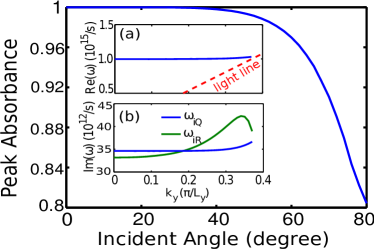
To investigate the angular response of the plasmonic absorber, we have computed eigenmodes and eigenfrequencies of “leaky” surface plasmons propagating along the periodicity direction with a finite wavenumber . As long as , such plasmons are “leaky” because they can directly couple to the radiation with the frequency incident at the angle with respect to the (normal) -direction. Therefore, they can be responsible for wide-angle absorption of the obliquely incident radiation. Just as for the normal incidence, one expects critical coupling and “perfect” absorption when . Indeed, as Fig. 3 indicates, the two damping rates are very close to each other. Moreover, the resonant wavelength remains essentially flat for all values of . The consequence of a flat response is persistently high absorbance (between and ) of the plasmonic structure as the incidence angle is varied in the range. In Section IV, we present experimental confirmation of wide-angle absorption.
III Fabrication of the absorber
In this section we provide a detailed technical description of the fabrication procedure of the Large Area Wide-Angle Spectrally Selective Plasmonic Absorber (LAWASSPA). The structure was fabricated using nano-imprint lithography Chou et al. (1996); Johnson et al. (2003), which provides a means to create many replicate copies of devices via pattern transfer from a quartz master template that is initially defined using electron beam lithography (EBL). Once the EBL pattern is etched into quartz, the patterned quartz template is used to stamp photoresist layers under UV exposure (i.e., a step-and-flash process). Release of the quartz template leaves the desired relief pattern on the wafer surface. Subsequent dry etching transfers the pattern into the desired layer, which are thin gold strips in this work. The feature dimensions are limited only by the resolution of the initial electron beam process, which is 50 nm for the JEOL JBX6000 EBL tool at the University of Texas at Austin’s Microelectronic Research Center (MRC). For volume production, resolution can be as low as 20 nm imp .

To fabricate the devices, Cr-Au-Cr layers (3 nm-94 nm-3 nm) were deposited on a 4" silicon
wafer by electron beam evaporation. A layer of In2O3 (20 nm) followed by SiO2 (1 nm) were
deposited by PECVD as the dielectric spacer. An additional Cr-Au layer (3 nm-30 nm) was
subsequently deposited on the dielectric spacer. Nano-imprint lithography is used to pattern the
top Cr-Au layer into metal strips, which begins by spin-coating a layer of . A
number of combinations of metal strip width (100-300 nm) and pitch (175-450 nm) were
patterned into the quartz template as 1.4 mm2 islands, providing a range of peak absorbance
wavelengths to investigate.
Nano-imprint lithography begins by dispensing curable liquid (silicon-based ) with high precision over the desired area. The quartz master is pressed against the surface of the wafer (feature side down) and the flows to fill the relief pattern in the quartz. Ultraviolet exposure sets the and the quartz master is released from the surface leaving the imprinted pattern. After release, the residual layer is dry etched by reactive ion etching (Oxford RIE, 200 V DC bias, 15 sccm CHF3, 7.5 sccm O2, 25 mtorr) followed by dry etching of the layer (200 V DC bias, 8 sccm O2, 5 mtorr). The pattern is transferred into the Au/Cr layer using a physical reactive ion etch in Ar (250 W, 50 sccm Ar, 40 mtorr). A final O2 plasma etch (March Asher) was used to remove remaining and , yielding the final device structure. An representative SEM image of the structure with =300 nm and =230 nm is shown in Fig. 4(a). A single wafer contains a large number of LAWASSPA pixels with different unit cell sizes. Each pixel has the size of approximately 1 mm2, and is tuned to a different resonant wavelength determined by the unit cell’s dimensions and .
IV Angle-resolved Infrared Spectroscopy of Wide-Angle Plasmonic Absorbers
In this section, we experimentally demonstrate that (i) the absorption peak of the infrared plasmonic resonance can be spectrally tuned/controlled by changing the unit cell’s dimensions as described in Sec. II, and (ii) that the absorbance is wide-angle in agreement with earlier theoretical calculations Wu et al. (2008); Diem et al. (2009); Liu et al. (2010a); Hao et al. (2010) and with the theory presented in Sec. II. To test (i), we have measured the reflection spectra from different LAWASSPA pixels fabricated on a single wafer as described in Sec. III. Reflectance () spectra were collected with a Thermo Scientific Continuum microscope coupled to a Nicolet 6700 FTIR spectrometer using P-polarized radiation and a 2 cm-1 wavenumber resolution in the 7000 cm-1–650 cm-1 (1.4 m–15.4 m) spectral range. A wire-grid polarizer aligned the electric field polarization along the periodicity direction as illustrated by Fig. 4(b).
Experimental absorbance for several LAWASSPA pixels of different dimensions are shown in Fig. 4(c) by solid lines for the -polarized infrared radiation. The incidence angle of the infrared beam on the sample is approximately fixed at by microscope optics. By changing the unit cell’s dimensions and (see Fig. 1 for definitions), we have experimentally demonstrated spectral tunability of the plasmonic absorber between m and m for the -polarized beam. Much smaller absorption measured for the orthogonal light polarization (electric field parallel to the long dimension of the strips) shown in Fig. 4(c) by the dashed lines does not exhibit any spectral selectivity. As expected, the strip-based plasmonic absorber is polarization-sensitive: it acts as a “perfect” absorber/reflector for the /-polarized beams.
Simulations were performed and compared with experimental results. In calculations, the Drude model for Au and the refractive index for In2O3 were used. Theoretical absorption spectra plotted in Fig. 4(d) for the same unit cell dimensions as the fabricated samples (solid lines) show good agreement with the experimental spectra plotted in Fig. 4(c). To account for thin post-etching metal residue between the strips that was identified in SEM images, an extra 2 nm of Au on top of the spacer was assumed in calculations. The effect of this metal residue is a slight blue-shifting of the resonance. While the extra metal layer was not intentional in this set of experiments, it could become a useful feature for specific applications that require electric contact between the metal strips of the absorber.
Likewise, polarization selectivity of strip-based plasmonic absorbers could be useful for some applications (e.g., thermal infrared emitters with controlled polarization state) and detrimental for others (e.g., infrared photodetectors). Nevertheless, the results obtained for the strip-based absorbers are directly relevant to patch-based Liu et al. (2010a); Hao et al. (2010) polarization-insensitive absorbers shown in Fig. 1(b). Specifically, using COMSOL simulations, we have found that the absorptivity of an array of square patches is essentially identical to that of the infinite strips if the widths and periods ( and ) of these structures are chosen to be identical. The comparison between strip-based (solid lines) and patch-based (dotted lines) plotted in Fig. 4(d) shows only a small systematic red shift of the latter with respect to the former. This observation is useful from the design standpoint because strip-based absorbers are much easier to simulate using two-dimensional FEM simulations. Strip-based absorbers provide an excellent starting point for designing fully three-dimensional patch-based plasmonic absorbers. We conclude that, while 2D strip arrays are easier to analyze and engineer, absorbers with both strip and square patch arrays show the same physics of critical coupling and high absorbance if their geometric parameters are near-identical.

If the structure is to be used as an effective absorber, the absorption rate must remain high for a wide range of incident angles. Because the spectra shown in Fig. 4(c) were obtained using a fixed-angle geometry (IR microscope), a separate optical setup enabling variable-angle spectroscopy was used to test the wide-angle properties of the absorber. The beamline is based on the FTIR spectrometer and uses standard infrared focusing optics assembled on the optical table. It provides a means for variable incidence angles, polarization control, and a 200-m spot size. The geometric parameters of the strip-based LAWASSPA are given by [,,,]=[300 nm, 230 nm, 10 nm, 17 nm], and the dielectric spacer is SiO2 (). Angle-resolved absorption spectra were measured for both S and P polarizations of the incident light as illustrated in Fig. 1(a), and presented as a color map in Figs. 5(a) and (b), respectively.
Both polarizations exhibit a fairly wide-angle absorptivity, although P polarization is much less angle-dependent than S polarization. As was noted in earlier theoretical work Wu et al. (2008), this dependence occurs because the plasmonic resonance responsible for “perfect” absorption is primarily magnetic and, therefore, is sensitive to the out-of-plane component of the magnetic field. The qualitative agreement between theory (Fig. 5(c,d)) and experiment (Fig. 5(a,b)) is excellent. Inhomogeneous broadening of the experimental spectra compared to theoretical predictions most likely results from the absorber’s structural imperfections. However, as we have demonstrated, the absorber design is robust against imperfections, and therefor the absorptivity remains high. One unintentional but interesting feature of this absorber is that the absorption is not maximized at normal incidence. In fact, for P polarization, the measured absorbance peaks at for and drops to for .
V Design of Small-Pixel Infrared Absorbers
In this section, we discuss the implications of the wide-angle absorptivity of the infrared plasmonic absorbers. One of the consequences of wide-angle absorptivity is that the coherence propagation length of the surface plasmon responsible for the absorption is very short. If , then the interaction between the adjacent unit cells is small. Therefore, one can envision combining a very small number of unit cells into a micro-pixel which can be as small as one wavelength across. Such micro-pixels can act as an independent absorber/emitter. One possible application of such micro-pixels could be a large focal plane array (FPA) for hyper-spectral imaging. Such an array would consist of macro-pixels comprised of several micro-pixels, each of which is tuned to a different wavelength. For example, a macro-pixel comprised of a micro-pixels of width (where ) would be capable of monitoring 25 different wavelengths while remaining relatively small. The small size (several wavelengths across) of a macro-pixel is essential for imaging/surveillance with a small angular resolution.
Our experimental data indeed indicates that and, therefore, the adjacent unit cell have very little cross-talk between them. Quantitative estimate of the propagation length can be obtained from the angular dependence of the absorptivity which is plotted in Fig. 5 as a function of the related variables and . The propagation length along the -direction is given by , where is the group velocity in the -direction, and is the lifetime of the resonant mode that can be estimated as . Assuming that the absorption rate is maximized at the angle-dependent eigenfrequency , and that the peak absorption rate remains close to unity (), we find that . Combining these expressions for and , and by assuming that , we obtain the following simple estimate for the propagation length: . By noting that , we estimate the maximum plasmon propagation length as . From the experimental data for the wide-angle absorber, we estimate that the propagation length cannot exceed nm, i.e., about one period. Therefore, a resonant mode in a single cell is significantly damped before reaching adjacent unit cells, and the cross-talk between them is small.
To substantiate our claim that the unit cells of the MM absorber function independently, the absorbance of a limited number of MM unit cells is investigated theoretically. In Fig. 6, we consider an incoming Gaussian beam with an intensity FWHM of 2.6 m impinging on MM surfaces consisting of 4, 8, 12, and 16 unit cells. The unit cells possess [,,,]=[350 nm, 250 nm, 20 nm, 14 nm]. The metal is Au and the spacer is SiO2. Figure 6(a) shows absorbance with different numbers of unit cells, whereas in Fig. 6(b) the peak absorbance is compared to the incoming flux within the structured area. It is shown from the comparison that the MM absorber remains perfect absorbing to the incident flux, even though the incoming field is not planar and the MM consists of as few as four unit cells. This property can find applications in thermal imaging, where a pixel can be defined by a small number of MM unit cells. On-chip spectrometers are also envisioned, in which MM absorbers tuned to different wavelengths are patterned side-by-side on a single chip.

VI Conclusions
In conclusion, we have demonstrated a simple design of an ultra-thin, wide-angle plasmonic absorber exhibiting spectrally selective near-unity absorption. The high absorbance of the structure is described in terms of critical coupling, where the scattering cross-section is equal to the absorptive cross-section. The critical coupling perspective provides a guideline for designing MM absorbers with tunable resonant frequencies: with low loss metals, the structure should be designed in such a way that the resonances have low radiative loss. Based on this theory, the gold strips and ground plate in this simple structure can be replaced by other metals, e.g., tungsten for high-temperature applications, and the dielectric spacer layers can be replaced by absorbing materials, e.g., semiconducting materials for photovoltaic applications. We have also developed a convenient tool for designing such structures based on the eigenvalue simulations of the “leaky” plasmon resonances. These simulations are used for calculating the impedance of the absorbing surface at arbitrary frequencies, which can then be used for predicting absorbance and reflectance.
Because a number of applications require inexpensive, large-area plasmonic absorbers, the fabrication approach is paramount. We have fabricated plasmonic absorbers using step-and-flash ultraviolet nano-imprint lithography, which has the advantages of reusable masks and large-area fabrication compared with the serial fabrication methods. By patterning absorber pixels of various dimensions over a large area, we have experimentally demonstrated that the spectral response of the absorber can be controlled over a wide wavelength range (m m) while maintaining a near-unity peak absorbance. Using angle-resolved infrared spectroscopy, we have experimentally demonstrated that these Large-Area, Wide-Angle, Spectrally Selective Plasmonic Absorbers (LAWASSPA) exhibit near-unity absorptivity for incidence angles from to . Moreover, we have experimentally demonstrated and theoretically validated that P-polarized light exhibits wider-angle absorption than S-polarized light. Such wide-angle absorption indicates short propagation lengths (less than one unit period) of the plasmonic mode, a feature useful in designing ultra-small (one wavelength across) absorbing pixels that can be used as building blocks for hyper-spectral focal plane arrays and infrared emitters.
VII Acknowledgments
This work is supported by the Office of Naval Research (ONR) grant N00014-10-1-0929 and ONR’s STTR program.
References
- Veselago (1968) V. G. Veselago, Soviet Physics Uspekhi 10, 509 (1968).
- Smith et al. (2000) D. R. Smith, W. J. Padilla, D. C. Vier, S. C. Nemat-Nasser, and S. Schultz, Phys. Rev. Lett. 84, 4184 (2000).
- Pendry (2000) J. B. Pendry, Phys. Rev. Lett. 85, 3966 (2000).
- Schurig et al. (2006) D. Schurig, J. J. Mock, B. J. Justice, S. A. Cummer, J. B. Pendry, A. F. Starr, and D. R. Smith, Science 314, 977 (2006).
- Alu and Engheta (2004) A. Alu and N. Engheta, IEEE Trans. Microw. Th. Tech. 52, 199 (2004).
- Chen et al. (2008) H.-T. Chen, J. F. O’Hara, A. K. Azad, A. J. Taylor, R. D. Averitt, D. B. Shrekenhamer, and W. J. Padilla, Nature Photon. 2, 295 (2008).
- Landy et al. (2008a) N. I. Landy, S. Sajuyigbe, J. J. Mock, D. R. Smith, and W. J. Padilla, Phys. Rev. Lett. 100, 207402 (2008a).
- Coutts (1999) T. J. Coutts, Renewable and Sustainable Energy Rev. 3, 77 (1999).
- Laroche et al. (2006) M. Laroche, R. Carminati, and J. J. Greffet, J. Appl. Phys. 100, 063704 (2006).
- Tvingstedt et al. (2007) K. Tvingstedt, N. K. Persson, O. Inganas, A. Rahachou, and I. V. Zozoulenko, Appl. Phys. Lett. 91, 113514 (2007).
- Avitzour et al. (2009a) Y. Avitzour, Y. A. Urzhumov, and G. Shvets, Phys. Rev. B 79, 045131 (2009a).
- Wu et al. (2008) C. Wu, Y. Avitzour, and G. Shvets, Proc. SPIE 7029, 70290W (2008).
- Diem et al. (2009) M. Diem, T. Koschny, and C. M. Soukoulis, Phys. Rev. B 79, 033101 (2009).
- Hao et al. (2010) J. Hao, J. Wang, X. Liu, W. J. Padilla, L. Zhou, and M. Qiu, Appl. Phys. Lett. 96, 251104 (2010).
- Liu et al. (2010a) N. Liu, M. Mesch, T. Weiss, M. Hentschel, and H. Giessen, Nano Letters 10, 2342 (2010a).
- Tao et al. (2008) H. Tao, C. M. Bingham, A. C. Strikwerda, D. Pilon, D. Shrekenhamer, N. I. Landy, K. Fan, X. Zhang, W. J. Padilla, and R. D. Averitt, Phys. Rev. B 78, 241103(R) (2008).
- Urzhumov and Shvets (2008) Y. Urzhumov and G. Shvets, Solid State Comm. 146, 208 (2008).
- Johnson et al. (2003) S. Johnson, T. Bailey, M. Dickey, B. Smith, E. Kim, D. Mancini, W. Dauksher, K. Nordquist, and D. Resnick, Proc. SPIE 5037, 197 (2003).
- Avitzour et al. (2009b) Y. Avitzour, Y. A. Urzhumov, and G. Shvets, Phys. Rev. B 79, 045131 (2009b).
- Liu et al. (2010b) X. Liu, T. Starr, A. F. Starr, and W. J. Padilla, Phys. Rev. Lett. 104, 207403 (2010b).
- Landy et al. (2008b) N. I. Landy, S. Sajuyigbe, J. J. Mock, D. R. Smith, and W. J. Padilla, Phys. Rev. Lett. 100, 207402 (2008b).
- Landy et al. (2009) N. I. Landy, C. M. Bingham, T. Tyler, N. Jokerst, D. R. Smith, and W. J. Padilla, Phys. Rev. B 79, 125104 (2009).
- Smith et al. (2002) D. R. Smith, S. Schultz, P. Markos, and C. M. Soukoulis, Phys. Rev. B 65, 195104 (2002).
- Haus (1984) H. A. Haus, Waves and Fields in Optoelectronics (Prentice-Hall, 1984).
- Neuner III et al. (2009) B. Neuner III, D. Korobkin, C. Fietz, D. Carole, G. Ferro, and G. Shvets, Opt. Lett. 34, 2667 (2009).
- Dolling et al. (2006) G. Dolling, C. Enkrich, M. Wegener, C. M. Soukoulis, and S. Linden, Science 312, 892 (2006).
- Chou et al. (1996) S. Y. Chou, P. R. Krauss, and P. J. Renstrom, J. Vac. Sci. Technol. B 14, 4129 (1996).
- (28) http://www.molecularimprints.com.