Also at ]St. Petersburg Academic University of the RAS, Khlopina 8/3, 195220 St. Petersburg, Russia Also at ]St. Petersburg Academic University of the RAS, Khlopina 8/3, 195220 St. Petersburg, Russia Also at ]St. Petersburg Academic University of the RAS, Khlopina 8/3, 195220 St. Petersburg, Russia Also at ]St. Petersburg Academic University of the RAS, Khlopina 8/3, 195220 St. Petersburg, Russia
Optical Study of GaAs quantum dots embedded into AlGaAs nanowires.
Abstract
We report on the photoluminescence characterization of GaAs quantum dots embedded into AlGaAs nano-wires. Time integrated and time resolved photoluminescence measurements from both an array and a single quantum dot/nano-wire are reported. The influence of the diameter sizes distribution is evidenced in the optical spectroscopy data together with the presence of various crystalline phases in the AlGaAs nanowires.
pacs:
61.46.Km, 78.55.Cr, 78.47.jd, 68.37.Hk, 68.37.LpIntroduction
Free-standing semiconductor nanowires (NWs) are promising one-dimensional nanostructures for applications in nanoelectronics [Bryllert et al. (2006)], and nanophotonics [Gradecak et al. (2005)], as well as for fundamental research [Schubert et al. (2004); Seifert et al. (2004); Dubrovskii et al. (2005); Harmand et al. (2005); Plante and LaPierre (2006); Dubrovskii et al. (2006)]. The technology of fabrication of such NWs is developing intensively nowadays [Glas and Harmand (2006); Persson et al. (2009); Gudiksen et al. (2002); Bjrk et al. (2002); Cui and Lieber (2000); Patolsky et al. (2004)]. Recently, an opportunity has been demonstrated to embed one or several quantum dots into NW. Modern epitaxial techniques enable one in principle to control the sizes and positions of NW at the nanometer scale, which is very attractive for applications. The important task for today in this area is to obtain highly homogenous ensembles of NWs that have a small distribution of sizes and well-determined spatial positions, in order to use them in nanoelectronics. Despite very impressive progresses in nanowire fabrication, many growth-related aspects in this field are not completely understood so far. In particular, it is very important to determine the growth procedure (temperature, flow rates etc) that allows one to produce homogenous NWs ensembles.
I Experiment
In these studies we used AlGaAs nanowires (NWs) with embedded GaAs quantum dots (QDs). AlGaAs NWs were grown on GaAs (111)B semi-insulating substrate using EP1203 MBE system equipped with solid sources supplying Ga and Al atoms, and an As effusion cell to produce tetramers. The substrate surface was first deoxidized at 630oC, then a 100 nm thick GaAs buffer layer was grown at 600oC to achieve an atomically-flat surface. A total amount of Au equivalent to 1 nm layer was deposited without V-group flux at 550oC using an Au effusion cell installed directly into the III-V growth chamber followed by a 1 min waiting time to achieve better homogeneity of the droplets. The substrate temperature was then set to the desired value for the growth (550oC or 580oC). This procedure induces the formation of droplets containing Au alloyed with the substrate constituents. The typical distribution of droplet sizes ranges between 40 nm and 50 nm. The NW growth was initiated by opening simultaneously the Al, Ga and As sources. For the samples the nominal growth rates, i.e. the growth rate on a clean and Au-free surface, were fixed at 1 monolayer (ML)/s for GaAs and AlAs 0.4 ML/s. The resulting AlxGa1-xAs growth rate was 1.4 ML/s corresponding to an Al content in the solid solution of = 0.285 for a planar layer. As the Al content in the NW and planar layer could be not the same, the NW composition was measured especially by Raman spectroscopy. We have found that in our NWs = 0.24 – 0.26.
For AlGaAs/GaAs/AlGaAs quantum dot formation, the growth started with 15 min of AlGaAs, and then the Al source was closed for 5 sec in order to form a GaAs slice in each NW. Then, the growth of AlGaAs was performed again to produce a core – shell structure. The growth was completed with 2 min deposition of GaAs at 530oC to avoid possible oxidation of AlGaAs shell layer. We did not perform any growth interruption at the heterointerfaces. The diameter of NWs in our samples was 30-60 nm. Scanning electron microscopy (SEM) and transmission electron microscopy (TEM) characterizations were performed before the optical measurements.
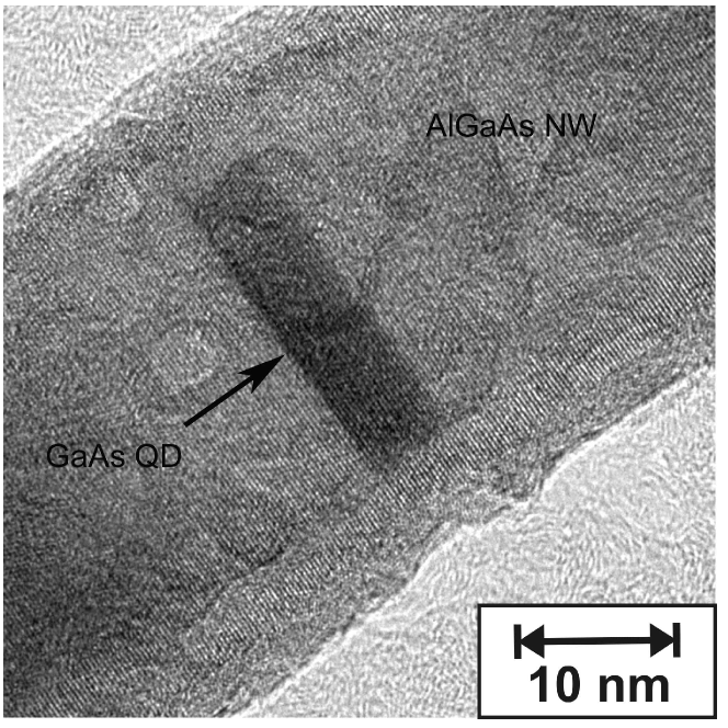
The TEM image of the single AlGaAs NW with a slice of GaAs is shown in Fig. 1. The dark area on the image in the center of the single NW corresponds to the single GaAs QD. It is clearly seen that the interfaces along the axis of growth and along the radius are rather sharp. The GaAs QD looks like a disk surrounded by wide-gap semiconductor AlGaAs. The diameter of the NW in our samples was 25-50 nm, the length 500 nm, and the thickness of the QD was of several mono-atomic layers i.e. 2-5 nm.
A systematic steady state and time resolved photoluminescence (PL) study was performed on a set of samples in the temperature range from 5 K up to 250 K and for various optical excitation densities. The samples were excited by either second harmonic of Nd:YAG laser or doubled Ti:Sa laser with 100 fs pulse duration. Jobin-Yvon 30 cm monochromator and avalanche photodiode were used for registration.
II Results
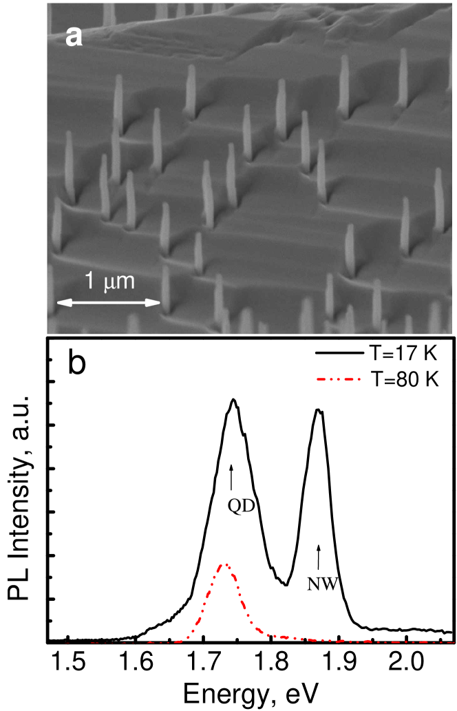
Figure.2a shows an SEM image of the sample grown at ”high” temperature (580oC). It is seen that the nano-wires are strongly inhomogeneous in diameters and positions on the substrate.
The diameter dispersion ranges between 100 Å and 500 Å, and can even change along a given wire. Most of the wires are perpendicular to the substrate, but some of them are lying horizontally, revealing also the orientations inhomogeneity and some of them are cut from the substrate at all. It is clear that this sample is strongly inhomogeneous.
Photoluminescence spectrum from this type of sample is shown on Fig.2b The spectrum is very broad and spreads from 1.65 eV to 1.95 eV without any reproducible structure. This emission band is a mixture of recombination coming from NWs and QDs embedded into them, without any possibility to separate both contributions.
Instead, for samples grown at lower temperature (550oC), a much better homogeneity is obtained for both the diameters and the length of the NWs (see Fig.3a). For example, we can estimate from this figure that the distribution of the NW diameters does not exceed 15 %. Additionally, the diameter does not change along the wire.

b. Photoluminescence spectrum taken from the given sample.
The PL spectrum taken from this structure at temperature of 10 K is presented in Fig.3b by solid line. Two intense lines at energies 1.73 eV and 1.87 eV are dominate in the spectrum. These lines are attributed to carrier recombination respectively in the quantum dots and in the nanowires.
Indeed, the nano-wire material AlxGa1-xAs, has bandgap =1.8 - 1.9 eV, and the bandgap of the quantum dot material is =1.519 eV at helium temperatures. Consequently, the PL line of quantum dots can has energies from =1.519 eV, in very large dots to =1.8 eV, in very small dots. From the other hand the PL line of NW can not be lower in energy than the Al0.25Ga0.75As bandgap, i.e. can not be below =1.8 eV. By contrast with the results shown on figure 2b, the width of these PL lines reveals a much narrower distribution of NW diameters, which do not exceed 15%.
b. Photoluminescence spectra taken at two temperatures for the given sample .
The difference in the nature of these two lines shown in figure 3b is confirmed by the temperature dependence of the emission spectrum. The PL spectrum taken at 77K is presented in Fig.3b by the dashed line: the intensity of the nano-wire line completely disappears with temperature, whereas the one of the QD line drops down by only a factor three. This evidences the strong localization of the carriers at the origin of the QD line, by contrast to the one in the recombination of the line at higher energy (1.87 eV) which can diffuse along the wire axis and be capture by the QD.
Comparing the results shown in Fig.2 and Fig.3 we can conclude that it is possible to obtain a homogenous distribution of NW diameters by adjusting the growth conditions.
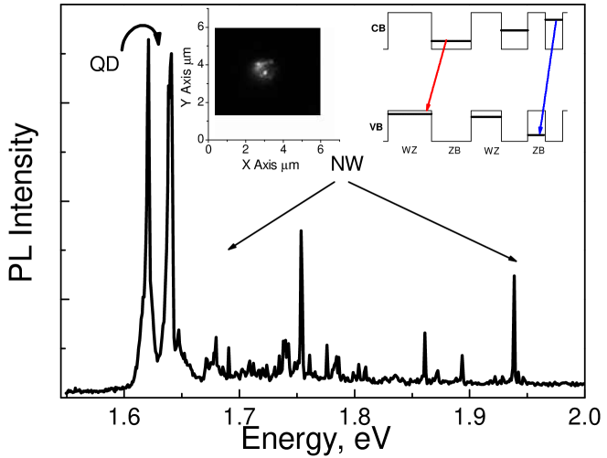
Left inset: Spatially resolved PL of the area under study.
Right inset: The scheme of the effective type-II ”superlattice” formation.
Having optimized the growth process to obtain a homogeneous distribution of NW diameters, we performed an optical study (PL spectra and time resolved spectroscopy) on a single QD and single NW. For this purpose a strongly increased image of the sample surface was projected into the slit of the spectrometer. As a result, only the signal coming from a very small number of NWs is collected. The spatial resolution of the objective was 1.5 micron, and the average distance between nano-wires was about 0.8 microns. Consequently the photodetector can collect a signal coming from several nano-wires contained quantum dots of little different sizes. Spatially resolved PL image is shown in the right insert to Fig.4a. In the present case, the emission spectrum shown on Fig.4a, corresponds to three NWs having a diameter nearly 50 A bigger than the one of the sample presented in Fig.3. There are two groups of lines in this spectrum: three relatively wide lines in the energy range 1.6 – 1.65 eV and many irregular distributed narrow lines at higher energy (1.75 – 1.95 eV).

The line at 1.62 eV and the doublet at 1.64 eV are attributed to the PL from the three single quantum dots embedded in the NWs. Such interpretation is confirmed by time resolve PL measurements, as shown in Fig.5. The decay time for all these three lines was found to be the same and equal to 5 nsec. This is a little bit longer than the value obtained for the decay time of the exciton recombination in self-assembled (Stranski - Krastanov) quantum dots, but is remarkably shorter than the decay time obtained for all other lines (20 nsec) in this spectrum.
The full width at half maximum (FWHM) of the emission line of a single quantum dot was found to be relatively large (typically 0.2 meV). Such linewidth is not lifetime limited; it implies instead that the linewidth is not an intrinsic property of genuine quantum dots, but a consequence of their local environment, which can be explained by fluctuating Stark shift caused by photo-excited charged carriers. Such results were already reported Kuroda et al. (2007) for lattice matched quantum dots like GaAs/AlGaAs by using a droplet epitaxy method.
The origin of the linewidth could be due also to the centre of mass quantization of the exciton in the transverse direction of the NW: indeed, quantum dots in our samples have a disk shape, with thickness of about 20 – 50 Å and diameter of 200 – 500 Å. The electron quantization energy in such disks is tens and even hundreds meV for quantization along the NW axis, but nearly one hundred times less for ”transverse” quantization. As a result the energy levels of the transverse quantization will concentrate in the vicinity of the main level of the longitudinal quantization. The lines of allowed optical transitions in this case will look as an array of narrow lines of smaller intensity concentrating around the main line.
At high enough optical excitation all these closely situated levels are populated by carriers. This leads to the large observed line-width and to the increasing of the PL decay time up to 5 nsec. Unfortunately it was not possible in our experiments to decrease the excitation density at a value small enough without loosing the signal detected by the system. However, by increasing the photoexcitation power, these lines become broader.
Then all the optical data for the low energy lines are consistent with the emission coming from highly populated quantum dots in the NWs.
Concerning the array of irregular distributed lines at higher energies (1.75 eV – 1.95 eV), there are attributed to carriers recombination in single nano-wires. As it was mention before, the effective bandgap of the nano-wire can not be smaller the bandgap of bulk AlGaAs – the material in which the nano-wire made. However, in our spectrum (Fig. 4a) the line at 1.75 eV is at about 50 meV less than the bandgap energy of the AlGaAs with x = 25%. The decay time of the PL for this line is long - 20 nsec, and it disappears at temperature of 77 K which is typical for a PL signal coming from carriers in the NW.
We suppose that the appearance of these lines are connected with spontaneous formation of mix phase (wurtzite)-(zinc blend).
The observation of such lines in the range 1.75 – 1.95 eV with an irregular distribution can be explained taking into account the effect of the crystalline phase transition which is known to exist in such nano-wires [Shtrikman et al. (2009); Dubrovskii et al. (2009); Spirkoska et al. (2009)]. Namely in the AlGaAs nano-wire the crystalline structure can switch spontaneously from the zinc-blende (ZB) to the hexagonal wurtzite (WZ) structure. Since there is a difference for the band gap for ZB and WZ AlGaAs, the alternation in crystalline structure leads to the formation of an effective type-II ”superlattice” along the growth direction (see the left insert of Fig4a) inducing a quantization of the carriers along the growth axis. Consequently, the spectrum of the carriers is transformed into a quasi-zero-dimensional one rather than a one-dimensional one specific to the homogenous wire. It is clear that the quantization energy depends on the thickness of the layers with the same crystalline structure. Since the thickness was an uncontrolled parameter in our setup we obtain a random distribution of the carrier energy states as illustrated on the left insert of Fig. 4a).
The long decay time, typically 20 nsec) for all these lines in the range from 1.75 eV – 1.95 eV confirms such interpretation, namely these lines are related to the spatially indirect recombination in type-II structures.
III Conclusion
Photoluminescence spectra from the QD embedded into NW have been measured. It has been shown that by adjusting growth procedure one can obtain a homogenous distribution for the QD/NW sizes. The micro-PL spectroscopy reveals the carriers recombination both into the QDs and into the NWs. For the first one FWHM and decay times values appear to be larger than the one obtained in self-assembled QDs which could be due to not only some spectral diffusion but also to some influence of the transverse quantization. As far as the second are concerned there are attributed to recombination between electrons in the ZB AlGaAs layers and holes in the WZ AlGaAs layers. The long decays obtained for these latter transitions strongly support such interpretation on the formation of type II superlattice between ZB and WZ phases.
Acknowledgements.
This work was supported in part by grants of Presidium RAS, the Russian Federal Agency for Science and Innovation (Contract No. 02.740.11.0383), different RFBR grants and the program of cooperation between RFBR and CNRS.References
- Bryllert et al. (2006) T. Bryllert, L. E. Wernersson, T. Lowgren, and L. Samuelson, Nanotechnology 17, S227 (2006).
- Gradecak et al. (2005) S. Gradecak, F. Qian, Y. Li, H. G. Park, and C. M. Lieber, Appl. Phys. Lett. 87, 173111 (2005).
- Schubert et al. (2004) L. Schubert, P. Werner, N. Zakharov, G. Gerth, F. Kolb, L. Long, U. Gsele, and T. Tan, Appl. Phys. Lett. 84, 4968 (2004).
- Seifert et al. (2004) W. Seifert, M. Borgstrom, K. Deppert, K. Dick, J. Johansson, M. Larsson, T. Martensson, N. Skold, C. Svensson, B. Wacaser, L. Wallenberg, and L. Samuelson, J.Cryst. Growth 272, 211 (2004).
- Dubrovskii et al. (2005) V. Dubrovskii, G. Cirlin, I. Soshnikov, A. Tonkikh, N. Sibirev, Y. Samsonenko, and V. Ustinov, Phys. Rev. B 71, 205325 (2005).
- Harmand et al. (2005) J. C. Harmand, G. Patriarche, N. Péré-Laperne, M.-N.Mérat-Combes, L. Travers, and F. Glas, Appl. Phys. Lett. 87, 203101 (2005).
- Plante and LaPierre (2006) M. C. Plante and R. R. LaPierre, J. Cryst. Growth 286, 394 (2006).
- Dubrovskii et al. (2006) V. Dubrovskii, N. Sibirev, G. Cirlin, J. Harmand, and V. Ustinov, Phys. Rev. E 73, 021603 (2006).
- Glas and Harmand (2006) F. Glas and J. C. Harmand, Phys. Rev. B 73, 155320 (2006).
- Persson et al. (2009) A. Persson, L. Frberg, S. Jeppesen, M. Bjrk, and L.Samuelson, J. Cryst. Growth 311, 2123 (2009).
- Gudiksen et al. (2002) M. Gudiksen, L. Lauhon, J.Wang, D. Smith, and C. Lieber, Nature 415, 617 (2002).
- Bjrk et al. (2002) M. Bjrk, B. Ohlsson, T. Sass, A. Persson, C. Thelander, M. H. Magnusson, K. Deppert, L. R. Wallenberg, and L. Samuelson, Appl. Phys. Lett. 80, 1058 (2002).
- Cui and Lieber (2000) Y. Cui and C. M. Lieber, Science 91, 851 (2000).
- Patolsky et al. (2004) F. Patolsky, G. Zheng, O. Hayden, M. Lakadamyali, X.Zhuang, and C. M. Lieber, Proc. Natl. Acad. Sci. U.S.A. 101, 14017 (2004).
- Kuroda et al. (2007) K. Kuroda, T. Kuroda, K. Sakoda, G. Kido, and N. Koguchi, J. Lumin. 122-123, 789 (2007).
- Shtrikman et al. (2009) H. Shtrikman, R. Popovitz-Biro, A. Kretinin, and M. Heiblum, Nano Lett. 9, 215 (2009).
- Dubrovskii et al. (2009) V. Dubrovskii, N. Sibirev, G. Cirlin, A. Bouravleuv, Y. Samsonenko, D. Dheeraj, H. Zhou, C. Sartel, J. Harmand, G. Patriarche, and F. Glas, Phys. Rev. B 80, 205305 (2009).
- Spirkoska et al. (2009) D. Spirkoska, J. Arbiol, A. Gustafsson, S. Conesa-Boj, F. Glas, I. Zardo, M. Heigoldt, M. H. Gass, A. L. Bleloch, S. Estrade, M. Kaniber, J. Rossler, F. Peiro, J. R. Morante, G. Abstreiter, L. Samuelson, and A. F. i Morral, Phys. Rev. B 80, 245325 (2009).