How does quantum confinement influence the electronic structure of transition metal sulfides TmS2
A. Kuc, N. Zibouche and T. Heine
School of Engineering and Science, Jacobs University Bremen,
Campus Ring 1, 28759 Bremen, Germany
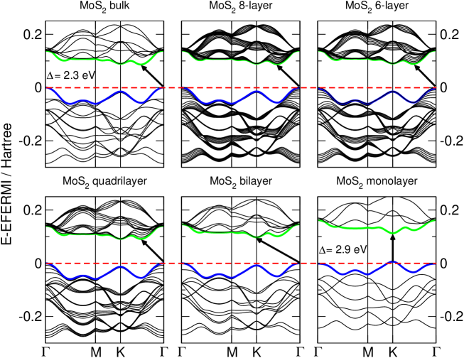
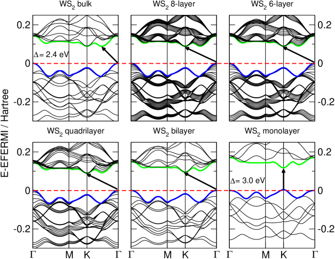
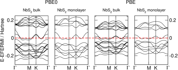
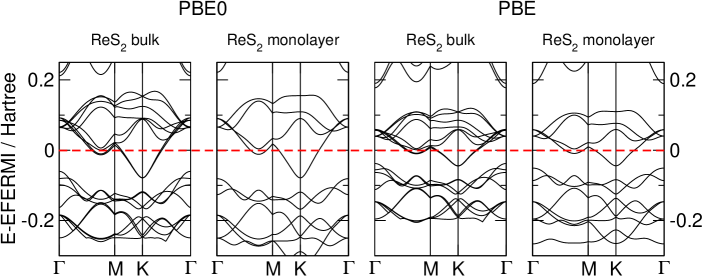
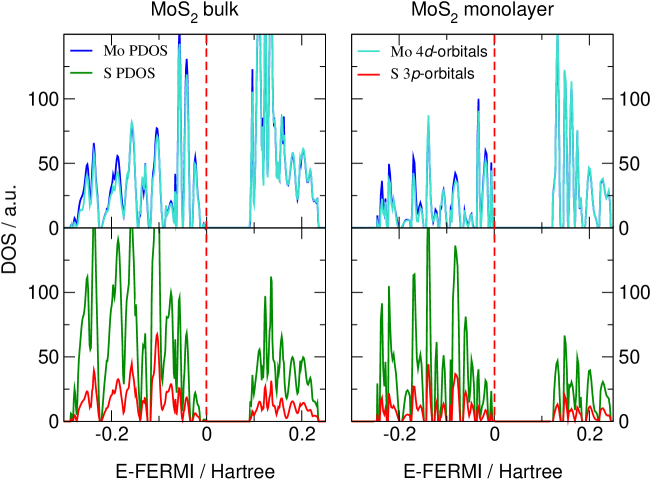
Figure 1: Band structures of bulk MoS2, its monolayer, as well as, polylayers calculated as the DFT/PBE0. The horizontal dashed lines indicate the Fermi level. The arrowas indicate the smallest value of the band gap (direct or indirect) for a given system.Figure 2: Band structures of bulk WS2, its monolayer, as well as, polylayers calculated as the DFT/PBE0. The horizontal dashed lines indicate the Fermi level. The arrowas indicate the smallest value of the band gap (direct or indirect) for a given system.Figure 3: Band structures of bulk NbS2 and its monolayer calculated as the DFT/PBE0 and the DFT/PBE. The horizontal dashed lines indicate the Fermi level. The arrowas indicate the smallest value of the band gap (direct or indirect) for a given system.Figure 4: Band structures of bulk ReS2 and its monolayer calculated as the DFT/PBE0 and the DFT/PBE. The horizontal dashed lines indicate the Fermi level. The arrowas indicate the smallest value of the band gap (direct or indirect) for a given system.Figure 5: Partial density of states of bulk MoS2 and its monolayer calculated as the DFT/PBE0. The projections of Mo and S atoms are given together with the contributions from 4 and 3 orbitals of Mo and S, respectively. The vertical dashed lines indicate the Fermi level. (Online color).