Characterizing top gated bilayer graphene interaction with its environment by Raman spectroscopy
Abstract
In this work we study the behavior of the optical phonon modes in bilayer graphene devices by applying top gate voltage, using Raman scattering. We observe the splitting of the Raman G band as we tune the Fermi level of the sample, which is explained in terms of mixing of the Raman () and infrared () phonon modes, due to different doping in the two layers. We theoretically analyze our data in terms of the bilayer graphene phonon self-energy which includes non-homogeneous charge carrier doping between the graphene layers. We show that the comparison between the experiment and theoretical model not only gives information about the total charge concentration in the bilayer graphene device, but also allows to separately quantify the amount of unintentional charge coming from the top and the bottom of the system, and therefore to characterize the interaction of bilayer graphene with its surrounding environment.
pacs:
02.20.-a, 78.30.-j, 78.67.-nBilayer graphene has attracted a lot of attention recently because of its special low energy electronic dispersion, in which a tunable band gap can be opened by application of a transverse electric field mccann ; netoreview ; ohta ; neto07biased ; oostinga07 ; wang2009 ; mak2009 ; kuzmenko-bandgap . Such device is desirable for low energy photo-emitters and detectors possessing a high tunability by the control of charge concentrations on the graphene layers. Recent experimental demonstration of this tunable band gap in bilayer graphene was based on the absorption measurements in the infrared region wang2009 ; mak2009 ; kuzmenko-bandgap or by electric transport measurementsneto07biased ; oostinga07 . However the tunable band gap bilayer graphene device operation can be greatly influenced by the surrounding environment. Typically, unintentional doping charges coming from the top and the bottom of the system can accumulate on bilayer graphene, giving rise to an unintentional electric field which determines a non-homogeneous doping between the layers and the opening of a band gap in the band structure, without any applied electric field paola . In this work we use Raman spectroscopy to monitor the unintentional charge coming from the top and the bottom of the system, which gives information on the electrostatic environment of the sample and which helps to characterize the bilayer devices for further applications.
The band gap opening and tunability in bilayer graphene is based on the application of an electric field perpendicular to the layers, given by where and are the charge carriers coming from the top and the bottom of bilayer graphene, respectively. Raman spectroscopy has already shown to be a fast and non-destructive tool to characterize graphene samples ferrari ; malard09 and doping effects pisana07 ; yan07 ; das08 ; das09 ; bruna , however no carefully analysis has been done to demonstrate the effect of non-homogeneous doping in bilayer graphene devices. Recent theoretical calculations made by Gava et al. paola suggest that from the analysis of the Raman spectra of gated bilayer graphene it is possible to quantitatively identify the amount of non-intentional charges coming from the atmosphere and from the substrate and to characterize the electrostatic environment of few-layers graphene. In this work we study the dependence of the G band of bilayer graphene on the gate voltage. From the direct comparison between the experimental and the theoretically simulated Raman spectra, and from the analysis of the positions, full width at half maximum (FWHM) and relative intensities of the two Raman peaks as a function of the electron concentration, we were able to estimate the charge unintentionally accumulated on the device from the environment.
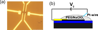
Fig. 1(a) shows the bilayer-graphene field-effect transistor (FET) used in the experiment. Graphene samples were produced by micro-mechanical cleavage of graphite and deposited on Si covered with 300nm of SiO2. Top gating was achieved by using a polymer electrolyte consisting of polyethylene glycol (PEG) and NaClO4 with ratio concentration of 1:0.25, and the gate voltage was applied between a gold electrode in contact with the graphene layer and a platinum wire electrode inserted in the electrolyte (see the schematic setup in Fig. 1(b)). The contacts were made by optical lithography. The Raman measurements were done in the back scattering configuration at room temperature using a triple monochromator spectrometer (DILOR XY) using 2.41 eV as excitation laser energy. The spot size of the laser was 1 m using a 80 objective and the laser power was kept at 1.4 mW.
The interface between graphene and polymer electrolyte has been shown experimentally to behave like a double layer capacitor of thickness in the order of nanometers bard . Therefore, the geometric capacitance of the electrolyte is very high compared to bottom gate devices where the thickness of the dielectric is much larger (typically 300 nm).
Capacitance measurements of the polymeric electrolyte used in the experiment were performed by Impedance Spectroscopy with frequency analyzer AUTOLAB PGSTAT30 by using a symmetrical cell with two Au electrodes and a polymer electrolyte layer. The impedance measurements for the electrolytes were carried out with frequency ranging from 50 kHz to 0.5 Hz at 0 V with 10 mV amplitude, and we obtained the value of 1.5 10-6 F cm-2. However, the shape and the thickness of the electrical double layer depends on the specific surface at contact with the electrolyte. Therefore, the measured value of CG only gives the order of magnitude of the geometric capacitance of the electrolyte in contact with bilayer graphene.
In the case of bilayer graphene with Bernal AB layer stacking, both the electronic and phonon bands split into two components with special symmetries tggraphene . The E2g phonon mode of monolayer graphene splits into two components, associated with the symmetric (S) and anti-symmetric (AS) displacements of the atoms in the two layers with respect to inversion symmetry malardprl08 . The S and AS modes belong to the two double degenerated representation Eg and Eu, respectively paola ; ando09 ; malardprl08 ; yan09 . The Eu mode is not Raman active and, therefore, the G band of isolated bilayer graphene is composed of only one peak. However, when the two layers of bilayer graphene have different charge carrier concentration, induced by the application of an external gate voltage, the inversion symmetry of bilayer graphene is broken, lowering the symmetry of the system. As a consequence of the induced asymmetry between the two layers, the two S and AS modes are mixed, the two new eigen-modes have the Raman active S component, and therefore two peaks are observed in the G band of bilayer graphene ando09 ; paola ; malardprl08 ; yan09 .
In Fig. 2(a) (red dashed curves) we show the experimental Raman spectra taken with the application of top gate voltage (Vg) from -1.50 to 1.00 V. The G band splitting into two components Gh and Gl (higher and lower frequency peak, respectively) can be clearly observed for Vg below -0.6 V. In order to compare the experimental spectra and theoretical calculations, we converted Vg into using the expression where the total capacitance , which includes the quantum capacitance (CQ) and geometrical capacitance (CG) das08 , and the intrinsic doping at the zero gate n0 are used as fitting parameters. Moreover, by the comparison between experimental and theoretical results we can estimate the charges unintentionally adsorbed, at zero gate, from the top and bottom of the device, and respectively. These quantities are related to n0 by , and therefore we only used n as additional fitting parameter. Finally, the theoretical FWHM calculated as a function of n and n is given by electron-phonon and an-harmonic phonon-phonon interaction paola . Therefore, in order to take into account other factors determining a finite lifetime and neglected in the calculations, we used in the fitting procedure a parameter , independent on the total charge and equal for the two peaks, related to the total FWHM by = + .
In Fig.2(a) we show the comparison between the experimental spectra (red dashed curve) and theoretical one (black continuous curve), obtained using the parameters discussed below, for different Vg. The fit is performed computing the square of the difference between the experimental and theoretical spectra, averaged over all the measured Raman range and over different Vg. We considered Vg in the range of 0.5 V. This choice is motivated by the fact that for large values of Vg the linear relation between gate voltage and charge could be modified, and charges from the electrolyte could accumulate on the bottom of the sample, making the fit results less reliable. The theoretical spectra is obtained as the sum of two Lorentzians, for the Gh and Gl frequency peaks. The two Lorentzians are centered in , with FWHMs = + , and with area Ih/l, where , , and Ih/l are computed as a function of and n. In particular, we used two different parameters, and , for positive and negative , which induce positive and negative (i.e. electron and hole doping charge), respectively. The values for the parameters used in the fit (i.e. , , n0, n, and ) are varied in uniform and dense grids. The best fit is obtained for = 3.7 and F cm-2, n cm-2, n = 0.0, and = 7.5 cm-1. Notice that the agreement between the experimental and simulated spectra is excellent in the range -0.5 to 0.5 V. The slight shifts out of this range can be ascribed to a possible hysteresis in the experiment, and to the fact that we did not consider in our model the expected jump of the quantum capacitance () when, increasing (decreasing) the Fermi level, we reach the second conduction band (penultimate valence band) in bilayer graphene das08 . The different values of and can be ascribed to the different mobilities of the positive () and negative () ions.
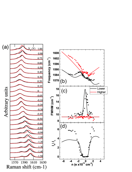
All the G band experimental spectra of Fig. 2(a) were fitted using two Lorentzians in order to extract the frequencies and full width at half maximum (FWHM) of two components Gh and Gl, as well as the relative Raman intensity, i.e., the ratio between the Raman intensities of the modes with highest frequency (Ih) and lowest frequency (Il). Figs. 2(b) and (c) shows, respectively, the dependence of the Gh (red dots) and Gl (black dots) frequencies and FWHM as a function of the electron concentration. The full lines are the theoretical calculations. The dependence of the frequency of the Gh and Gl Raman peaks (Fig. 2(b)) is well described by the calculation of the phonon self energy as a function of charge concentration. The distinct behaviors of the Gh and Gl is qualitatively explained by the distinct electron-phonon couplings of these modes. While Gh blue-shifts with charge carrier concentration due to inter-band transitions, the Gl mode redshifts due to intra-band transitions when the EF is changed. For the FWHM dependence, while does not change with , the is maximum near and minimum for values of corresponding to values of larger than half of the phonon energy, as has been observed before in both mono and bilayer graphene pisana07 ; yan07 ; das08 . It’s worth to mention that the scattered data points for the FHWM are mostly caused by charge carrier fluctuation during the measurement, where a hysteresis of the charge neutrality point is found by sweeping the gate voltage up and down. In Fig. 2(d) we plot the dependence of the Ih/Il as a function of . The quantity Ih/Il shows a minimum value between n -1 to 1 1013 cm-2, and increases more strongly for positive carrier concentration.
In summary, a detailed analysis of the G band of top gated bilayer graphene is presented. We observed that, unlike in the unbiased case where the G Raman band is composed by only one peak, the gate voltage breaks the inversion symmetry and the G band splits in two modes, that are combinations of the symmetric and anti-symmetric modes of the unbiased bilayer graphene. We analyze the dependence of the frequency and the relative intensities of the peaks with higher and lower frequency as a function of the electron concentration and we compared the experimental results with theoretical calculations. From this comparison, we could estimate the unintentional carrier concentration adsorbed on the device, at zero gate, from the substrate, , and from the electrolyte, , and we found and cm-2, showing that Raman spectroscopy is a powerful technique to study the electrostatic environment of graphene.
We would like to acknowledge Nacional de Grafite (Brazil) for providing us the graphite samples. D.L.M. and L.M.M. acknowledges the support from the Brazilian Agency CNPq.
References
- (1) E. McCann, Phys. Rev. B 74, 161403 (2006).
- (2) A. H. Castro Neto, F. Guinea, N. M. R. Peres, K. S. Novoselov, and A. K. Geim, Rev. Mod. Phys. 81, 109 (2009).
- (3) T. Ohta, A. Bostwick, T. Seyller, K. Horn and E. Rotenberg, Science 311, 951 (2006).
- (4) E. V. Castro, K. S. Novoselov, S. V. Morozov, N. M. Peres, J. M. dos Santos, J. Nilsson, F. Guinea, A. K. Geim, and A. H. Neto, Phys. Rev. Lett. 99, 216802 (2007).
- (5) Jeroen B. Oostinga, Hubert B. Heersche, Xinglan Liu, Alberto F. Morpurgo, and Lieven M. K. Vandersypen, Nature Materials 7, 151 (2007).
- (6) Y. Zhang, T. Tang, C. Girit, Z. Hao, M. C. Martin, A. Zettl, M. F. Crommie, Y. R. Shen and F. Wang, Nature 459, 820 (11 June 2009).
- (7) K. F. Mak, C. H. Lui, J. Shan and T. F. Heinz, Phys. Rev. Lett. 102, 256405 (2009).
- (8) A. B. Kuzmenko, E. van Heumen, D. van der Marel, P. Lerch, P. Blake, K. S. Novoselov, and A. K. Geim, Phys. Rev. B 79, 115441 (2009).
- (9) P. Gava, M. Lazzeri, A. M. Saitta, and F. Mauri, Phys. Rev. B 80, 155422 (2009).
- (10) A. C. Ferrari, J. C. Meyer, V. Scardaci, C. Casiraghi, M. Lazzeri, F. Mauri, S. Piscanec, D. Jiang, K. S. Novoselov, S. Roth, and A. K. Geim, Phys. Rev. Lett. 97, 187401 (2006).
- (11) L. M. Malard, M. A. Pimenta, G. Dresselhaus, and M. S. Dresselhaus, Phys. Rep. 473, 51 (2009).
- (12) S. Pisana, M. Lazzeri, C. Casiraghi, K. S. Novoselov, A. K. Geim, A. C. Ferrari and F. Mauri, Nature Mater. 6, 198 (2007).
- (13) J. Yan, Y. Zhang, P. Kim and A. Pinczuk, Phys. Rev. Lett. 98, 166802 (2007).
- (14) A. Das, S. Pisana, B. Chakraborty, S. Piscanec, S. K. Saha, U. V. Waghmare, K. S. Novoselov, H. R. Krishnamurthy, A. K. Geim, A. C. Ferrari and A. K. Sood, Nature Nanotech. 3, 210 (2008).
- (15) M. Bruna and S. Borini, Phys. Rev. B 81, 125421 (2010).
- (16) A. Das, B. Chakraborty, S. Piscanec, S. Pisana, A. K. Sood, and A. C. Ferrari, Phys. Rev. B 79, 155417 (2009).
- (17) L. M. Malard, M. H. D. Guimar es, D. L. Mafra, M. S. C. Mazzoni, and A. Jorio, Phys. Rev. B 79, 125426 (2009).
- (18) L. M. Malard, D. C. Elias, E. S. Alves, and M. A. Pimenta, Phys. Rev. Lett. 101, 257401 (2008).
- (19) T. Ando and M. Koshino, J. Phys. Soc. Jpn. 78, 034709 (2009).
- (20) J. Yan, T. Villarson, E. A. Henriksen, P. Kim, and A. Pinczuk, Phys. Rev. B 80, 241417(R) (2009).
- (21) A. J. Bard and L. R. Faulkner, ”Electrochemical Methods, Fundamentals and Applications”, John Wiley and Sons, New York, USA, 1980.