Spontaneously gapped ground state in suspended bilayer graphene
Abstract
Bilayer graphene bears an eight-fold degeneracy due to spin, valley and layer symmetry, allowing for a wealth of broken symmetry states induced by magnetic or electric fields, by strain, or even spontaneously by interaction. We study the electrical transport in clean current annealed suspended bilayer graphene. We find two kind of devices. In bilayers of type B1 the eight-fold zero-energy Landau level (LL) is partially lifted above a threshold field revealing an insulating quantum Hall state at the charge neutrality point (CNP). In bilayers of type B2 the LL lifting is full and a gap appears in the differential conductance even at zero magnetic field, suggesting an insulating spontaneously broken symmetry state. Unlike B1, the minimum conductance in B2 is not exponentially suppressed, but remains finite with a value even in a large magnetic field. We suggest that this phase of B2 is insulating in the bulk and bound by compressible edge states.
pacs:
72.80.Vp, 73.43.Qt, 73.23.-b, 73.22.Pr, 73.22.GkTwo dimensional electron systems (2DES) can host a large variety of ground states. Celebrated examples are the fractional quantum-Hall effect Tsui1982 ; Du2009 ; Bolotin2009 and the Wigner crystal Wigner1934 , both being driven by Coulomb interaction. Bilayer graphene provides a further class of interacting 2DES DasSarma2010 . In contrast to single layer graphene, the chiral charge carriers are massive due to the coupling between the two layers McCann2006a ; Novoselov2006 . Owing to the large number of symmetries, a wealth of ground states has been predicted Min2008 ; Nandkishore2010 ; Zhang2010 ; Nandkishore2010b ; Gorbar2010 ; Zhang2011 .
Bilayer graphene proves to be interesting in terms of electron-electron interaction. In comparison with single layer graphene the interaction parameter is about times higher and proportional to , where is the charge carrier density DasSarma2010 . The Coulomb interaction can even further be increased by suspending the sample. Furthermore, cleaner devices can be obtained by current annealing Moser2007 ; Bolotin2008 . The subsequently lower disorder potential enables one to reach a lower minimal carrier concentration at the charge neutrality point (CNP). At and around the CNP, electron-electron interaction has been predicted to be able to spontaneously open a gap Min2008 ; Nandkishore2010 ; Zhang2010 ; Nandkishore2010b ; Gorbar2010 ; Zhang2011 . This is opposed to an induced gap from the application of an external field McCann2006b ; Oostinga2008 ; Weitz2010 or mechanical strain Choi2010 ; Falko2011 .
Bilayer graphene has an eightfold degenerate LL at zero energy. As the Hall conductivity is quantized at values of , where the filling factor is given by , a step of 8 is observed from to around the CNP Novoselov2006 . The eightfold zero-energy LL degeneracy can be lifted. For example, the Zeeman energy is able to break the spin symmetry. This manifests itself in a partial lifting with a quantum Hall plateau appearing at Feldman2009 . A breaking of symmetries can also be induced by strong electron-electron interaction Nomura2006 ; Gorbar2010 . If all symmetries are lifted, quantum Hall plateaus appear at filling factors , , , , . Magnetic fields of T were required to see this lifting in silicon dioxide supported devices, for both single Zhang2006 and bilayer graphene Zhao2010 , until Feldman et al. succeeded in observing the effect at low magnetic fields in suspended bilayer graphene Feldman2009 .
The most striking state is the state, whose nature is under debate for both single layer Abanin2007 ; Checkelsky2009 ; Zhang2010a and bilayer graphene Feldman2009 ; Weitz2010 ; Zhao2010 . For bilayer graphene, several possibilities are being discussed, such as the quantum Hall ferromagnet (QHF) Nomura2006 ; Gorbar2010 , the quantum anomalous Hall insulator (AHI) Raghu2008 ; Nandkishore2010b , or a ferroelectric phase Zhang2010 . Using differential conductance spectroscopy, we find a new class of bilayer samples, which are evidentially gapped at the CNP in zero magnetic and electric field.
Suspended graphene devices were fabricated by mechanical exfoliation of natural graphite transferred to a doped Si wafer with a nm top SiO2 layer. The number of graphene layers was determined by Raman spectroscopy. The devices were then annealed for several hours in vacuum ( mbar) at ∘C before the electrical contacts made from Cr/Au (/ nm) bilayers were fabricated by electron-beam lithography. Thereafter, SiO2 was etched in buffered hydrofluoric acid (HF). After mounting a device into a 3He cryostat, we performed current annealing by applying a DC current at K. This procedure was repeated with higher currents until the electrical conductance as a function of the gate voltage applied to the doped substrate showed a pronounced dependence with a charge neutrality point (CNP), where has a minimum, close to , reminiscent of a high quality device (this usually required current densities of up to A/cm2). Conductance measurements were carried out with a lock-in amplifier applying a V AC voltage onto which a DC bias voltage could be superimposed.
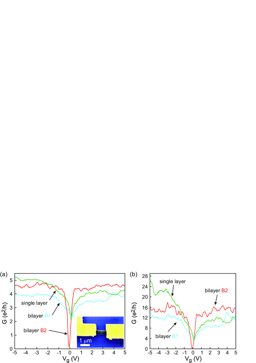
Fig. 1 shows representative measurements of the two-terminal conductance of suspended graphene devices when is altered by the back-gate voltage . The CNP is close to 0 V for all samples, indicating that only few charged impurities reside on the graphene. Both single layer and bilayers of type B1 display a smooth transition from low at the CNP to higher values at larger , as expected from the V-shaped conductances found in recent literature Morozov2008 ; Du2008 ; Feldman2009 . In contrast, bilayer samples of type B2 are very low conducting at the CNP with 0.2 at mK, which is considerably lower than in previous reports Weitz2010 . Furthermore, as the gate voltage is tuned away from the CNP, increases sharply and then quickly saturates for V. Note, that this is even the case, when the contact resistance is subtracted as shown in Fig. 1b.
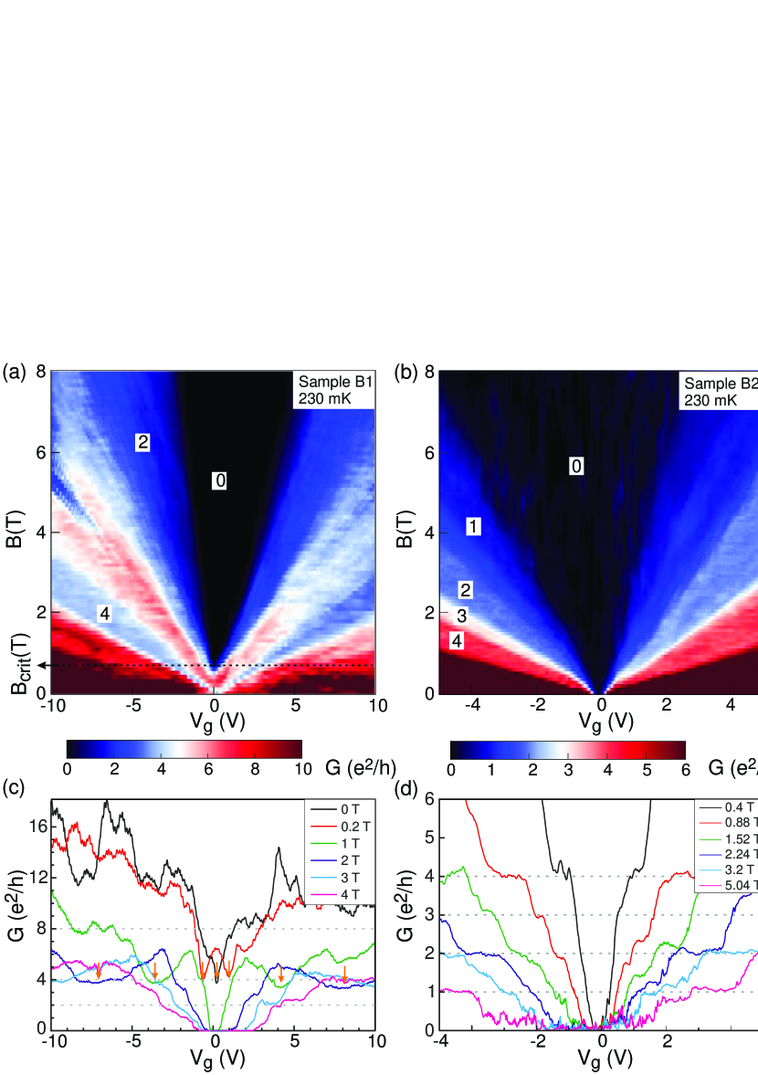
When placed in a perpendicular magnetic field , samples B1 and B2 reveal substantially different quantum Hall features, as shown in Fig. 2. As the measurements were performed in a two-terminal configuration, they include a contact resistance Williams2009 . We determine the contact resistance by matching to the closest integer value of the quantized Hall conductance (supplemental material supplemental ) and then subtracted it from the data. First, we discuss sample B1 and then sample B2.
In sample B1 we observe a partial lifting of the eightfold zero energy LL degeneracy, leading to the and states above a critical magnetic field of T (Fig. 2a). In the magnetic field range T we observe the same Hall sequence as in conventional devices where the conductance has a step of from to . When applying an insulating state emerges around the CNP, followed by the state with a two-fold degeneracy remaining. We also note that the state appears to extend all the way down to the CNP at zero magnetic field Martin2010 ; Nandkishore2010b . The corresponding line cuts from the color scale are shown in Fig. 2c to illustrate the evolution of the CNP into the state at low fields and the appearance of the broken symmetry states and at higher fields Feldman2009 . Unlike sample B1, B2 shows a fully lifted zero-energy LL, manifesting in the appearance of Hall plateaus for odd filling factors . In analogy to sample B1, we label the low conducting region around the CNP in sample B2 with , although this state maintains a finite conductance as we will discuss below.
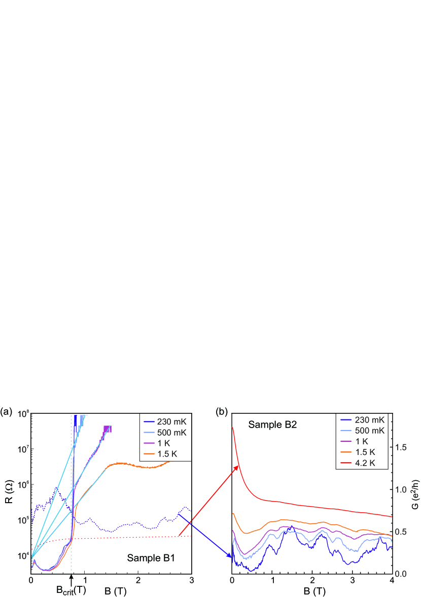
In the following Fig. 3 we investigate the properties of the low conducting state at at low charge carrier density as a function of and for both samples. For device B1 (Fig. 3a), we find that at low the resistance at the CNP remains around k, but when a critical perpendicular magnetic field of T is reached, it increases sharply to , the maximum resistance that our measurement set-up can resolve. This behavior can be attributed to the formation of a quantum Hall state at Checkelsky2009 . Since the Fermi energy now lies in between two Landau levels, a thermally activated behavior is expected for the electrical resistance . This is confirmed in the experiment, revealing a strong dependence of on temperature above the critical field following the law supplemental . The activation energy is linearly dependent on with a value that amounts to meV/T K/T. Note, that the spin Zeeman splitting is much smaller, only amounting to K/T. Feldman et al. Feldman2009 deduce in their experiment K/T, which is somewhat lower than our number. In a recent theory, taking interactions into account, the energy gap of the state has been calculated to be K/T Gorbar2010 .
The dotted curves in Fig. 3a show the resistance of B2 in direct comparison to that of B1 at mK and K. We find that at T B2 has an order of magnitude higher resistance than B1, whereas at higher magnetic fields, B1 is several orders more resistive. Fig. 3b elaborates on the conductance of B2 at the CNP as a function of and temperature. Most notably, at T is nearly independent of with the exception of fluctuations most likely due to localized states Bolotin2009 .
The marked differences in the magnetic field dependence clearly demonstrate that sample B1 and B2 differ. In sample B1, the LL degeneracy is partially lifted for T. This lifting includes a transition into a quantum Hall plateau in the vicinity of the CNP. On the other hand, sample B2 reveals a fully lifted LL, where all Hall plateaus appear already a small T. Furthermore, sample B2 stays conductive at the CNP even at higher of up to T. We note, that sample B1 is similar in characteristics to the one reported by Feldman et al. Feldman2009 , whereas B2 shows new features.
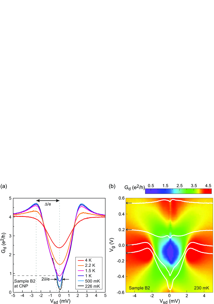
We further investigate the nature of sample B2 by measuring the differential conductance as a function of the applied DC bias between source and drain contacts at T at the CNP ( V), where is suppressed. Fig. 4a summarizes the findings for different temperatures from mK to K (no contact resistance subtracted). Two gaps can clearly be identified: When going from large source-drain bias mV towards small voltages, the larger gap sets in at mV, where is decreased from around to in the data measured at mK. The smaller gap appears at voltages mV and it reduces from to less than . By increasing the temperature from mK on, the smaller gap is first reduced and then vanishes at K.
In order to identify the origin of these two gaps, a color scale plot of the differential conductance against and the gate voltage at mK is shown in Fig. 4b. The line cut at the CNP ( V) shows again the two gaps in electron transport. As and thus the charge carrier concentration is increased, the two gaps exhibit distinct changes. The larger gap disappears, while the smaller gap still exists in the metallic graphene regime at V but the relative dip is less pronounced. This behavior is qualitatively consistent with Coulomb charging of the whole flake Devoret1990 . We estimate a single-electron charging energy of meV for a flake of width m. Because the contact conductances of are substantially larger than , charge quantization is only weak and no strong Coulomb blockade gap is expected. One rather expects the conductance to display a ‘weak’ conductance suppression by something like around zero bias, in agreement with the observation. In contrast to the small gap, the larger gap is strongly dependent on the charge carrier density. At the CNP, it has its maximum magnitude, but only slightly away it starts to close. The line cut at V already bears little sign of the gap . We therefore conclude that it must be a feature intrinsic to the low-energy band structure of bilayer graphene and that this gap is formed spontaneously at zero magnetic and at zero electric field. We emphasize that the electric field induced by the back-gate voltage in the vicinity of the gap feature of mV is negligible. In the tight-binding band structure calculation of McCann McCann2006b an induce a gap of mV, as we observe it in our experiment, would require a back-gate voltage of at least V. The gap can be associated with the state, as the low-conductance region in the color scale plot of Fig. 2b extends from large magnetic fields all the way down to zero magnetic field with no apparent phase boundary supplemental , distinctly different to the finding of Weitz et al. Weitz2010 . Although sample B1 and B2 have a state around the CNP in our argument, these states are electrically different. In sample B1, the resistance evidently increases to infinity, whereas it stays finite in B2. This difference can be explained by insulating phases, differing in their edge-state structure Raghu2008 ; Nandkishore2010b ; Zhang2011 .
Sample B1 has two phases, a low-magnetic field phase and a broken symmetry state induced by a small magnetic field of . The latter most likely is a quantum Hall ferromagnet Nomura2006 ; Gorbar2010 ; Nandkishore2010b . The phase at low magnetic field has been assigned to a gapped anomalous Hall insulator (AHI) in which topologically protected edge states should provide a conductance of up to Martin2010 ; Nandkishore2010b ; Zhang2011 . This scenario is somewhat supported by the quantum Hall states at that persist all the way down to (see arrows in Fig. 2c). A similar observation has been made in compressibility measurements by Martin et al. Martin2010 . Because B2 is the cleaner sample of the two comment , we rather think that low-field phase of B1 is a normal state, not a broken symmetry state. In contrast, the low-density phase of B2 is a broken symmetry state with edge states. If we subtract the small gap in sample B2, the measured conductance is , which is smaller than the ballistic channel conductance of any gapped phase with edge states. This suggests that the gapped phase is either not single domain or that the edge states are not topologically protected, allowing for partial back-scattering. Further work is needed to determine the nature of the edge states and assign it to broken electron-hole, valley or spin-symmetry Abanin2006 ; Martin2008 ; Nandkishore2010b ; Zhang2011 .
In conclusion, using differential conductance spectroscopy we found a new type of bilayer whose spectral density is gapped at zero magnetic and zero electric field. Though this state is due to an insulating phase, the non-vanishing conductance , which is surprisingly robust in magnetic field, suggests that edge states are present.
This work was financed by the Swiss NSF, the ESF programme Eurographene, the NCCR Nano and the NCCR Quantum. We acknowledge access to Raman microscope provided by C. Stampfer and C. Hierold. We are also grateful to A. Baumgartner, D. Maslov, A. Morpurgo, A. Yacoby, V. Fal’ko and L. Levitov for discussions.
References
- (1) D. C. Tsui, H. L. Stormer, and A. C. Gossard, Phys. Rev. Lett. 48, 1559 (1982).
- (2) X. Du, I. Skachko, F. Duerr, A. Luican, and E. Y. Andrei, Nature 462, 192 (2009).
- (3) K. I. Bolotin, F. Ghahari, M. D. Shulman, H. L. Stormer, and P. Kim, Nature 462, 196 (2009).
- (4) E. Wigner, Phys. Rev. 46, 1002 (1934).
- (5) S. Das Sarma, S. Adam, E. H. Hwang, and E. Rossi, Rev. Mod. Phys. 83, 407 (2011).
- (6) E. McCann and V. I. Fal’ko, Phys. Rev. Lett. 96, 086805 (2006).
- (7) K. S. Novoselov, E. McCann, S. V. Morozovi, V. I. Fal’ko, M. I. Katsnelson, U. Zettler, D. Jiang, F. Schnedin, and A. K. Geim, Nature Phys. 2, 177 (2006).
- (8) H. Min, G. Borghi, M. Polini, and A. H. MacDonald, Phys. Rev. B 77, 041407(R) (2008).
- (9) R. Nandkishore and L. Levitov, Phys. Rev. Lett. 104, 156803 (2010).
- (10) F. Zhang, H. Min, M. Polini, and A. H. MacDonald, Phys. Rev. B 81, 041402 (2010).
- (11) R. Nandkishore and L. Levitov, Phys. Rev. B 82, 115124 (2010).
- (12) E. V. Gorbar, V. P. Gusynin, and V. A. Miransky, JETP Letters, 91, 314 (2010).
- (13) F. Zhang, J. Jung, G. A. Fiete, Q. Niu, and A. H. MacDonald, Phys. Rev. Lett. 106, 156801 (2011).
- (14) J. Moser, A. Barreiro, and A. Bachtold, Appl. Phys. Lett. 91, 163513 (2007).
- (15) K. Bolotin, K. J. Sikes, Z. Jiang, M. Klima, G. Fudenberg, J. Hone, P. Kim, and H. L. Stormer, Solid State Commun. 146, 351 (2008).
- (16) E. McCann Phys. Rev. B 74, 161403(R) (2006).
- (17) J. B. Oostinga, H. B. Heersche, X. Liu, A. F. Morpurgo, and L. M. K. Vandersypen, Nature Mater. 7, 151 (2008).
- (18) R. T. Weitz, M. T. Allen, B. E. Feldman, J. Martin, and A. Yacoby, Science 330, 812 (2010).
- (19) S.-M. Choi, S.-H. Jhi, and Y.-W. Son, Nano Lett. 10, 3486 (2010).
- (20) M. Mucha-Kruczynski, I. Aleiner and V. Fal’ko, arXiv:1104.5029.
- (21) B. E. Feldman, J. Martin, and A. Yacoby, Nature Phys. 5, 889 (2009).
- (22) K. Nomura and A. H. MacDonald, Phys. Rev. Lett. 96, 256602 (2006).
- (23) Y. Zhang, Z. Jiang, J. P. Small, M. S. Purewal, Y.-W. Tan, M. Fazlollahi, J. D. Chudow, J. A. Jaszczak, H. L. Stormer, and P. Kim Phys. Rev. Lett. 96, 136806 (2006).
- (24) Y. Zhao, P. Cadden-Zimansky, Z. Jiang, and P. Kim, Phys. Rev. Lett. 104, 066801 (2010).
- (25) D. A. Abanin, K. S. Novoselov, U. Zeitler, P. A. Lee, A. K. Geim, and L. S. Levitov, Phys. Rev. Lett. 98, 196806 (2007).
- (26) J. G. Checkelsky, L. Li, and N. P. Ong, Phys. Rev. B 79, 115434 (2009).
- (27) L. Zhang, Y. Zhang, M. Khodas, T. Valla, and I. A. Zaliznyak, Phys. Rev. Lett. 105 046804 (2010).
- (28) S. Raghu, X.-L. Qi, C. Honerkamp, and S.-C. Zhang, Phys. Rev. Lett. 100, 156401 (2008).
- (29) S. V. Morozov, K. S. Novoselov, M. I. Katsnelson, F. Schedin, D. C. Elias, J. A. Jaszczak, and A. K. Geim, Phys. Rev. Lett. 100, 016602 (2008).
- (30) X. Du, I. Skachko, A. Barker, and E. Y. Andrei, Nature Nanotech. 3, 491 (2008).
- (31) J. R. Williams, D. A. Abanin, L. DiCarlo, L. S. Levitov, and C. M. Marcus, Phys. Rev. B 80, 045408 (2009).
- (32) See supplementary material at http://link.aps.org/supplemental/…
- (33) J. Martin, B. E. Feldman, R. T. Weitz, M. T. Allen, and A. Yacoby, Phys. Rev. Lett. 105, 256806 (2010).
- (34) M. H. Devoret, D. Esteve, H. Grabert, G. L. Ingold, H. Pothier, and C. Urbina, Phys. Rev. Lett. 64, 1824 (1990).
- (35) We can convert B2 into B1 by exposing the sample to air. To convert B1 into B2 requires current annealing at low temperatures.
- (36) D. A. Abanin, P. A. Lee, and L. S. Levitov, Phys. Rev. Lett. 96, 176803 (2006).
- (37) I. Martin, Y. M. Blanter, and A. F. Morpurgo, Phys. Rev. Lett. 100, 036804 (2008).