Raman spectroscopy on etched graphene nanoribbons
Abstract
We investigate etched single-layer graphene nanoribbons with different widths ranging from 30 to 130 nm by confocal Raman spectroscopy. We show that the D-line intensity only depends on the edge-region of the nanoribbon and that consequently the fabrication process does not introduce bulk defects. In contrast, the G- and the 2D-lines scale linearly with the irradiated area and therefore with the width of the ribbons. We further give indications that the D- to G-line ratio can be used to gain information about the crystallographic orientation of the underlying graphene. Finally, we perform polarization angle dependent measurements to analyze the nanoribbon edge-regions.
pacs:
71.15.Mb, 81.05.ue, 63.22.Rc, 78.67.Wj, 78.30.NaIntroduction
Graphene nanoribbons han07 ; lin08 ; wan08 ; mol09b ; han09 ; mol10 ; gal10 attract increasing attention due to the possibility of building graphene-based nanoelectronics as for example field-effect transistors wan08 ; zha08 or quantum dot devices sta08a ; pon08 . In contrast to two-dimensional gapless bulk graphene gei07 , it has been shown that confinement fer07a ; yan07a , disorder sol07 and edge effects yan07a introduce a transport gap in graphene nanoribbons. The fabrication technique may influence the transport properties of the nanoribbons in terms of added bulk and/or edge disorder. Disorder is expected to strongly influence the scaling behavior of the energy gap as a function of the nanoribbon width and the local doping profile mol09b ; han09 ; mol10 ; gal10 . In addition, very little is known about the edge structure and theoretical investigations of the vibrational properties of nanoribbons have only been started very recently gil09 . Raman spectroscopy on carbon (nano)materials mal09 ; fer07 has been recognized as a powerful technique not only for probing selected phonons, but also for identifying the number of graphene layers fer06 ; dav07a , for determining local doping levels sta07aa , for studying electron-phonon coupling pis07 and thus for the electronic properties themselves.
In this letter we report Raman spectroscopy experiments on etched graphene nanoribbons with different widths ranging from 30 to 130 nm (schematic in Fig. 1a). We show that the characteristic signatures of single-layer graphene (SLG) in the Raman spectra are still well preserved, that the absolute G- and 2D-line intensities scale with the nanoribbon width, whereas the D-line intensity does not. Consequently, the D-line intensity depends only on the edge-region of the nanoribbon including the edge roughness which can be further analyzed by performing polarization dependent measurements.
Fabrication
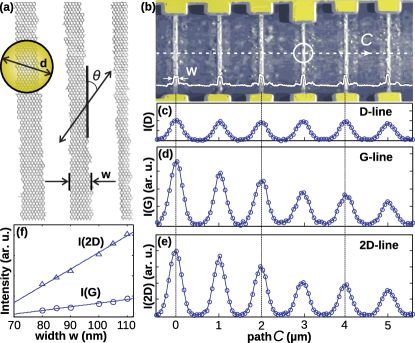
The nanoribbon fabrication is based on the mechanical exfoliation of natural graphite nov04 , electron beam lithography, reactive ion etching and metal evaporation. For details see Ref. mol09b . The graphene flakes have been identified to consist of a single-layer by measuring the Raman full width at half maximum (FWHM) of the 2D-line prior to processing fer06 ; dav07a . In Fig. 1b we show a scanning force microscope (SFM) image of six etched graphene nanoribbons with different widths. In total, we have studied three such nanoribbon arrays fabricated from three different single-layer flakes resulting in a total of more than 20 individual nanoribbons.
Experimental Setup
All Raman spectra were acquired using a green laser (532 nm, 2.33 eV). Employing a long working distance focusing lens (numerical aperture = 0.80), we obtain a spot size with a diameter 400 nm. The incident light was – unless stated differently – linearly polarized parallel to the macroscopic edge of the nanoribbons () and detection was always insensitive to polarization. The laser power was set to 2 mW in order to exclude heating effects and all measurements were conducted at room temperature.
Results
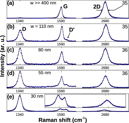
A selection of Raman spectra of nanoribbons with different widths is shown in Fig. 2. In all measurements, the characteristic signatures of graphene Raman spectra can be well identified: The defect induced D-line (1340 cm-1), the G-line (1580-1590 cm-1), the 2D-line (2680 cm-1) and for the thinner ribbons an additional defect induced D’-line (1620 cm-1). For a detailed review on the microscopic nature of all these lines, see Refs. tho00 ; rei04 ; fer06 ; dav07a ; fer07 ; pis07 ; mal09 .
The FWHM of the 2D-line with values below 40 cm-1 (see right labels in Figs. 2a-d) is a strong signature for the single-layer nature of the graphene nanoribbons fer06 ; dav07a . In order to enhance the signal for thin nanoribbons, we recorded the spectra of the 30 nm nanoribbon on a sub-array of several closely spaced nanoribbons with equal width (approx. 6 ribbons irradiated by the laser). This sample averaging may also explain the rather large but still single-layer FWHM of the 2D-line of nearly 50 cm-1. In contrast to defectless bulk graphene where significant D- and D’-lines are rarely present, we observe strong D- and D’-lines in the recorded spectra as the edges act as defects and allow elastic inter-valley scattering of electrons can04 ; can04a ; cas09 .
As demonstrated in Fig. 1c, the D-line intensity does not depend on the width of the nanoribbons. The peak width in Figs. 1c-e arises from strong spatial oversampling as the laser spot size ( 400 nm) is significantly larger than the step size ( 70 nm). As the laser spot size is also significantly larger than the nanoribbon width (), the total irradiated edge length is approximately (left and right edge) – independent of the nanoribbon width. As long as there is no bulk disorder present, the intensity of the D-line is not expected to depend on the nanoribbon width. This is observed in Fig. 1c and leads to the important conclusion that the reactive ion etching process used to pattern nanoribbons does not introduce a detectable amount of bulk defects into our graphene nanostructures.
In contrast to the D-line, we observe a width dependence of the G- and 2D-line intensities as shown in Figs. 1d,e. The intensity of the G-line is a function of the amount of irradiated sp2 bound carbon atoms mal09 and therefore expected to directly depend on the graphene nanoribbon area below the laser spot (). The same proportionality also holds for the 2D-line tui70 ; cas01 ; Laz08 . This expected linear dependence of the G- and 2D-line heights is confirmed in Fig. 1f (see lines fitted to circles and triangles). It is crucial to note that Fig. 1f does not allow to determine the width of a possibly existing Raman-inactive edge-region han07 . This is due to offsets in Figs. 1c-e (background of the Si substrate) and due to the inherent noise in the measurement, which masks the small line heights resulting from the short integration time. From the fact that we can measure 30 nm wide nanoribbons (see Fig. 2e), we conclude that such a Raman-inactive edge-region must either be significantly smaller than 15 nm or scale with the nanoribbon width.
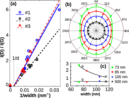
In order to compare the three arrays (), we show in Fig. 3a the intensity ratio versus the inverse ribbon width. Each array is made from a single SLG flake and all nanoribbons on a specific array were etched in the same processing step and are oriented parallel to each other. As a measure for the intensity, the peak area was used com0f . Based on the previous argument, the relation is expected and observed. It is important to note that this relation only holds in the limit (otherwise there is no edge located under the laser spot). Therefore, a linear fit was performed for each array and the intersection of the fit with the abscissa was pinned to .
Interestingly, the fits for the different arrays exhibit different slopes. There are two possible explanations: (i) The edge roughness differs for the different arrays: Rougher edges result in more defects illuminated by the laser spot and therefore a higher D-line intensity. As all the arrays were fabricated using the same process, this is improbable. (ii) The slopes can also be attributed to different crystallographic orientations of the graphene relative to the edge. This is because perfect zig-zag edges do not activate the D-line due to momentum conservation can04 ; can04a , whereas armchair segments do. While the plasma etched edges are certainly rough, the ratio of zig-zag to armchair segments should nevertheless depend on the overall crystallographic orientation relative to the nanoribbon orientation.
In Fig. 3b, we show the ratio for different nanoribbons of one array as a function of the incident photon polarization angle . For each ribbon and each angle, a spectrum was recorded and both the G- and the D-line were fitted each with a single Lorentzian. Geometric considerations suggesting mirror planes at 0∘ and 90∘ are confirmed. For Raman measurements in graphene, only phonon wave vectors perpendicular to the incident light polarization contribute to the signal gru03 ; can04a . As phonon wave vectors along the principal nanoribbon axis (i.e. 90∘ and 270∘) see little of the edges, the D-line is expected to be more suppressed than at all other angles.
Following Casiraghi et al. cas09 describing similar measurements on graphene edges and taking into account that does not depend on com0c , the following expression can be derived: , where and . This relation was used to fit the data and indeed a strong width dependence of and an overall constant of 0.55 only depending on the structure of the edges are found (Fig. 3.c). According to Ref. cas09 , a lower bound of the edge disorder correlation length can be estimated by 1 nm, which is in reasonable agreement with current fabrication limitations com0a .
Conclusion
In conclusion, we have demonstrated that the D- and D’-line depend only on the nanoribbon edge-region whereas the G- and the 2D-line scale with the illuminated area. We have shown that our fabrication process does not introduce bulk defects and that the ratio can give indications about the crystallographic orientation of graphene. These insights may help in designing further experiments and designing future graphene nanoelectronic devices.
Acknowledgment
The authors thank C. Casiraghi, A. C. Ferrari, M. Haluska, A. Jorio and L. Wirtz for helpful discussions and C. Hierold for providing access to the Raman spectrometer. Support by SNSF and NCCR nanoscience is gratefully acknowledged.
References
- (1) M. Y. Han, B. Özyilmaz, Y. Zhang, P. Kim, Phys. Rev. Lett. 98, 206805 (2007).
- (2) Y.-M. Lin, V. Perebeinos, Z. Chen, P. Avouris, Phys. Rev. B 78, 161409(R) (2008).
- (3) X. Wang, Y. Ouyang, X. Li, H. Wang, J. Guo, H. Dai, Phys. Rev. Lett. 100, 206803 (2008).
- (4) F. Molitor, C. Stampfer, J. Güttinger, A. Jacobsen, T. Ihn, K. Ensslin, Semicond. Sci. Technol. 24, 034002 (2009).
- (5) M. Y. Han, J. Brant, P. Kim, Phys. Rev. Lett. 104, 056801 (2009).
- (6) F. Molitor, A. Jacobsen, C. Stampfer, J. Güttinger, T. Ihn, K. Ensslin, Phys. Rev. B 79, 075426 (2010).
- (7) P. Gallagher, K. Todd, D. Goldhaber-Gordon, Phys. Rev. B 81, 115409 (2010).
- (8) Q. Zhang, T. Fang, H. Xing, A. Seabaugh, D. Jena, Electron Device Letters IEEE 12, 1344 (2008).
- (9) C. Stampfer, E. Schurtenberger, F. Molitor, J. Güttinger, T. Ihn, K. Ensslin, Nano Lett. 8, 2378 (2008).
- (10) L. A. Ponomarenko, F. Schedin, M. I. Katsnelson, R. Yang, E. H. Hill, K. S. Novoselov, A. K. Geim, Science 320, 356 (2008).
- (11) A. K. Geim, K. S. Novoselov, Nat. Mater. 6, 183 (2007).
- (12) J. Fernandez-Rossier, J. J. Palacios, L. Brey, Phys. Rev. B 75, 205441 (2007).
- (13) L. Yang, C.-H. Park, Y.-W. Son, M. L. Cohen, S. G. Louie, Phys. Rev. Lett. 99, 186801 (2007).
- (14) F. Sols, F. Guinea, A. H. Castro Neto, Phys. Rev. Lett. 99, 166803 (2007).
- (15) R. Gillen, M. Mohr, C. Thomsen, J. Maultzsch, Phys. Rev. B 80, 155418 (2009).
- (16) L. M. Malard, M. A. Pimenta, G. Dresselhaus, M. S. Dresselhaus, Phys. Rep. 473, 51 (2009).
- (17) A. C. Ferrari, Solid State Commun. 143, 47 (2007).
- (18) A. C. Ferrari, J. C. Meyer, V. Scardaci, C. Casiraghi, M. Lazzeri, F. Mauri, S. Piscanec, D. Jiang, K. S. Novoselov, S. Roth, A. K. Geim, Phys. Rev. Lett. 97, 187401 (2006).
- (19) D. Graf, F. Molitor, K. Ensslin, C. Stampfer, A. Jungen, C. Hierold, L. Wirtz, Nano Lett. 7, 238 (2007).
- (20) C. Stampfer, F. Molitor, D. Graf, K. Ensslin, A. Jungen, C. Hierold, L. Wirtz, Appl. Phys. Lett. 91, 241907 (2007).
- (21) S. Pisana, M. Lazzeri, C. Casiraghi, K. S. Novoselov, A. K. Geim, A. C. Ferrari, F. Mauri, Nature Mat. 6, 198, (2007).
- (22) K. S. Novoselov, A. K. Geim, S. V. Morozov, D. Jiang, M. I. Katsnelson, S. V. Dubonos, I. V. Grigorieva, A. A. Firsov, Science 306, 666, (2004).
- (23) S. Reich, C. Thomsen, Phil. Trans. R. Soc. Lond. A 362, 2271 (2004).
- (24) C. Thomsen, S. Reich, Phys. Rev. Lett. 85, 5214 (2000).
- (25) L. G. Cançado, M. A. Pimenta, B. R. A. Neves, M. S. S. Dantas, A. Jorio, Phys. Rev. Lett. 93, 247401 (2004).
- (26) L. G. Cançado, M. A. Pimenta, B. R. A. Neves, G. Medeiros-Ribeiro, T. Enoki, Y. Kobayashi, K. Takai, K. Fukui, M. S. Dresselhaus, R. Saito, A. Jorio, Phys. Rev. Lett. 93, 047403 (2004).
- (27) C. Casiraghi, A. Hartschuh, H. Qian, S. Piscanec, C. Georgi, K.S. Novoselov, D. M. Basko, A.C. Ferrari, Nano Lett. 9, 1433 (2009).
- (28) F. Tuinstra, J. L. Koening, J. Chem. Phys. 35, 1126, (1970).
- (29) C. Castiglioni, F. Negri, M. Rigolio, G. Zerbi, J. Chem. Phys. 115, 3769, (2001).
- (30) M. Lazzeri, C. Attaccalite, L. Wirtz, F. Mauri, Phys. Rev. B 78, 081406 (2008).
- (31) The area can be more accurately determined than the height and the area represents all photons/phonons participating in the Raman process.
- (32) A. Grüneis, R. Saito, Ge. G. Samsonidze, T. Kimura, M. A. Pimenta, A. Jorio, A. G. Souza Filho, G. Dresselhaus, M. S. Dresselhaus, Phys. Rev. B 67, 165402 (2003).
- (33) It is hard to prove that the G-line intensity is independent of , as even the slightest change in the focus of the Raman spectrometer changes the signal intensity. We therefore always use ratios when comparing line intensities.
- (34) Here we assume that the length of the local armchair segments is significantly larger than the carbon-carbon bond length. The disordered edge direction somewhere between averaged armchair or zigzag direction is not known and therefore only a very rough estimate on the lower bound can be made cas09 .