Quantum reflection of ultracold atoms from thin films, graphene, and semiconductor heterostructures
Abstract
We show that thin dielectric films can be used to enhance the performance of passive atomic mirrors by enabling quantum reflection probabilities of over 90% for atoms incident at velocities mm s-1, achieved in recent experiments. This enhancement is brought about by weakening the Casimir-Polder attraction between the atom and the surface, which induces the quantum reflection. We show that suspended graphene membranes also produce higher quantum reflection probabilities than bulk matter. Temporal changes in the electrical resistance of such membranes, produced as atoms stick to the surface, can be used to monitor the reflection process, non-invasively and in real time. The resistance change allows the reflection probability to be determined purely from electrical measurements without needing to image the reflected atom cloud optically. Finally, we show how perfect atom mirrors may be manufactured from semiconductor heterostructures, which employ an embedded two-dimensional electron gas to tailor the atom-surface interaction and so enhance the reflection by classical means.
pacs:
34.35.+a, 03.75.-b, 73.90.+f, 73.22.PrI Introduction
Hybrid quantum systems, which combine coherent cold atoms with solid structures, hold great promise for both fundamental science and technological applications. There are, for example, exciting possibilities for creating a new generation of devices to measure precisely, and image spatially, gravitational, electric and magnetic fields. Such devices have a key advantage over laser-based technology because atoms couple much more strongly than photons to gravitational and electromagnetic fields. Mirrors are integral to laser devices and the development of analogous matter-wave reflectors is of similar importance for developing atom optics. Despite considerable progress in manipulating atoms with solids, atom-mirror technology has not become either standardized or commercially available. Classical reflection of atoms has been achieved using light sheets, wire gratings and evanescent waves Bongs et al. (1999); Roach et al. (1995); Bender et al. (2010); Judd et al. (2008) but the technology is difficult to implement. Using a passive surface, and relying on quantum reflection, offers greater simplicity and flexibility in terms of potential landscape design. Quantum reflection of alkali atoms from the sharp Casimir-Polder (CP) potential step, found a few micrometres from a solid surface, has been demonstrated but, for Bose-Einstein condensates (BECs), the highest reflection probability seen so far is Pasquini et al. (2004, 2006). For single atoms, reflection probabilities approaching unity have been observed but only for very light atoms, which approach the surface at extremely acute angles of incidence Shimizu (2001).
Quantum reflection is a phenomenon whereby particles can reflect from a scattering potential in the absence of a classical turning point. It occurs at a sharp potential drop. The condition for strong quantum reflection is Shimizu (2001) where the local wave number, , depends on the de Broglie wavelength, , for the atom’s centre-of-mass motion, and is the normal distance from the atom to the surface. The mutual van der Waals attraction between an atom and a surface creates a sharp CP potential, which can satisfy the quantum reflection condition. In addition to prospective applications in passive atom-optical mirrors, quantum reflection can also yield information, which is hard to obtain by other means, about the CP potential profile for atoms near both planar and patterned surfaces Pasquini et al. (2004, 2006) and about atom-atom interactions within a BEC: for example soliton and vortex production during reflection Scott et al. (2005).
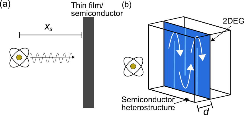
Here, we show that quantum reflection probabilities can be increased to over 90% for experimentally-accessible velocities Pasquini et al. (2004, 2006) by reducing the thickness of the surface structure. Figure 1(a) shows a schematic diagram of an alkali atom approaching a thin dielectric surface. We find that a nm-thick dielectric film gives the highest levels of quantum reflection. A suspended graphene membrane described using a Dirac electron model also produces quantum reflection probabilities significantly higher than for bulk surfaces, and comparable with the thinnest available dielectric sheets. However, if the graphene membrane is treated within a two-dimensional plasma sheet (hydrodynamic) model Churkin et al. (2010), the reflection probabilities are lower than for a bulk dielectric. At present there are uncertainties in the application and validity regimes of these models. Our analysis confirms predictions by Churkin et al. that present quantum reflection experiments are accurate enough to distinguish between them Churkin et al. (2010).
We show that free-standing graphene membranes offer two key advantages over bulk surfaces and dielectric membranes for quantum reflection studies. Firstly, the membrane can be cleaned between successive quantum reflection runs by passing a current through the membrane in order to heat it and so remove adsorbates. Such adsorbates are undesirable because they can strongly affect the atom-surface potential and so complicate the analysis of experimental data Pasquini et al. (2004, 2006). Secondly, the spatio-temporal dynamics of the reflecting cloud, and its reflection probability, can both be determined non-invasively and in real time by measuring changes in the membrane’s electrical resistance produced by the adsorption of those atoms that do not quantum reflect. In contrast to previous optical imaging, the electrical measurements that we propose can monitor the time evolution of the atom cloud throughout a single quantum reflection event and are unaffected by fragmentation of the atom cloud that occurs at low approach velocities Pasquini et al. (2004, 2006); Scott et al. (2005).
Finally, we explore the possibility of creating perfectly reflecting atom mirrors in which the reflection is enhanced by an array of wires only nm thick, buried in a semiconductor heterostructure. We find that 100% reflection can be achieved with just A wire currents: low enough for the wire array to be formed in a high-quality two-dimensional electron gas (2DEG) Judd et al. (2010); Sinuco-León et al. (2011) by using ion-beam implantation to create insulating channels, which define the wires. The architecture of this system is shown in figure 1(b) where the dark (light) blue areas represent the 2DEG (insulating channels) and the white arrows indicate the current flow.
The paper is structured as follows. In Section II, we investigate pure quantum reflection from thin dielectric glass films. In Section III, we consider quantum reflection from a suspended graphene membrane and quantify the effect that adsorbed atoms have on the membrane’s electrical resistance. In Section IV, we explore the effect of a 2DEG wire array on classical and quantum reflection from a gallium arsenide (GaAs) semiconductor surface. Finally, in Section V we draw conclusions and suggest promising directions for further theoretical work and experiments.
II Quantum Reflection from Dielectric Films
We begin by studying how the properties of thin dielectric films affect the quantum reflection probability, , of a 7Li atom approaching the film at normal incidence with velocity . The range 1-5 mm s-1 shown in figure 2 corresponds to that already attained experimentally for ultracold atoms Pasquini et al. (2004, 2006). Lithium-7 is particularly suitable for quantum reflection because it is comparatively light, which ensures maximal for a given , and Bose-condensable Bradley et al. (1997); Pollack et al. (2009). Further advantages are the low electrical polarizability compared with other alkali atoms, and the tuneability of inter-atomic interactions within a 7Li BEC from repulsive to attractive. These factors reduce topological cloud disruption that can occur when a BEC reflects Scott et al. (2005); Cornish et al. (2009); Pasquini et al. (2006), surface overlap, potential screening, and atom losses due to the quantum pressure of the wavepacket Scott et al. (2005); Cornish et al. (2009). If these issues can be circumvented, reflection probabilities for BECs are approximately the same as those for plane waves.
We first consider how the thickness, , of the dielectric film affects the CP potential, , and hence, . We calculate between an atom and the film using the Lifshitz approach Babb et al. (2004); Reyes and Eberlein (2009); Scheel and Buhmann (2008)
| (1) |
where is the speed of light in a vacuum, K is the temperature of both the surface and the environment, approximates the polarizability of 7Li at the imaginary Matsubara frequency with mode number , Fm2 is the static polarizability, rad s-1 is the transition frequency at a wavelength of nm (the dominant Lithium spectral line), and and are, respectively, the transverse magnetic and electric reflection probabilities of the surface. These photonic reflection coefficients are determined at each Matsubara frequency and wave number, , which relates to the variable of integration in (II) by . The dash (′) on the Matsubara sum implies half weight for the term. Other symbols have their usual meaning. For m, the values of obtained at K are very similar to those at . As quantum reflection zones (i.e. regions of in which ) can extend beyond m from the surface, we use the full finite-temperature theory to incorporate small corrections due to black-body radiation interacting with the atoms.
Lifshitz theory was found to be consistent, at the relevant distances, with the results of Bender et al. who measured the Casimir-Polder potential between an alkali atom and a glass surface Bender et al. (2010). Stray electric fields and adatoms were ignored and the good agreement between experiment and calculations of the bare Casimir-Polder potential support this. Limiting forms of Lifshitz theory were also used to calculate quantum reflection probabilities from a semiconductor surface Pasquini et al. (2004, 2006). For most velocities, good agreement was found with the experimental data. At low velocities (mm s-1), deviations were attributed to technical issues. When comparing Lifshitz theory with experiment it is sometimes necessary to consider corrections due to effects such as surface roughness Klimchitskaya et al. (2009). The experiments suggest that such effects can be neglected to a good approximation in our case.
The different types of thin film that we consider have different and . In the case of a dielectric slab of width , the reflection coefficients are given by Bordag et al. (2006)
| (2) |
where
| (3) |
is the electromagnetic wave number inside the slab. To evaluate and , we also require a dielectric response function . We take bulk SiO2 as this is a good insulator and films can be manufactured down to thicknesses of a few nanometres. The dielectric function of bulk SiO2 may be obtained to good approximation by using the following standard procedure: we use experimental values taken at real frequencies Palik (1985) and, for ease of computation, project these data onto the imaginary frequency axis using Kramers-Kronig relations Jackson (1975).
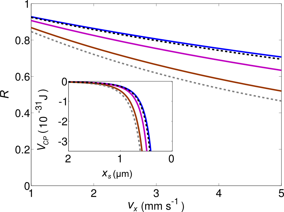
We begin by considering atomic quantum reflection from dielectric slabs with three thicknesses: m, nm and nm. We calculate using equations (II)-(3). We then use this potential to calculate for incident 7Li plane waves using the transfer matrix method Gilmore (2004).
In figure 2, the solid brown curve (2nd from bottom) shows calculated for a m film, which is, in effect, a bulk system since is much greater than the separation (typically m) of the quantum reflection zone (where ) from the surface. The solid magenta curve (3rd from top) is calculated for a film with nm and the solid blue curve is for a nm thick dielectric, which is the thinnest commercially-available SiO2 film we are aware of. In the latter case, for mm s-1. Comparison of the solid curves in figure 2 shows that reducing weakens the magnitude of (inset) and, hence, increases the reflection probability. The reduction in follows from equation II; reducing reduces the film’s ability to respond to electromagnetic fields Reyes and Eberlein (2009); Scheel and Buhmann (2008); Parsegian (2006). When the potential is weaker, the atom sees a sharper potential step. This means that the atomic de Broglie wavelength changes more rapidly in space, and, hence, better fulfils the quantum reflection condition . It may also be possible to increase by tailoring the properties of the atom cloud itself, for example using a 7Li BEC with attractive interactions in an optical trap, which enables very low approach speeds to be attained Cornish et al. (2009); Jurisch and Rost (2008), or by exploiting thermal equilibrium effects Druzhinina et al. (2010).
Yu et al. considered quantum reflection from a thin helium film on a substrate Yu et al. (1993). They investigated the role of film thickness and found the opposite trend from the one we do - reflection probabilities were higher with thicker films. This is expected in their case Parsegian (2006) and reveals an important distinction between free-standing films, and those on a substrate.
III Quantum Reflection from Suspended Graphene Membranes
III.1 Atom-surface potential and reflection probabilities
Suspended graphene membranes with diameters of 55 m have recently been made Alemán et al. (2010). This is comparable with the diameter of Na-atom BECs with repulsive interactions, used in previous quantum reflection experiments Pasquini et al. (2004, 2006), and much larger than that of BECs with attractive interactions, which have great promise for future quantum reflection studies Cornish et al. (2009). Graphene is a monolayer film, which suggests that will be weak enough to induce strong quantum reflection. Since graphene is a low-dimensional conducting material rather than a dielectric, both the coefficients and the functional form of differ from the dielectric case Barash and Kyasov (1989); Dobson et al. (2006). However, as before, can be calculated using Lifshitz theory Babb et al. (2004).
Due to graphene’s unique electronic structure, a full calculation of its spectroscopic response and, hence, its electromagnetic reflection coefficients, is not a trivial matter. However, a comparison with the above results for dielectric films may be achieved by modelling graphene as a two-dimensional gas of massless Dirac fermions. Such a model has been used previously to calculate dispersion forces due to graphene Churkin et al. (2010). In this case, and take the form
| (4) |
where
| (5) |
is the polarizability of the electron sheet, is the fine-structure constant, ,
| (6) |
and ms-1 is the electron Fermi velocity. We take the gap parameter to be eV Churkin et al. (2010).
We now use equations (II) and (III.1)-(6) to calculate the Dirac model potential for graphene and use the transfer matrix method to determine (black dashed curve, 2nd from top in figure 2) for incident plane 7Li matter waves. The values for graphene are higher than those for the nm thick dielectric film (magenta curve, figure 2), but not quite as high as for the nm thick film (blue curve, top in figure 2). At first sight this seems surprising since one might expect graphene to produce higher reflection probabilities due to its monolayer thickness. However, graphene’s high electron mobility strengthens above that of the nm dielectric film (figure 2 inset) and so lowers . A similar phenomenon has been observed in experiments Pasquini et al. (2006), which revealed that surfaces with lower electrical conductivity cause greater atomic reflection foo (a).
As an alternative to the Dirac model, graphene can be modelled by a two-dimensional plasma sheet of electrons Barton (2005); Bordag (2006). This approach has been used previously for modelling dispersion forces due to graphene and carbon nanotubes Churkin et al. (2010); Bordag et al. (2006); Blagov et al. (2007). The plasma model is a simpler theory than the massless Dirac fermion treatment and is expected to be less accurate since it does not incorporate the conical electron dispersion behaviour of Dirac fermions. However, we consider it for comparison because there are uncertainties in the application of the Dirac model. For example, the gap parameter, , is not well known. The expressions for and given by the plasma model are
| (7) |
where m-1 is the characteristic electron wave number for the graphene sheet.
We employ equations (II) and (III.1) to calculate as before, and the transfer matrix method to calculate . Figure 2 reveals that the values predicted by the plasma model (grey dashed curve, bottom) are even lower than those for the m dielectric film (brown curve) and significantly less than those expected for the nm dielectric film (blue curve). The accuracy of values measured in recent quantum reflection experiments Pasquini et al. (2004, 2006); Shimizu (2001) is sufficient to distinguish between the Dirac and plasma models as also noted elsewhere Churkin et al. (2010).
Although the Dirac model of graphene predicts values (black dashed curve 2nd from top in figure 2) slightly below those predicted for the nm-thick film (blue curve, top in figure 2), graphene offers two major advantages for quantum-reflection studies. Firstly, heating a graphene membrane by passing current through it removes most surface adsorbates Bolotin et al. (2008). Such current annealing is particularly effective for cleaning suspended graphene membranes, which, afterwards, can have residual impurity concentrations, , as low as m-2 Bolotin et al. (2008). Consequently, a graphene membrane could be cleaned between successive BEC quantum reflection events to ensure that the incident atoms always interact with a virgin surface. In previous quantum reflection experiments Pasquini et al. (2006), it was suspected that polarization of atomic contaminants on the surface significantly affected the potential landscape of subsequent incoming atoms, thus making it hard to distinguish the effect of the intrinsic CP potential on from that due to surface adsorbates.
A second major advantage of using graphene is that the quantum reflection dynamics could be studied, non-invasively and in real time, by measuring changes in the graphene’s electrical resistance produced by the adsorption of those atoms that do not quantum reflect. We now consider such resistance changes in detail.
III.2 Quantifying the reflection dynamics through changes in the graphene’s electrical resistance
There is considerable interest in alkali-atom adsorbates on graphene and, in particular, their effect on electron transport through the membrane Ohta et al. (2006); Bostwick et al. (2007); Choi and Jhi (2008); Hwang et al. (2009); Jin et al. (2010); Chan et al. (2011). Since the adsorbed atoms donate electrons to the graphene and bond ionically to it, they act as positively-charged scattering centres for free electrons within the graphene. As the areal density of adsorbed atoms, , increases, the free electron scattering rate and electrical resistivity, , of the graphene also increase provided the graphene is sufficiently clean, which requires that the areal density of all the surface impurities m-2 Adam et al. (2007). Consequently, the quantum reflection process can be monitored, and quantified, by measuring the changes in the graphene’s electrical resistance, , produced by the adsorption of atoms that do not quantum reflect.
We now quantify how changes following quantum reflection of a 7Li BEC in which inter-atomic interactions are switched off via a Feshbach resonance, as in previous experiments Pollack et al. (2009). This BEC contains 7Li atoms all in the Gaussian ground state of a harmonic trap with longitudinal (radial) frequencies rad s-1 Pollack et al. (2009). The atoms move along the -axis. After quantum reflection, the areal density profile of atoms adsorbed on the graphene sheet, which lies in the - plane, is
| (8) |
where is the harmonic oscillator length, in which is the mass of a single atom. The peak density of the adsorbed atoms, , attains a maximum value m-2 when and is therefore for all . We consider a suspended square graphene membrane with m-2, as in recent experiments Bolotin et al. (2008), and of sidelength m similar to that reported in Alemán et al. (2010).
To determine how the residual and adsorbed impurities affect the local resistivity of the graphene membrane, , where is the conductivity, we use a model developed in Maryland, specifically equations (1) and (10) of Adam et al. (2007), which agrees well with experimentally-measured variations of with Adam et al. (2007); Chen et al. (2008). Figure 3(a) shows calculated after the quantum reflection of the BEC when , which corresponds to 2 mm s-1. Near the edge of the membrane, where , has an approximately constant value determined by the value of . As increases from 0, also increases, due to stronger electron scattering, and attains a maximal value at the centre of the adsorbed Li-atom patch where .
To determine how the profile shown in figure 3(a) affects , we use a finite-difference method to solve the current continuity equation throughout the membrane subject to the boundary conditions that: (i) the potential and , where is a small voltage dropped between ohmic contacts at ; (ii) current flows parallel to the edges of the sample where . From the potential landscape, , we calculate the total current
| (9) |
taking any value within the sample, and hence determine both and the fractional change in the membrane’s resistance , where and is the resistance when . When , we find , far above the minimum value of that can be detected in experiment Schedin et al. (2007). The solid curve in figure 3(b) shows calculated versus (lower horizontal axis) for the BEC. With increasing , decreases monotonically, meaning that measurements of could be used to determine independently from the values obtained, in all previous experiments, by optically imaging the BEC before and after quantum reflection. The ability to determine from electrical resistance measurements alone is a particular advantage at low values where fragmentation of the atom cloud may limit the accuracy of values obtained by optical imaging Scott et al. (2005). Since values can be detected in experiment Schedin et al. (2007), the resistance measurements that we propose should be able to measure all values , and therefore probe quantum reflection over a wide range of extending down to the lowest values considered here and in all previous work.
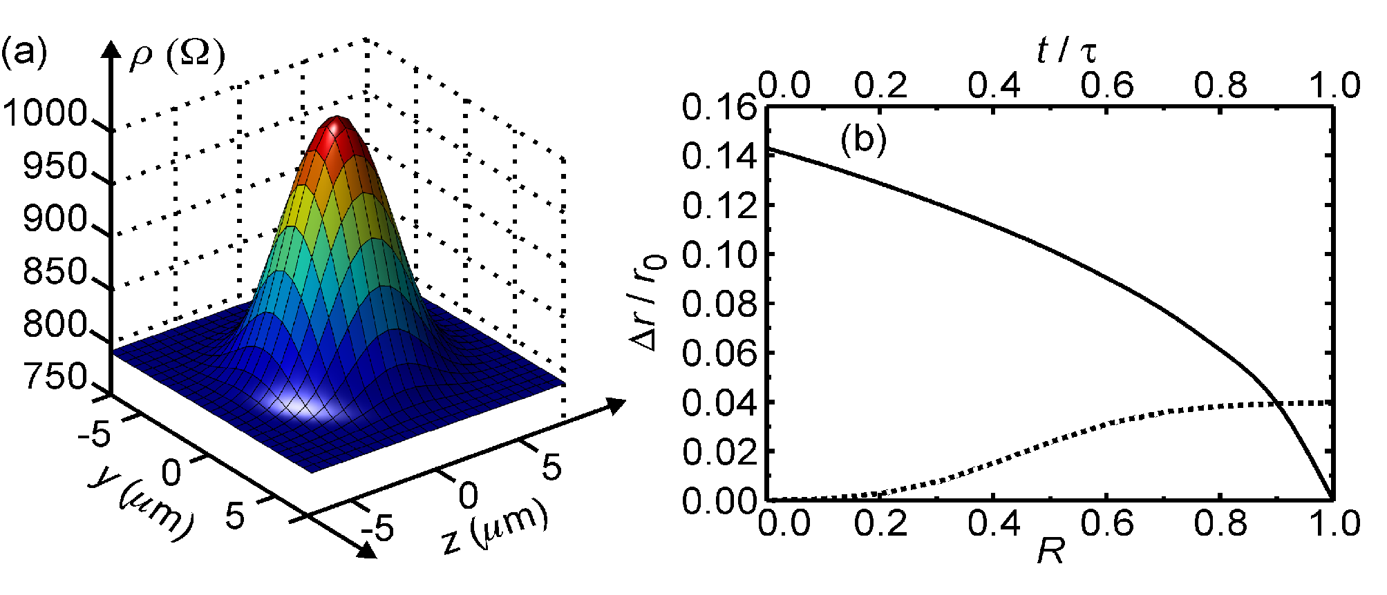
The maximum value that can be measured for the BEC corresponds to the deposition of only atoms. Since this detection threshold is so low, real-time measurements of versus can probe most of the quantum reflection process. To illustrate this, the dotted curve in figure 3(b) shows calculated versus (upper horizontal axis) for , where is the approximate duration of the reflection process, with . For all values in this range, exceeds the threshold required for experimental detection.
The ability to quantify the number of atoms lost as a function of time during a single quantum reflection event is a key advantage of the electrical measurement scheme that we propose. In previous optical measurements, the time evolution of the reflection process could only be inferred by repeating it many times and imaging the BEC slightly later in each successive run Pasquini et al. (2004, 2006). It may also be possible to probe the reflection dynamics spatially by imprinting an array of nm-scale quantum wires in the graphene membrane, either by etching them or by using local hydrogenation to produce insulating regions between adjacent conducting wires Elias et al. (2009). Measuring the resistance changes of each quantum wire during quantum reflection would yield spatio-temporal information about the build-up of adsorbed, and hence non-reflecting, atoms on the graphene surface. Resistance-based measurement may be particularly helpful at low velocities since the formation of solitons and vortices in BECs can make accurate determination of via absorption imaging difficult Scott et al. (2005).
The change in resistance is most conveniently determined using a small () AC drive voltage at 200 kHz and measuring the resulting current. The drive frequency is much greater than the inverse reflection time. This prevents the fields due to the current influencing the potential landscape because the field has zero mean on the time scale of the reflection process. In addition, the peak change in potential energy m from the surface would be J, much less than the atomic energy. Atoms in states might be used since they are insensitive to magnetic fields.
Our model should be checked experimentally by comparing the electrical resistance measurements with atom density profiles obtained from optical absorption images. This could be done by moving a cloud of known atom number and density profile slowly against the graphene until all atoms are adsorbed. The measured resistance change could then be checked against our prediction without needing to image the cloud after interaction with the surface. Since there are no free parameters in our model, a disagreement would lead us to the important conclusion that our understanding of the effect of impurities on graphene is incomplete. Conversely, agreement would validate our claim that resistance measurements can be used to measure reflection probabilities without the use of absorption images.
IV Quantum and Classical Reflection from Semiconductor Heterostructures
Although we have identified ways to increase quantum reflection probabilities to , to create ideal atom mirrors the action of the surface must be altered to enable classical reflection of the atoms. Classical reflection from surfaces such as glass prisms has been successfully enhanced by using evanescent waves Bender et al. (2010). It has also been demonstrated for BECs by using light and magnetic fields Bongs et al. (1999); Arnold et al. (2002); Günther et al. (2007) to create the potential barrier. In the latter case, a wire array was used as a magnetic mirror. Conventional wires are simple and cheap to make but suffer from Johnson noise Wang et al. (2004); Henkel et al. (1999), which causes severe atom losses from BECs near surfaces due to atomic spin flips Fortágh et al. (2002); Estève et al. (2004). Here we show that quantum reflection may be enhanced by using buried wire arrays carrying extremely low current. If 100% reflection can be achieved with currents A, the array can be realised using a two-dimensional electron gas (2DEG) in a semiconductor heterostructure [figure 1(b)]. Such electron gases have considerably lower Johnson noise than metal wires, owing to fewer defects and higher resistance to thermal currents Crell et al. (1997); Wieck and Ploog (1992); Többen et al. (1995). Using ion implantation, a high-quality 2DEG wire array can be constructed only nm below a solid surface [figure 1(b)]. This allows cold atoms to approach very close to the conducting elements, thereby strengthening the atom-solid coupling and increasing the performance of such hybrid devices Judd et al. (2010). Metal wire arrays, fabricated on a chip surface, have already been shown to increase reflection of BECs from surfaces Günther et al. (2005), but their full potential and implementation in 2DEGs has yet to be realised.
The magnetic field magnitude at distance from the 2DEG plane is given approximately by where is the spatial period of the array and m is the distance from the 2DEG to the heterostructure surface [figure 1(b)]. This exponential relation holds provided . We choose to ensure that the reflecting atoms encounter an almost flat magnetic potential (at , the magnetic potential is strongly corrugated). It is important to ensure that is as large as possible, subject to the requirement that it remains small enough to not significantly corrugate the potential parallel to the surface, since the strength of the potential decreases exponentially as is reduced. If small corrugations in the potential can be tolerated, larger values may be chosen. A 2DEG size on the order of mm by mm, along with the grating period of 5m, would be large enough to allow the simple exponential description of the potential. See reference Günther et al. (2011) for further design details.
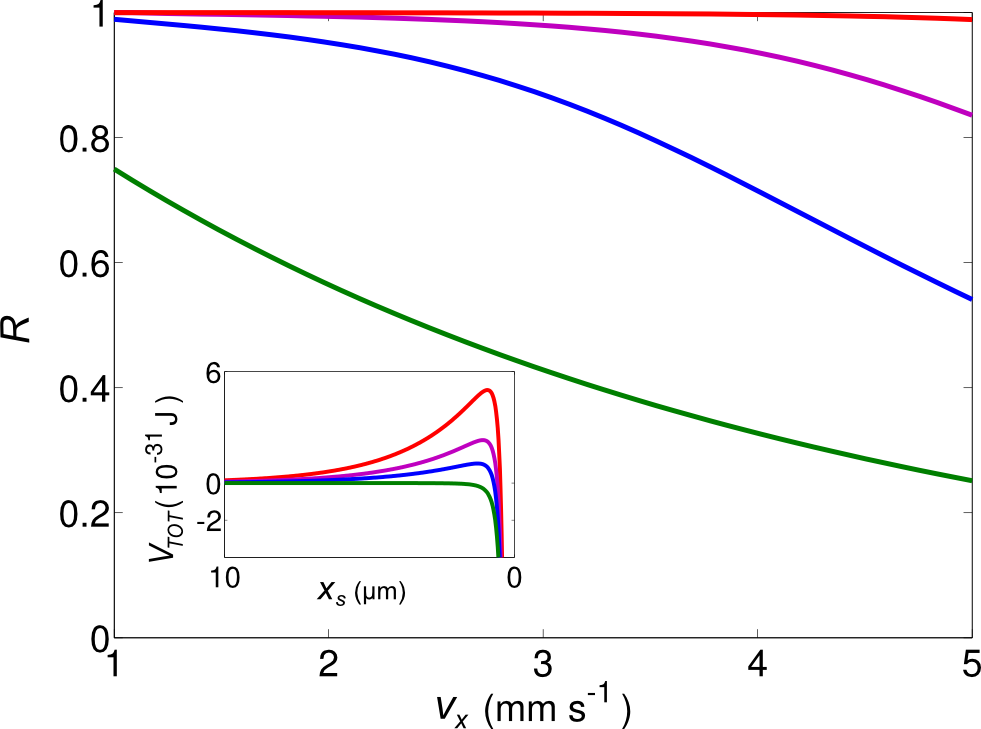
The potential energy of an atom due to the magnetic field may be written where defines the electronic spin state and is the Landé -factor. The exponential decay of occurs on a length scale , comparable with the decay length of the CP potential. Consequently, for sufficiently high the wire array creates a sharp potential barrier. In this regime, the magnetic potential can be combined with to create a rapidly varying total potential energy, which first increases sharply with increasing , attains a positive maximum, and then falls to zero over a few micrometres [figure 4, inset]. This means both quantum and classical reflection can occur.
To demonstrate the effect of the 2DEG current on , we calculate for 7Li plane waves reflecting from bulk GaAs [, J m4] using the transfer matrix method, but now including for -A foo (b). The green curve in figure 4 (bottom) shows calculated for bulk GaAs with as a reference. Figure 4 shows that increasing to A (blue curve, 2nd from bottom) and A (magenta curve, 2nd from top) increases by raising the classical barrier in [figure 4, inset]. At A (red curve, top) the barrier is large enough to produce almost 100% reflection over the entire range of .
Since the values that we consider are low enough to be implemented with standard 2DEGs, the proposed scheme offers a practical route to achieving 100% reflection using well established technology. In addition, because the 2DEG is integrated within the surface, it does not degrade or disrupt the surface, unlike metal surface wires. Small current components across the 2DEG wires, originating from inhomogeneity of the ionised donor distribution, can cause fluctuations in the magnetic field component along the wires. To exponentially suppress such fluctuations, the donor density should be periodically modulated perpendicular to the wires either by optical illumination or by etching narrow (10’s of nm) insulating stripes along them Sinuco-León et al. (2011).
V Conclusions
We have shown that atomic quantum reflection probabilities can be increased to , for typical experimental values, by reducing the thickness of the dielectric substrate and, hence, weakening the CP potential. We have also studied quantum reflection from a suspended graphene monolayer and found that the reflection probabilities exceed those of a bulk dielectric but not those of a nm dielectric film, due to graphene’s high electron mobility and, hence, stronger CP potential. We have explicitly confirmed predictions that a quantum reflection experiment could be used to distinguish between different models for electron behaviour in graphene Churkin et al. (2010). We have identified two key advantages of suspended graphene membranes for quantum reflection studies. Firstly, adsorbed alkali atoms can be removed between successive experimental runs by current annealing, thus diminishing the influence of polarized adsorbates on the atoms’ potential landscape and reflection probability. Secondly, resistance changes produced by the adsorbed atoms provide a non-invasive real-time route to quantifying the complex spatio-temporal dynamics of quantum reflection. High levels of adsorption might make graphene a better atom reflector than the nm glass film since the adsorbates increase the resistance of the sheet and, hence, weaken the potential.
Finally, we have demonstrated that semiconductor heterostructures containing an embedded 2DEG can make perfectly-reflecting atomic mirrors, which should be effective not only for Li but also for heavier atoms, such as commonly-used Rb. Such structures offer exciting possibilities for creating new hybrid quantum systems in which cold atoms couple to solid state devices.
We gratefully acknowledge support from the BW RiSC Programme, the DFG through SFB/TRR21, EPSRC and BW-grid computing resources.
References
- Bongs et al. (1999) K. Bongs, S. Burger, G. Birkl, K. Sengstock, W. Ertmer, K. Rzążewski, A. Sanpera, and M. Lewenstein, Phys. Rev. Lett. 83, 3577 (1999).
- Roach et al. (1995) T. M. Roach, H. Abele, M. G. Boshier, H. L. Grossman, K. P. Zetie, and E. A. Hinds, Phys. Rev. Lett. 75, 629 (1995).
- Bender et al. (2010) H. Bender, P. W. Courteille, C. Marzok, C. Zimmermann, and S. Slama, Phys. Rev. Lett 104, 083201 (2010).
- Judd et al. (2008) T. E. Judd, R. G. Scott, and T. M. Fromhold, Phys. Rev. A 78, 053623 (2008).
- Pasquini et al. (2004) T. A. Pasquini, Y. Shin, C. Sanner, M. Saba, A. Schirotzek, D. E. Pritchard, and W. Ketterle, Phys. Rev. Lett. 93, 223201 (2004).
- Pasquini et al. (2006) T. A. Pasquini, M. Saba, G. Jo, Y. Shin, W. Ketterle, D. E. Pritchard, T. A. Savas, and N. Mulders, Phys. Rev. Lett. 97, 093201 (2006).
- Shimizu (2001) F. Shimizu, Phys. Rev. Lett. 86, 987 (2001).
- Scott et al. (2005) R. G. Scott, A. M. Martin, T. M. Fromhold, and F. W. Sheard, Phys. Rev. Lett. 95, 073201 (2005).
- Churkin et al. (2010) Y. V. Churkin, A. B. Fedortsov, G. L. Klimchitskaya, and V. A. Yurova, Phys. Rev. B 82, 165433 (2010).
- Judd et al. (2010) T. E. Judd, R. G. Scott, G. Sinuco, T. W. A. Montgomery, A. M. Martin, P. Krüger, and T. M. Fromhold, New J. Phys. 12, 063033 (2010).
- Sinuco-León et al. (2011) G. Sinuco-León, B. Kaczmarek, P. Krüger, and T. M. Fromhold, Phys. Rev. A 83, 021401 (2011).
- Bradley et al. (1997) C. C. Bradley, C. A. Sackett, and R. G. Hulet, Phys. Rev. Lett. 78, 985 (1997).
- Pollack et al. (2009) S. E. Pollack, D. Dries, M. Junker, Y. P. Chen, T. A. Corcovilos, and R. G. Hulet, Phys. Rev. Lett. 102, 090402 (2009).
- Cornish et al. (2009) S. L. Cornish, N. G. Parker, A. M. Martin, T. E. Judd, R. G. Scott, T. M. Fromhold, and C. S. Adams, Physica D 238, 1299 (2009).
- Babb et al. (2004) J. F. Babb, G. L. Klimchitskaya, and V. M. Mostepanenko, Phys. Rev. A 70, 042901 (2004).
- Reyes and Eberlein (2009) A. M. Reyes and C. Eberlein, Phys. Rev. A 80, 032901 (2009).
- Scheel and Buhmann (2008) S. Scheel and S. Y. Buhmann, act. phys. slov. 58, 675 (2008).
- Klimchitskaya et al. (2009) G. L. Klimchitskaya, U. Mohideen, and V. M. Mostepanenko, Rev. Mod. Phys. 81, 1827 (2009).
- Bordag et al. (2006) M. Bordag, B. Geyer, G. L. Klimchitskaya, and V. M. Mostepanenko, Phys. Rev. B 74, 205431 (2006).
- Palik (1985) E. D. Palik, Handbook of Optical Constants of Solids (Academic Press Inc., London, 1985).
- Jackson (1975) J. D. Jackson, Classical Electrodynamics (Wiley, 1975), 2nd ed.
- Gilmore (2004) R. Gilmore, Elementary quantum mechanics in one dimension (John Hopkins, 2004).
- Parsegian (2006) V. A. Parsegian, Van Der Waals Forces: A Handbook for Biologists, Chemists, Engineers, and Physicists (Cambridge, 2006).
- Jurisch and Rost (2008) A. Jurisch and J.-M. Rost, Phys. Rev. A 77, 043603 (2008).
- Druzhinina et al. (2010) V. Druzhinina, M. Mudrich, F. Arnecke, J. Madroñero, and A. Buchleitner, Phys. Rev. A 82, 032714 (2010).
- Yu et al. (1993) I. A. Yu, J. M. Doyle, J. C. Sandberg, C. L. Cesar, D. Kleppner, and T. J. Greytak, Phys. Rev. Lett. 71, 1589 (1993).
- Alemán et al. (2010) B. Alemán, W. Regan, S. Aloni, V. Altoe, N. Alem, C. Girit, B. Geng, L. Maserati, M. Crommie, F. Wang, et al., ACS Nano 8, 4762 (2010).
- Barash and Kyasov (1989) Y. S. Barash and A. A. Kyasov, Sov. Phys. JETP 68, 39 (1989).
- Dobson et al. (2006) J. F. Dobson, A. White, and A. Rubio, Phys. Rev. Lett. 96, 073201 (2006).
- foo (a) The weaker potential pushes the quantum reflection zone, where , closer to the surface. This may explain why quantum reflection from aerogels did not produce the theoretically predicted increase of Pasquini et al. (2006). Although the potential is very weak, the quantum reflection zone spans the same length scale as the surface roughness. This probably induces random scattering of the incident atoms (and the photons that create ), thereby reducing .
- Barton (2005) G. Barton, J. Phys. A.: Math. Gen. 38, 2997 (2005).
- Bordag (2006) M. Bordag, J. Phys. A.: Math. Gen. 39, 6173 (2006).
- Blagov et al. (2007) E. Blagov, G. L. Klimchitskaya, and V. M. Mostepanenko, Phys. Rev. B 75, 235413 (2007).
- Bolotin et al. (2008) K. I. Bolotin, K. J. Sikes, Z. Jiang, M. Klima, G. Fudenberg, J. Hone, P. Kim, and H. L. Stormer, Solid State Communications 146, 351 (2008).
- Ohta et al. (2006) T. Ohta, A. Bostwick, T. Seyller, K. Horn, and E. Rotenberg, Science 313, 951 (2006).
- Bostwick et al. (2007) A. Bostwick, T. Ohta, T. Seyller, K. Horn, and E. Rotenberg, Nat. Phys. 3, 36 (2007).
- Choi and Jhi (2008) S. M. Choi and S. H. Jhi, Phys. Rev. Lett. 101, 266105 (2008).
- Hwang et al. (2009) C. G. Hwang, S. Y. Shin, S. M. Choi, N. D. Kim, S. H. Uhm, H. S. Kim, C. C. Hwang, D. Y. Noh, S. H. Jhi, and J. W. Chung, Phys. Rev. B 79, 115439 (2009).
- Jin et al. (2010) K. H. Jin, S. M. Choi, and S. H. Jhi, Phys. Rev. B 82, 033414 (2010).
- Chan et al. (2011) K. T. Chan, H. Lee, and M. L. Cohen, Phys. Rev. B 83, 035405 (2011).
- Adam et al. (2007) S. Adam, E. H. Hwang, V. M. Galitski, and S. D. Sarma, Proc. Natl. Acad. Sci. U.S.A. 104, 18392 (2007).
- Chen et al. (2008) J. H. Chen, C. Jang, M. S. Fuhrer, E. D. Williams, and M. Ishigami, Nature Physics 4, 377 (2008).
- Schedin et al. (2007) F. Schedin, A. K. Geim, S. V. Morozov, E. W. Hill, P. Blake, M. I. Katsnelson, and K. S. Novoselov, Nature Materials 6, 652 (2007).
- Elias et al. (2009) D. C. Elias, R. R. Nair, T. M. G. Mohiuddin, S. V. Morozov, P. Blake, M. P. Halsall, A. C. F. D. W. Boukhvalov, M. I. Katsnelson, A. K. Geim, and K. S. Novoselov, Science 323, 610 (2009).
- Arnold et al. (2002) A. S. Arnold, C. MacCormick, and M. G. Boshier, Phys. Rev. A 65, 031601 (2002).
- Günther et al. (2007) A. Günther, S. Kraft, C. Zimmermann, and J. Fortágh, Phys. Rev. Lett. 98, 140403 (2007).
- Wang et al. (2004) D. Wang, M. D. Lukin, and E. Demmler, Phys. Rev. Lett. 92, 076802 (2004).
- Henkel et al. (1999) C. Henkel, S. Pötting, and M. Wilkens, App. Phys. B 69, 379 (1999).
- Fortágh et al. (2002) J. Fortágh, H. Ott, S. K. Günther, and C. Zimmermann, Phys. Rev. A 66, 041604 (2002).
- Estève et al. (2004) J. Estève, C. Aussibal, T. Schumm, C. Figl, D. Mailly, I. Bouchoule, C. I. Westbrook, and A. Aspect, Phys. Rev. A 70, 043629 (2004).
- Crell et al. (1997) C. Crell, S. Friedrich, H.-U. Schreiber, and A. D. Wieck, J. Appl. Phys. 82, 4616 (1997).
- Wieck and Ploog (1992) A. D. Wieck and K. Ploog, Appl. Phys. Lett. 61, 1048 (1992).
- Többen et al. (1995) D. Többen, D. K. de Vries, A. D. Wieck, M. Holzmann, G. Abstreiter, and F. Schäffler, Appl. Phys. Lett. 67, 1579 (1995).
- Günther et al. (2005) A. Günther, S. Kraft, M. Kemmler, D. Koelle, R. Kleiner, C. Zimmermann, and J. Fortágh, Phys. Rev. Lett. 95, 170405 (2005).
- Günther et al. (2011) A. Günther, T. E. Judd, J. Fortágh, and C. Zimmermann, in Atom Chips, edited by J. Reichel and V. Vuletic (Wiley-VCH, 2011), pp. 171–210.
- foo (b) The electric field due to the voltage applied across the 2DEG can be neglected for the small currents we consider here.