Transport Measurements of Strongly-Correlated Electrons on Helium in a Classical Point-Contact Device
Abstract
We present transport measurements of electrons on the surface of liquid helium in a microchannel device in which a constriction may be formed by a split-gate electrode. The surface electron current passing through the microchannel first decreases and is then completely suppressed as the split-gate voltage is swept negative. The current decreases in a steplike manner, due to changes in the number of electrons able to pass simultaneously through the constriction. We investigate the dependence of the electron transport on the AC driving voltage and the DC potentials applied to the sample electrodes, in order to understand the electrostatic potential profile of the constriction region. Our results are in good agreement with a finite element modeling analysis of the device. We demonstrate that the threshold of current flow depends not only on the applied potentials but also on the surface electron density. The detailed understanding of the characteristics of such a device is an important step in the development of mesoscopic experiments with surface electrons on liquid helium.
pacs:
73.20.-r, 73.23.-b, 85.30.Hi, 45.50.JfI Introduction
An electron close to the free surface of liquid helium is subjected to an attractive force due to a weak image charge formed in the liquidAndrei ; MonarkhaKono . In the presence of an applied electric field , the potential in the direction perpendicular to the helium surface may be written as where , is the dielectric constant of the liquid, is the absolute value of the electronic charge and is the distance from the helium surface. The electron is prevented from entering the liquid due to a eV potential barrier at the surface and so remains localized above the liquid. The potential gives rise to a series of bound states for perpendicular motionGrimesImageStates ; in the ground state, the expectation value of is nm. The lifetime of these bound states is predicted to be long, leading to the proposal that electrons on the surface of liquid helium may be good candidates for quantum bitsPlatzmanandDykmanscience .
For a two-dimensional system of charges on a liquid helium surface, the electron surface density may be varied over a wide range, up to a theoretical limit given by the hydrodynamic instability of the bulk liquid surfaceGorkov ; Leiderer1979189 ; LeidererDimples of 2.2 cm-2. By varying temperature the scattering processes which determine the electron mobility in the plane parallel to the helium surface may be controlled. Below K the density of gas atoms above the liquid surface becomes effectively zero and scattering occurs only with excitations of the liquid surface, ripplons, leading to high mobilitiesShirahamaMobility in excess of 108 cmVs. As the Coulomb interaction between electrons is essentially unscreened, and the electron separation is much larger than the thermal electron wavelength, SSE have been used to study classical effects in strongly-interacting electron systems, such as the transition from an electron liquid to a 2D Wigner solid as the temperature of the electron system is decreasedGrimesAdamsWignerCrystal .
Quasi-one dimensional SSE systemsKovdryaReview have been investigated using samples in which liquid helium was confined in grooves on a dielectric substrateKovdryaNikolaenko . The width of the grooves was as low as 1.25 m. In such experiments, the temperature dependence of the electron mobilityKovdryaNikolaenko2 was found to be in good agreement with that predicted by theoretical calculations where transitions between quantized energy levels for the lateral motion of the electrons were taken into accountSokolov1Dmobility . However, for such dielectric substrates the mobility was also dependent on substrate defects in regions where the helium film was thin.
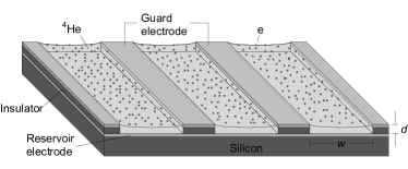
Recent experiments have made use of microchannel devices fabricated by lithographic techniques in order to study the properties of SSE in confined geometries. A schematic representation of a set of such microchannels is shown in Fig. 1. Placed a distance above the bulk surface of superfluid helium, the channel will fill by capillary action; the helium surface may then be charged. The radius of curvature of the liquid is given by where and are the surface tension coefficient and density of liquid 4He respectively, is the acceleration due to gravity and is the dielectric constant of vacuumMartyCurvature . The transport of electrons in such devices was first demonstrated for a channel of width 30 m and depth 1 mvanHaren . The non-linear transport of the Wigner solid on helium surfaces in microchannels of width 8-20 m was studied in three-terminal devices comprising of source, drain and gate electrodes submerged beneath the helium surfacePhil'sChannels ; IkegamiWigner . The ultra-efficient transfer of a small number of electrons along parallel microchannels of width 10 m, again using a series of gate electrodes beneath the helium surface, has also been demonstratedsabouret . In still more advanced devices, small ensembles of electrons, including a single electron, trapped in a microfabricated circular pool of radius 10 m, have been studied using a charge-sensitive superconducting Single Electron Transistor (SET) positioned beneath the helium surfaceCountingElectronsOnLHe . A Field Effect Transistor (FET) for electrons on a thin helium film, where the electron density may exceed the hydrodynamic limit, has also been demonstratedheliumFET . There the separation between the split-gate electrodes was 200 m.
Such experiments demonstrate a progression towards the sensitive control and measurement of small numbers of SSE on helium, raising the possibility of studying novel phenomena associated with classically interacting charge systems in confined geometries. Many theoretical studies have been conducted on the behavior of such systems. In quasi-one dimensional systems, at sufficiently low temperatures, particles are predicted to form a series of rows, the number of which changes with the particle density or confinement strength, leading to structural phase transitions and re-entrant melting processesChaplik ; Peeters1DCrystal . Similar phenomena have also been predicted in circularly symmetric parabolic confinementsbedanov . The pinning and depinning dynamics of charged particles at potential constrictions have also been investigated using Monte Carlo calculationsPeetersConstriction ; daSilvaPinning ; damascenoPinning . However, experimental difficulties have restricted progress towards investigating these phenomena. SET charge measurements, whilst extremely sensitive, may be plagued by intrinsic two-level fluctuator charge noiseZimmerman ; reesSCPT . Also, the electrostatic potential profile in microchannel devices may be distorted by contact potentials and surface charging effects which can be difficult to quantifymukharsky .
As a step towards overcoming these experimental difficulties, we have performed transport measurements of SSE on superfluid 4He in a microfabricated device. In this sample, two microchannel SSE reservoirs are separated by a split-gate electrode which, at appropriate bias, forms a constriction. As the split-gate voltage is swept negative the current I flowing through the constriction is reduced and then reaches zero at a threshold voltage . The appearance of step-like decreases in current in this device, where each step corresponds to a change in the number of electrons able to pass simultaneously through the constriction, has already been reportedReesprl . Here we present further transport measurements, investigating in particular the response of the system to increasing AC driving voltage, which causes significant non-linear transport effects to emerge. These results are discussed in relation to an electrostatic model of the sample which shows that offsets in electrode potentials, arising for reasons which are not yet clear, are important in determining the potential profile of the device.
II Experimental
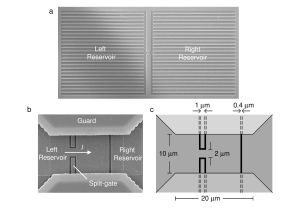
The sample used in this experiment was prepared using multilayer optical and electron-beam lithography on a Si wafer, the surface of which was oxidized. Two arrays of microchannels, defined by a guard electrode, act as electron reservoirs between which electrons may be exchanged. These left and right reservoirs consist of 25 microchannels of width 20 m arranged in parallel and connected together at one end (Fig. 2(a)). The two reservoirs are separated by a smaller channel of width 10 m and length 20 m. Electrodes were fabricated beneath the reservoir microchannels and are denoted as the left and right reservoir electrodes respectively. A split-gate electrode was fabricated at the base of the small central channel (Fig. 2(b)). The geometry of the central channel is shown in Fig. 2(c); the split gate was 1 m long and separated by a gap of 2.8 m. The 400 nm gap between left and right reservoir electrodes was placed 10 m to the right of the split gate in order to avoid the distortion of the potential profile of the constriction region. A 1.5 m thick layer of hard baked photoresist, which defined the microchannel depth , separated the lower electrodes from the guard electrode. All metal layers were made of gold (65 nm thick) on top of a thin (15 nm) titanium layer which was deposited in order to promote adhesion.
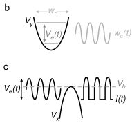
The sample was placed in an experimental cell approximately 0.5 mm above the bulk surface of superfluid 4He at 1.25 K. The potentials , and were applied to the guard, reservoir and split-gate electrodes, respectively. Under the bias conditions = 0 V, V, the surface of the helium was charged by thermionic emission from a small tungsten filament placed a few mm above the sample. A small AC voltage of frequency 200 kHz was superimposed on the right reservoir electrode in order to drive electrons between the two reservoirs, through the central channel. The current I and conductance of the electron system G were determined by making a phase-sensitive measurement of the voltage capacitively induced on the left reservoir electrode, in reference to the standard lumped-circuit modelIye .
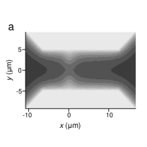
To aid the understanding of the electrostatic potential profile of the device, a finite element model of the central channel was developedFlex . The results of the modeling are shown in Fig. 3(a) for V, V. When is more negative than , a saddle-point potential is formed on the helium surface at the point (), with a maximum in potential for electrons in the x direction along the channel and a minimum in the lateral y direction. Fig. 3(b) shows how the potential profile develops as is changed. For -2.3 V the potential at the center of the saddle-point is more negative than the guard electrode potential. We assume that the electrostatic potential energy of the electron system may not exceed , as this would lead to electrons escaping from the reservoirs, onto the thin helium film covering the guard electrode, through which they should rapidly drain awayLeidererThinFilm . Therefore, when the potential at the center of the saddle-point is more negative than the guard electrode potential, the resulting potential barrier between the two reservoirs should block electron transport through the constriction.
III Results and Discussion
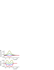
Before discussing experimental results, we first develop an electrostatic model of the device, following the approach presented previouslyReesprl . Note that in this model, a more positive voltage corresponds to a lower potential energy for an electron. We estimate that the change in the depth of the helium at the center of the 20 m-wide reservoir microchannels should be less than 0.1 m. Therefore we do not take the curvature of the helium surface into account here. We begin by assuming that the electron system may be considered as a charge continuum. The electrostatic potential energy of the electron system in the reservoirs, , depends on the reservoir electrode voltage and the electron density. Therefore we may write . The results of the finite element modeling analysis (Fig. 3) indicate that a saddle-point potential is formed at the constriction between the two reservoirs when is more negative than . At appropriate values of a potential barrier between the two reservoirs may be formed. The saddle-point potential may be written as where is the potential at the center of the saddle-point and and are constants. We consider that for electrons may pass over the potential barrier, allowing transport through the constriction, whereas for electron transport is blocked. The condition therefore defines the threshold of current flow through the constriction. This condition is depicted schematically in Fig. 4(a).
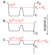
The influence of the reservoir, split-gate and guard electrodes on the potential barrier may be estimated by considering the region of space at the center of the constriction to have some capacitance to the three electrodes, , and , as well as a stray capacitance to the surroundings . The total capacitance of the region is then described by and we can define constants to represent the relative strength of coupling from each electrode to the barrier region as , , and . Experimentally it was found that, on increasing and by +100 mV simultaneously the threshold of current flow also increased by exactly +100 mV (data not shown), indicating that was in fact negligibly small () and that . The potential at the center of the constriction may then be written as .
We now consider the case in which the reservoir voltage is set progressively more negative with a fixed bias applied to the split gate and guard electrode (here we assume to be small). This is depicted schematically in Fig. 4(a-c); from top to bottom goes from positive to negative bias. In Fig. 4(a) we see that, at a certain positive reservoir bias, the height of the potential barrier just meets the potential energy of the electron system and the current is ‘pinched-off’. Making more negative (Fig. 4(b)) causes both and to become more negative. As remains below the guard potential electrons do not escape from the channels onto the thin helium film above the guard; there is no change in the electron density and simply changes by the change in . However, the change in the barrier height is smaller due its additional dependence on the split-gate and guard electrodes (). Therefore a negative change in causes to become more positive relative to and current flows across the barrier. By setting more negative still (Fig. 4(c)) electrons are eventually lost to the guard leading to a reduction in until is equal to the guard potential. Now as becomes more negative, becomes more negative with respect to and the current may eventually be suppressed once more.
We denote the value of for which as . Following the model described above, expressions may now be derived to describe the dependence of on , for constant . From the threshold condition , for the case where we have
| (1) |
and for the case where ,
| (2) |
Rearranging (1) and (2) gives respectively,
| (3) |
and
| (4) |
Because the separation between the split-gate electrodes (2.8 m) is comparable to the inter-electron spacing ( m for cm-2), we expect only a small number of electrons to be in the constriction region when the system is close to the threshold condition. To estimate this number, we model the center of the constriction as a small square of area , where is the effective width of the constriction. As the FEM calculation indicates that the constant is small compared to , we will assume that the potential in the direction is flat, whilst the electrons are confined in the direction by a parabolic potential , as pictured schematically in Fig. 4(d). The maximum lateral displacement for electrons in the constriction, , satisfies the expression . Substituting gives
| (5) |
Note that for the threshold condition , . Assuming a parallel-plate capacitor approximation, the charge density in the area may be written as
| (6) |
and the total number of electrons in is therefore
| (7) |
After integration over the limits as given by Eq. (5), we obtain the result
| (8) |
Although for the electron liquid electrons are not localized as in the Wigner crystal, we assume that electrons are distributed evenly over , effectively forming a series of rows across the constriction. The number of electrons lying in the direction across the constriction may then be estimated as . For constant and , we also have the relation . This gives an expression relating to as
| (9) |
The number of electrons across the constriction should therefore increase linearly with increasing above the current threshold.
We suggest that the granularity of charge may cause some deviation from the behavior of the system as expected under the charge continuum model. From Eq. (9), the value of for which one row of electrons may be formed in the constriction () is
| (10) |
For the number of electron rows across the constriction is less than 1. Therefore, as no electrons are present in the constriction, current flow should be suppressed when rather than at the threshold condition assumed under the charge continuum model . We may now correct Eqs. (3) and (4) to give for changing at constant . For the case where we have
| (11) |
and for the case where ,
| (12) |
Note that the value of , which describes the parabolic lateral confinement at the constriction, is dependent on the potential applied to the reservoir electrodes (assuming constant ). The FEM calculation of the potential profile shows this dependency to be linear. The corrective terms therefore introduce a non-linear dependence of on . However, in the following discussion, we will assume that, for constant , small changes in cause a negligibly small change in .
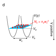
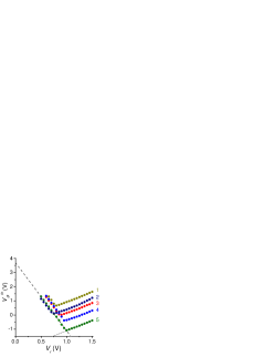
We have performed measurements in order to determine whether the charge continuum model or the granular charge model best describes the dynamics of electrons in the device. We denote the experimentally determined value of the split-gate voltage for which the current is suppressed as . Figure 5(a) shows the dependence of the current I flowing through the central channel as is varied for different values of the driving voltage . The current decreases as is swept negative and finally is completely suppressed at the threshold voltage , which for all cases is more negative than the reservoir voltage V. The linear dependence of on is shown in Fig. 5(b). The threshold for current flow occurs at more negative split-gate bias as the driving voltage is increased.
Measurements of SSE current flow over a potential barrier formed by a split-gate electrode in a similar device have already been reportedourJLTP . There, for values of up to 100 mVpp, it was shown that current flow across a potential barrier could be induced by increasing until the potential energy of the electron system could overcome the barrier, allowing electrons to be transferred between the reservoirs. Here we observe the same behavior. The dependence of on is discussed in more detail later in this section.
In Fig. 5(c) we show the corresponding conductance G for each current measurement. Above , G increases sharply for all values of . Considering the saddle-point potential shown in the modeling results in Fig. 3, both the depth of the potential at the center of the constriction (which is proportional to the electron density in the constriction under the charge continuum model), and the effective width of the constriction, should increase as is swept positive. Both effects should lead to an increase of conductance at the constriction. For high values of , where the split-gate electrode is more positive than the reservoir electrode and no potential barrier is expected to exist, G rises further, presumably due to the continuing increase of the electron density in the constriction region.
For still higher values of , the conductance eventually saturates. For mVpp, M at V. As the total conductance of the electron system no longer depends on the split-gate voltage in this region, we assume that the resistance of the constriction region is small compared to that of the electron system in the reservoirs. Therefore, the saturated conductance can be attributed to that of the reservoir region, and by subtracting the value of the resistance at this split-gate voltage, M, from the values of the resistance over the entire split-gate sweep, an approximation of the constriction resistance can be calculated. The corresponding conductance of the constriction, , is shown in Fig. 5(d), for mVpp. We see that above the conductance threshold, increases in a series of steps. The steps are not a series of sharp rises and flat plateaus; rather, they appear smoothed-out. We add to the plot a guide to the eye (grey dotted line) indicating the manner in which a sharp step pattern fits the data. We align each sharp step with the maximum in the gradient at each increase in . The spacing between the steps is mV.
We suggest that the increasing number of electron rows across the constriction could lead to steplike increases in the constriction conductance. Such behavior is observed in other classical many-body systems with long-range interactions, such as pedestrians moving through bottlenecksHoogendoorn2005 . Here, such an effect is essentially the result of Coulomb blockade at a single constriction; for the case in which and one electron row occupies the constriction, Coulomb repulsion prevents other electrons from passing through and electrons may only pass through in a single row. As the constriction is opened to the point where , the additional conduction channel should cause an increase in the constriction conductance as electrons may now pass freely through the constriction, side-by-side. The steplike increase in conductance resembles the quantized conductance steps observed in quantum point contact devicesOriginalQPC . From the FEM calculation results shown in Fig. 3(b), we estimate that the spacing of the energy subbands for lateral motion at the constriction to be meV, which, as shown below, is much smaller than the change in associated with each conductance step, and is also smaller than . We therefore conclude that the origin of the steps observed here, due to the Coulomb interaction between electrons at the constriction, is quite different to the case of the quantum point contact, of which our device acts as a classical analogue.
The smoothing of the steps in indicates that neither the charge continuum model, nor the granular charge model, describes the system precisely. We assume that the sharp steps fitted to the data in Fig. 5(d) correspond to the values of where, under the granular charge model, the number of electrons able to pass simultaneously through the constriction increases by 1. By extrapolation of these fitted steps, we can obtain an estimate of V. As described above, the constriction conductance should increase with increasing and as becomes more positive. The FEM calculation shows that whereas . We therefore naively expect the conductance of the constriction to vary as , under the charge continuum model. In Fig. 5(d) we plot the function (solid grey line). We see that this function describes reasonably well, other than at points along the curve where the conductance is suppressed, which we attribute to deviations from the continuum model due to the granular nature of charge. The agreement becomes closer for higher values of as the step features are lost, presumably as the number of electron rows increases and the electron system at the constriction better approximates a 2D charge continuum. We therefore conclude that whilst the granularity of charge causes observable deviations from the charge continuum model, and causes the current to be suppressed above the expected threshold , the simplified approach depicted in Fig. 4(d) does not describe the system accurately. Correspondingly, the experimentally observed threshold of current flow, V, lies between the values which we have estimated correspond to and .
We suggest that our experimental observation of the step-like increase in the conductance of the constriction may be verified by molecular dynamics simulations of classical charge systems at potential bottlenecksPeetersConstriction . Indeed, recent simulations of a system very similar to ours reproduce the smooth steplike increase in , and show that each step is related to an increase in the number of electron rows across the constrictionAraki2011 . These simulations also indicate that temporal fluctuations in the potential of electrons at the constriction, which are of thermal origin but essentially due to electron-electron interactions, and are not considered in our mean-field approach, cause the smoothing of the conductance steps. These fluctuations also cause to lie at vales of more negative than as, even for the case , there still exists some probability that the potential of electrons may be raised in order to overcome the barrier at the constriction, thus allowing transport. For our experiments, the driving voltage causes an additional modulation of the electron density at the constriction over each AC cycle. In Fig. 5(c) the smoothing of the step-like features increases with increasing , as discussed in more detail later in this section. However, we note here that extrapolation of the data shown in Fig. 5(b) to the limit mVpp yields a value of V, which is a small change from the value recorded for mVpp and is still more negative than the value of V. Further comparison of our experimental results with numerical simulations is required to fully understand the dynamics of the electron system close to the conductance threshold.
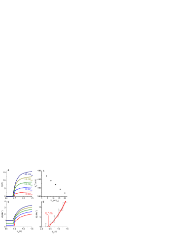
We consider that the modulation of the potential of the electron system due to the applied driving voltage may cause additional non-linear behavior to appear in the electron transport properties close to the current threshold. To investigate such effects, the magnitude of the second harmonic component of the AC voltage induced on the left reservoir electrode, , was measured. In the case that the SSE AC current flow is perfectly sinusoidal in response to the driving voltage, the second harmonic component is zero. However, if the conductance should vary over each AC cycle, the current signal should become distorted causing higher frequency components to appear. In Fig. 6(a) we see that indeed rises as is swept negative and reaches a maximum close to . The magnitude of increases with the driving voltage .
In Fig. 6(b) and (c) we depict schematically two processes which may give rise to the distortion of the electron current through a saddle-point potential as the electron energy is modulated. In the first case (Fig. 6(b)), when is close to the bottom of the parabolic potential , the effective width of the conductive channel changes over the AC cycle which should lead to a time dependence of the conductance G. In addition, the effective depth of the potential for electrons at the constriction also varies, which should lead to a variation of the electron density, and so conductance, over each cycle. In the second case (Fig. 6(c)), as the potential maximum in is raised and becomes higher than , electrons are expected to flow only intermittently across the barrier.
In both of these cases, the degree of distortion in the current should reach a maximum close to the threshold of current flow. We therefore find the observed increase in close to the current threshold to be consistent with transport through a saddle-point potential. We also note that appears to rise in a series of weak peaks or steps which appear to mirror the step-like decrease in conductance observed in Fig. 5(c). We again find this to be consistent with our model. For values of where is large, modulating gives rise to a large change in conductance over each AC cycle, and so the value of should be large. Each step in conductance should therefore be accompanied by a peak in . Indeed, the step-like feature in the conductance at V (Fig. 5(c)) is accompanied by a weak second peak in at the same split-gate voltage. However, the non-linear response of the SSE system to a driving field has been predicted by Saitohsaitoh and observed experimentallybridges . We therefore note that the distortion in the current signal may also be due in some part to the intrinsic non-linear transport properties of the SSE system rather than solely due to the geometry or potential profile of the device.
The dependence of on was investigated by measuring the current threshold for decreasing values of , from 1.5 V to 0 V in 50 mV steps, for mVpp. The results of 5 such measurements, taken on different days, are shown in Fig. 7. In all 5 cases the split-gate voltage required to suppress the current initially becomes more negative as the reservoir potential is made more negative. Then, at a certain reservoir potential, the trend is reversed; the threshold moves to more positive values as the reservoir potential becomes more negative. In both cases the relationship between and is approximately linear. These results are found to be in agreement with the behavior predicted by our electrostatic analysis. Starting at highly positive reservoir electrode bias, must initially be made more negative to suppress the current flow each time is set more negative, to compensate for the reduction in the barrier height relative to . Then, as electrons are lost to the guard, decreases and remains constant, the split-gate voltage must be made more positive to allow current flow with each step in , due to the relative increase of the barrier height. The intersection between the two linear regions in the data marks the point at which electrons begin to escape to the guard. This point is different for each data set indicating that the initial surface density in each case was different. The intersection was not observed to occur for values of greater than +1.0 V, the voltage at which the electron reservoirs were charged.
By making linear fits to the data presented in Fig. 7, we may derive values for , and based on the charge continuum model, using Eqs. (3) and (4), and the relation . The values of the coupling constants were determined for each of the data sets. The similarity in the gradient of each data set indicates the stability of the coupling constants, the average values of which are shown in Table 1.
We may also estimate , and taking into account the fact that the experimentally determined current threshold does not correspond exactly to . The results in Fig. 5 show that appears to lie closer to , the threshold under the granular charge model, as given by Eqs. (11) and (12). Whilst the constant , which determines the deviation of from , may be estimated from the FEM modeling of the device, here we adopt a more straight-forward approach to take into account the deviation of from . From Fig. 5, for V, V. As discussed in more detail below, the reservoir electrode potential is equal to the guard electrode potential for V, due to an offset in the potential of the guard electrode. Because no parabolic confinement exists when , for this condition we expect and therefore V. As the correction to should display a square-root dependence on , the value of can be estimated for each value of using the expression
| (13) |
The average values for , and calculated using the values for given by Eq. (13) are also listed in Table 1.
The coupling constant may also be estimated from dependence of on shown in Fig. 5(b). We assume that, on increasing , the increase in the barrier height required to suppress the current is equal to the corresponding increase in the maximum energy of the electron system in the right reservoir, . Because, for fixed bias on the reservoir and guard electrodes, we may derive from the gradient in Fig. 5(b) as . Similar measurements were made by sweeping the reservoir and guard potentials (data not shown) in order to determine the dependence of the thresholds and on . Under the charge continuum model, the constants and may be given by and . The results of these measurements (denoted ) are shown in Table 1 as well as the corresponding values calculated from the finite element model.
| Coupling constant | Calculated (FEM) | Measured (Eqs. (3), (4)) | Measured (Eq. (13)) | Measured () |
|---|---|---|---|---|
| 0.75 | 0.77 | 0.79 | 0.83 | |
| 0.10 | 0.16 | 0.15 | 0.10 | |
| 0.15 | 0.07 | 0.06 | 0.07 |
From the results shown in Table 1, we see that, compared to the values calculated using Eqs. (3), (4), the change in , and when including the correction given by Eq. (13) is small. These values are also close to those given by measuring the dependence of on . All the experimentally determined values are in relatively good agreement with the FEM calculation. For all four results, is largest and so the reservoir electrode dominates in determining the height of the potential barrier. This confirms that in our experiment, close to the conductance threshold, the electrons are indeed passing through the region between the split-gate electrodes and above the reservoir electrode.
The determination of the constant allows the expected change in to add one electron row across the constriction to be calculated using Eq. (10). We use the FEM model to obtain an estimate of Vm-2 for V and =0.62 V. Using we find that mV. This value is in good agreement with the experimentally observed step separation, mV for V (Fig. 5(d)), indicating that the step-like increases in are indeed due to increases in the number of electrons across the constriction. The change in split-gate voltage is related to the corresponding change in by the constant . For , mV, which is comparable to . We therefore conclude that the increase of smoothing of the steplike features with increasing may be due to the modulation of the electron density at the constriction, which causes transport features arising from the discreet number of electrons across the constriction to be lost.
The data shown in Fig. 7 was taken with a voltage of V applied to the guard electrode. From Eq. (4) it is then to be expected that V for V. However, the intercept on the axis for each data set is typically +3.6 V indicating a true value of the guard potential of V. This apparent offset is confirmed experimentally for each of the data sets; below a value of V the electron signal was lost completely indicating that at this point . The offset is seen to vary over a small range; for data sets with a higher intercept on the axis the electrons were lost at more positive values of . Despite thermally cycling the device to room temperature and making efforts to ensure correct grounding of the experimental wiring the offset remained. However, the stability of the offset over many hours or days allowed consistent measurements to be made. Voltage offsets in mesoscopic devices may be caused by contact potential differences, thermoelectric effects or surface charging effectsmukharsky . The cause of the offset observed in this experiment is not yet clear. Taking the offset into account, the estimated initial surface electron densities for the data sets 1-5 shown in Fig. 7 are 0.70, 0.50, 0.99, 1.28, cm-2 respectively.
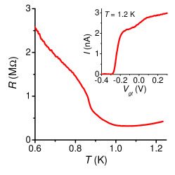
The melting temperature of the 2D Wigner solid depends on the electron density as Phil'sChannels . For the case of a potential offset on the guard potential of +0.62 V, the saturated electron density achieved when charging the reservoirs with V is cm-2 which gives a value of K. In Fig. 8 we show the temperature dependence of the resistance of the electron system for V. At 1.23 K the current threshold was measured (inset). In reference to Fig. 7, the highly negative value of the threshold V indicates that the density was close to saturation. The increase in below 1 K is attributed to the formation of the 2D Wigner solid. The localization of electrons in the Wigner lattice leads to the formation of a small depression, or dimple, in the helium surface beneath each electron, which increases the electron effective mass, and so resistivity of the systemShikinMonarkhaDimples . Recent experiments have investigated the transport of the Wigner solid in a microchannel geometry where the decoupling of the electron lattice from the dimple lattice at high driving fields leads to a highly non-linear responseIkegamiWigner . In our measurement, a sharp increase in the resistance is observed at K which may correspond to the melting temperature of the electron system, in agreement with the predicted value of for the case in which the guard potential is offset.
IV Conclusions
We have investigated the AC transport of strongly-correlated electrons on the surface of liquid helium at a constriction formed by a split-gate electrode. The electron current may be suppressed by sweeping the voltage of the split gate negative. The threshold for current flow was dependent on the DC voltages of all the device electrodes and the AC driving voltage applied to the electron system, as well as the electron density. Step-like increases in the conductance of the electron system as the split-gate voltage was swept positive were found to be due to increases in the number of electrons able to pass simultaneously through the constriction. The device therefore acts as a classical analogue of the quantum point contact. Our results are in good agreement with a simple model of the device developed with the aid of finite element analysis software in which a saddle-point potential profile is formed at the constriction. Comparison with this model reveals that a potential offset on the guard electrode of the device plays a crucial role in determining the potential profile of the sample. Such detailed characterization of microfabricated samples for electrons on the surface of liquid helium is an important step towards the realization of more advanced mesoscopic devices such as single electron devices and quasi-one dimensional wires.
Acknowledgements.
We thank M. Dykman, F. Nori, K. Ono, H. Totsuji, M. Araki and H. Hayakawa for useful discussions. This work was partially supported by Kakenhi. DGR was supported by the RIKEN FPR program.References
- (1) E. Andrei (ed.), Two-dimensional electron systems on helium and other cryogenic substrates. (Kluwer Academic, Dordrecht, 1997)
- (2) Y.P. Monarkha, K. Kono, Two-Dimensional Coulomb Liquids and Solids (Springer-Verlag, Berlin, 2004)
- (3) C.C. Grimes, et al., Phys. Rev. B 13(1), 140 (1976)
- (4) P.M. Platzman, M.I. Dykman, Science 284, 1967 (1999)
- (5) L. Gor’kov, D. Chernikova, JETP Lett. 18(2), 68 (1973)
- (6) P. Leiderer, M. Wanner, Phys. Lett. A 73(3), 189 (1979)
- (7) M. Wanner, P. Leiderer, Phys. Rev. Lett. 42(5), 315 (1979)
- (8) K. Shirahama, S. Ito, H. Suto, K. Kono, J. Low Temp. Phys. 101, 439 (1995)
- (9) C.C. Grimes, G. Adams, Phys. Rev. Lett. 42(12), 795 (1979)
- (10) Y.Z. Kovdrya, Low Temp. Phys. 29(77) (2003)
- (11) Y.Z. Kovdrya, V.A. Nikolaenko, Sov. J. Low Temp. Phys. 18(894) (1992)
- (12) Y.Z. Kovdrya, et al., J. Low Temp. Phys. 110(1), 191 (1998)
- (13) S.S. Sokolov, G.Q. Hai, N. Studart, Phys. Rev. B 51(9), 5977 (1995)
- (14) D. Marty, Journal of Physics C: Solid State Physics 19(30), 6097 (1986)
- (15) R. van Haren, et al., Physica B: Condensed Matter 249-251, 656 (1998)
- (16) P. Glasson, et al., Phys. Rev. Lett. 87(17), 176802 (2001)
- (17) H. Ikegami, H. Akimoto, K. Kono, Phys. Rev. Lett. 102(4), 046807 (2009)
- (18) G. Sabouret, et al., Appl. Phys. Lett. 92(8), 082104 (2008)
- (19) G. Papageorgiou, et al., Appl. Phys. Lett. 86(15) (2005)
- (20) J. Klier, I. Doicescu, P. Leiderer, J. Low Temp. Phys. 121(5-6), 603 (2000)
- (21) A.V. Chaplik, Pis’ma Zh. Eksp. Teor. Fiz. 31, 275 (1980)
- (22) G. Piacente, I.V. Schweigert, J.J. Betouras, F.M. Peeters, Phys. Rev. B 69(4) (2004)
- (23) V.M. Bedanov, F.M. Peeters, Phys. Rev. B 49(4), 2667 (1994)
- (24) G. Piacente, F.M. Peeters, Phys. Rev. B 72(20), 205208 (2005)
- (25) C.J. da Silva, J.P. Rino, L. Cândido, Phys. Rev. B 77(16), 165407 (2008)
- (26) P. Damasceno, C. DaSilva, J. Rino, L. C ndido, J. Low Temp. Phys. 160, 58 (2010)
- (27) N.M. Zimmerman, J.L. Cobb, A.F. Clark, Phys. Rev. B 56(12), 7675 (1997)
- (28) D.G. Rees, et al., Appl. Phys. Lett. 93(17), 173508 (2008)
- (29) E. Rousseau, et al., Phys. Rev. B 79(4), 045406 (2009)
- (30) D.G. Rees, et al., Phys. Rev. Lett. 106(2), 026803 (2011)
- (31) Y. Iye, J. Low Temp. Phys. 40(5-6), 441 (1980)
- (32) The FEM modeling was performed using FlexPDE software, PDE Solutions Inc.
- (33) J. Angrik, A. Faustein, J. Klier, P. Leiderer, J. Low Temp. Phys. 137, 335 (2004)
- (34) D.G. Rees, K. Kono, J. Low Temp. Phys. 158(1-2), 301 (2010)
- (35) S.P. Hoogendoorn, W. Daamen, Transportation Science 39(2), 147 (2005)
- (36) B.J. van Wees, et al., Phys. Rev. Lett. 60(9), 848 (1988)
- (37) M. Araki, H. Hayakawa, ArXiv e-prints (arXiv:1104.4854) (2011)
- (38) M. Saitoh, T. Aoki, Journal of the Physical Society of Japan 44(1), 71 (1978)
- (39) F. Bridges, J.F. McGill, Phys. Rev. B 15(3), 1324 (1977)
- (40) Y.P. Monarkha, V.B. Shikin, Sov. Phys. JETP 41, 710 (1975)