Modulated Rashba interaction in a quantum wire: Spin and charge dynamics
Abstract
It was recently shown that a spatially modulated Rashba spin-orbit coupling in a quantum wire drives a transition from a metallic to an insulating state when the wave number of the modulation becomes commensurate with the Fermi wave length of the electrons in the wire [G. I. Japaridze et al., Phys. Rev. B 80 041308(R) (2009)]. On basis of experimental data from a gated InAs heterostructure it was suggested that the effect may be put to practical use in a future spin transistor design. In the present article we revisit the problem and present a detailed analysis of the underlying physics. First, we explore how the build-up of charge density wave correlations in the quantum wire due to the periodic gate configuration that produces the Rashba modulation influences the transition to the insulating state. The interplay between the modulations of the charge density and that of the spin-orbit coupling turns out to be quite subtle: Depending on the relative phase between the two modulations, the joint action of the Rashba interaction and charge density wave correlations may either enhance or reduce the Rashba current blockade effect. Secondly, we inquire about the role of the Dresselhaus spin-orbit coupling that is generically present in a quantum wire embedded in semiconductor heterostructure. While the Dresselhaus coupling is found to work against the current blockade of the insulating state, the effect is small in most materials. Using an effective field theory approach, we also carry out an analysis of effects from electron-electron interactions, and show how the single-particle gap in the insulating state can be extracted from the more easily accessible collective charge and spin excitation thresholds. The smallness of the single-particle gap together with the anti-phase relation between the Rashba and chemical potential modulations pose serious difficulties for realizing a Rashba-controlled current switch in an InAs-based device. Some alternative designs are discussed.
pacs:
71.30.+h, 71.70.Ej, 85.35.BePublished version
Phys. Rev. B 84, 075466 (2011).
DOI: 10.1103/PhysRevB.84.075466
I Introduction
The ability to control and manipulate electron spins in semiconductors via an external electric field forms the basis of the emerging spintronics technology Review . In what has become a paradigm for the next-generation spintronics device - the Datta-Das spin field effect transistor DattaDas - spin-polarized electrons are injected from a ferromagnetic emitter into a quantum wire patterned in a semiconductor heterostructure. The Rashba spin-orbit interaction Rashba intrinsic to a quantum well patterned in a semiconductor heterostructure causes spin flips of the injected electrons with a rate tunable by an electrical gate, and by contacting a ferromagnetic collector to the other end of the wire, electrons are either accepted or rejected depending on their spin directions. However, present techniques for injecting spin-polarized electrons from a ferromagnetic metal into a semiconductor are quite inefficient. This, among other difficulties, has obstructed the actual fabrication of a Datta-Das transistor. The best efficiency rates to date, using a Schottky contact for spin injection, are still far below what is required for a working device FabianZutic . While other designs for spin transistors have been proposed, these suffer from similar technical difficulties as the original Datta-Das proposal. Alternative blueprints for spin transistors that do not rely on spin-polarized electron injection are thus very much wanted.
In a recent work it was shown that a smoothly modulated Rashba spin-orbit coupling in a quantum wire drives a transition from a metallic to an insulating state when the wave number of the modulation becomes commensurate with the Fermi wavelength of the electrons in the wire JJF_Paper_09 . It was suggested that this effect may be put to practical use in a device where a configuration of equally spaced nanosized gates are placed on top of a biased quantum wire. When charged, the gate configuration produces a periodic modulation of the Rashba interaction, thus blocking the current when the electron density is tuned to commensurability by an additional backgate. By decharging the gate, the current is free to flow again. This would realize an “on-off” current switch, controllable by the backgate. The advantage of this proposal is precisely that it dispenses with the need to inject spin-polarized electrons into the current-carrying channel of the device.
The proposal in Ref. JJF_Paper_09, was inspired by earlier work by Wang Wang and Gong and Yang GongYang , showing that a current in a quantum wire where segments with a uniform Rashba coupling alternates with segments with no coupling gets blocked when the number of segments becomes sufficiently large Kirczenow . However, the Peierls-type mechanism of the spin-based current switch identified in Ref. JJF_Paper_09, is very different from that in Refs. Wang, ; GongYang, , where the current blockade is simply caused by electron scattering at the artificially sharp boundaries between the wire segments (similar to the scattering off the boundary between the wire and the ferromagnetic collector in the Datta-Das transistor). Importantly, by instead modeling the Rashba interaction as smoothly modulated thus faithfully taking into account the fact that the top gates that produce the effective Rashba field are of finite extent yields the extra bonus of allowing for a well-controlled analysis of effects from electron-electron interactions JJF_Paper_09 . It was found that in the experimentally relevant parameter range, the electron-electron interactions enhance the current blockade effect, thus assisting the use of a gate-controlled modulated Rashba interaction as a current switch.
In the present article we revisit the problem to obtain a more detailed picture of the underlying physics. First, we shall explore how the build-up of charge density wave (CDW) correlations in the quantum wire due to the presence of the periodic gate configuration influences the current blockade caused by the modulated Rashba interaction. While one would maybe expect the concurrent modulation of the charge density to always assist the current blockade, the interplay between the two effects turns out to be more subtle: When the two modulations are in phase they do work in tandem, but when anti-phased a crossover regime is observed where the two modulations compete with each other and, as a result, the Rashba current blockade effect is reduced by the joint action of the Rashba interaction and CDW correlations. While at first surprising, we shall be able to provide a simple explanation of this crossover effect. Secondly, we shall inquire about the role of the Dresselhaus spin-orbit interaction present in any semiconductor heterostructure that supports a quantum wire (as most heterostructures used in experiments are made out of compounds with broken lattice inversion symmetry, thus implying the presence of a Dresselhaus interaction) Dresselhaus . The Dresselhaus interaction is found to oppose the current-blockade effect, but as long as the Rashba interaction dominates that of Dresselhaus, the effect is small and does not detract from the viability of using a modulated Rashba interactions as the modus operandi for a novel type of spin transistor.
The rest of the paper is organized as follows: In Sec. II we lay the groundwork and construct the minimal model that captures the effect of a modulated Rashba spin-orbit interaction in a quantum wire. In Sec III we show that a stripped-down version of the model describing noninteracting electrons can be mapped onto two independent sine-Gordon models using bosonization. We perform a renormalization-group (RG) analysis of the relevant low-energy limit of the theory, and extract the condition for an opening of a mass gap in the spin- and charge sectors. In Sec. IV we extend the analysis to the realistic case of interacting electrons. This analysis is patterned upon that in the previous section, albeit with some added technical subtleties. By carrying it out with Sec. III as a template, we believe that our results will gain in transparency and ease of interpretation. Again we extract the condition under which an insulating gap opens, allowing us to assess the effectiveness of using a gate-controlled modulated Rashba interaction as a current switch. In Sec. V we then carry out a case study, using our results to predict the size of the gap for a quantum wire patterned in a gated InAs-based heterostructure for which good experimental data are available. While we find that for this particular structure the gap will be too small to be usable for a current switch, our analysis points the way to more effective designs. Finally, in Sec. VI we summarize our results. Throughout the paper we try to provide enough detail to make it essentially self-contained to a reader with some acquaintance with bosonization and perturbative RG methods.
II The model
In the following we consider a set-up with a 1D quantum wire formed in a gated 2D quantum well supported by a semiconductor heterostructure. We assume that the electrons in the wire are ballistic, restricting us to wire lengths on the micronscale for most materials. Moreover, by modeling the wire as an ideal 1D wire that carries only one conduction channel, we will neglect effects from the transverse confining potential. This simplification greatly facilitates our analysis, but, as we shall argue, has little or no effects on our results. In the standard tight-binding formalism FUL , the kinetic energy and the chemical potential as well as the interaction energy between the electrons in the wire are described by the lattice Hamiltonians and respectively, with
| (1) | |||||
| (2) |
Here () is the creation (annihilation) operator for an electron with spin on site , is the electron hopping amplitude, and a uniform chemical potential controllable by an electrical backgate. The Coulomb interaction between electrons at sites and is screened by the metallic gates in the device, with the screening length set by the distance to the nearest gate Hausler .
The electrons in a 2D quantum well are subject to two types of spin-orbit interactions, the Dresselhaus Dresselhaus and Rashba Rashba interactions, both originating from the inversion asymmetry of the potential , where is the periodic crystal potential, and is the aperiodic part containing effects from other sources (quantum well confinement, impurities, electrical gates, etc.). The potential gradient produces a Pauli spin-orbit interaction that can be written as
| (3) |
where, in the first term, the contribution from has been absorbed in the effective constant , while in the second term, is an intrinsic spin-orbit field produced by only. Here is the wave number of an electron, with the vector of Pauli matrices representing its spin. In semiconductors where the crystal potential lacks inversion symmetry, i.e. (including zinc-blende lattice structures, to which the often used GaAs and InAs quantum wells belong), the internal spin-orbit field in Eq. (3) fails to average to zero in a unit cell, resulting in a spin splitting encoded by the effective Dresselhaus interaction Dresselhaus . For a heterostructure grown along , with the electrons confined to the quantum well in the -plane, the leading term in the Dresselhaus interaction takes the simple form
| (4) |
with a material- and structure-dependent parameter DK .
The spin degeneracy in a quantum well can be lifted also because of the structure inversion asymmetry of the confining potential contained in . More precisely, the spatial asymmetry of the edge of the conduction band along the growth direction of the quantum well (i.e. in the -direction perpendicular to the symmetry plane of the well) mimics an electric field in that same direction, and one obtains from Eq. (3) the Rashba interaction Rashba
| (5) |
The Rashba coupling has a complex dependence on several distinct features of the quantum well, including the ion distribution in the nearby doping layers Sherman , the relative asymmetry of the electron density at the two quantum well interfaces GolubIvchenko , and importantly, the applied gate electric field REVIEW . The latter feature allows for a gate control of the Rashba coupling , with a variation of more than a factor of two from its base value reported for InAs quantum wells Grundler . One must realize that in Eq. (5) is a spatial average of a microscopic randomly fluctuating Rashba coupling. In a zinc-blende lattice structure the fluctuations can be quite large, with a root-mean square deviation roughly of the same size as the average Sherman . As discussed in Ref. SJJ, , for quantum wells with an anomalously large Rashba coupling as in the HgTe quantum wells which support quantum spin Hall states this large disordering effect may cause an Anderson transition to an insulating state when the electron-electron interaction is weakly screened. In other zinc-blende lattice structures, like GaAs or InAs favored in most spintronics applications, the disordering effect is weaker, with a Rashba-induced localization length that is expected to be much longer than the mean-free path due to impurity scattering. Having already assumed that the wire has a length that is smaller than the mean free path, we can therefore ignore the random fluctuations in the Rashba coupling in what follows.
Projecting the Dresselhaus and Rashba interactions in Eqs. (4) and (5) along the direction of the quantum wire and using the same tight-binding lattice formalism as in Eqs. (1) and (2), one obtains
| (6) |
where , , with the lattice spacing. The relative sign and magnitude of and depends on the material as well as on the particular design of the heterostructure, with meV in a typical GaAs-based quantum well, while in a HgTe quantum well the Rashba coupling is orders of magnitude larger than that of Dresselhaus, with meV Silsbee . Let us mention in passing that the effect of a uniform spin-orbit interaction on the electron dynamics in a quantum wire has been theoretically investigated for both noninteracting NONINTERACTING and interacting electrons INTERACTING ; GJPB_05 ; Egger2009 , and is by now well understood.
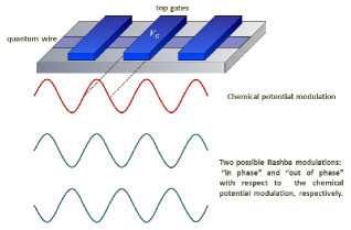
We shall assume that the wire is patterned in a heterostructure on top of which are placed a periodic sequence of equally sized nanoscale gates, positively charged and pairwise separated by the same distance as their extensions along the direction of the wire. The gates may be realized by a series of ultrasmall capacitively coupled metallic electrodes deposited on the top of the heterostructure, as illustrated in Fig. 1. By charging the gates, one produces a periodic modulation of the Rashba coupling, together with a concurrent modulation of the local chemical potential in the wire, with amplitudes depending on the associated voltage drop across the well (proportional to the gate voltage ). The modulation will be smoothly varying along the wire, reflecting the finite extent of the gates in addition to effects from distortions and stray electric fields. To a good approximation, the modulation can be represented by a simple harmonic and thus we may write
| (7) | |||||
Here is the amplitude of the Rashba field (local chemical potential) modulation, both of wave number . Note that the Rashba coupling and the chemical potential modulations are “in phase” when (and hence has the same sign as , which is always positive), while for the two modulations are “out of phase” by . The two possible phase relations between the Rashba and the chemical potential modulations are illustrated in Fig. 1. Assuming that the gate electrodes which produce the chemical potential modulation are positively charged, the segment of the wire below a gate has an enhanced magnitude of the local chemical potential (see Fig. 1), but with a negative sign. Note that the negative sign has been taken out of the sum in Eq. (7) (as well as in Eq. (1) which contains the uniform chemical potential)ChemPotFootnote .
The second-quantized expression for the lattice Hamiltonian in Eq. (7) provides a microscopic definition of the Rashba and chemical potential modulations and is manifestly Hermitian by virtue of the subtraction of the H.c.-term. This procedure replaces the symmetrization for a spatially varying Rashba interaction often employed in the literature as a means to ensure Hermiticity in a first-quantized continuum formalism ShermanSinova .
It is important to stress that the relation between a spatially modulated gate bias and a Rashba interaction may be more complex than transpires from our simple model. Already when tuning a gate voltage that is uniform along a quantum wire patterned in a heterostructure, the Rashba interaction has been shown to sometimes respond in a surprising way, even reversing its sign without a reversal of the gate bias Litvinov ; MatsudaYoh . In fact, the details of how the various effects mentioned above (including the external gate voltage), influence the magnitude and the sign of the Rashba parameter in a gated heterostructure have proven notoriously difficult to sort out, and remains a somewhat contagious issue Sandoval . We shall not attempt to add to this discussion, but instead focus on the physics implied by the idealized situation described by in Eq. (7).
Having defined our model by the Hamiltonian
| (8) |
with and given by Eqs. (1), (2), (6), and (7), respectively, it is now convenient to pass to a basis which diagonalizes the uniform spin-orbit interaction . For this purpose we first perform a rotation of the coordinate system by an angle around the -axis to select the direction of the combined uniform Rashba and Dresselhaus field, , as our new -axis:
| (9) |
where . We then introduce a spinor basis which diagonalizes ,
| (10) |
where the spinor components of the operator label the new quantized spin projections along , with defining the orientation of the axis around which the expectation value of the spin will now be precessing. With this, we write the transformed Hamiltonian as
| (11) |
with
| (12) | |||||
| (13) |
| (14) |
| (15) | |||||
with and .
Let us add a comment that our procedure leading up to Eqs. (11) - (15) is not to be confounded with the gauge transformation approach to two-dimensional spin-orbit interactions recently suggested by Tokatly and Sherman TokatlySherman (see also Ref. [LevitovRashba, ]). Whereas our transformation is simply a global spinor rotation, the gauge transformation in Ref. [TokatlySherman, ] is by construction a local rotation, yielding a manifest spin-charge duality. It would be interesting to explore whether the approach by Tokatly and ShermanTokatlySherman can be adapted to the case also of a modulated spin-orbit interaction, but for now we leave this for the future.
While the theory defined by Eqs. (11) - (15) may look forbiddingly complex, we shall find that a bosonization approach yields a well-controlled analytical solution in the physically relevant limit of low energies. In the next section we study the case with no electron-electron interaction, i.e. with for all in Eq. (13). This simplification allows us to focus on the key elements of our solution approach, paving the ground for the more elaborate analysis of the full theory in Sec. IV.
III Non-interacting electrons
III.1 Effective Hamiltonian
Neglecting the electron-electron interaction , and taking (assuming that there is no modulated electric field present), the remaining piece of the Hamiltonian in Eq. (11), , is easily diagonalized by a Fourier transform,
| (16) |
Here
| (17) |
with and , and where is the lattice constant. At band-filling , with the number of electrons [lattice sites], the system is characterized by the four Fermi points , where , reflecting the band splitting caused by the uniform spin-orbit interaction in Eq. (14).
To analyze the effect of adding the modulated term in Eq. (15) to , it is convenient to linearize the spectrum around these Fermi points and then pass to a continuum limit with . By decomposing the lattice operators into right- and left-moving fields and ,
we find that in this limit , with
| (18) | |||||
Here , , and , with . The normal ordering is carried out with respect to the filled Dirac sea. Note that in deriving Eq. (18) we have omitted all rapidly oscillating terms that vanish upon integration.
The Hamiltonian in Eq. (18) supports four distinct limiting cases, depending on the difference between the modulation wave number and the parameters :
In the first case , all terms in Eq. (18) proportional to or or are rapidly oscillating and thus average to zero when integrated. It follows that in this limit the model describes a two-component free Fermi gas, i.e. a metallic phase with gapless excitations. In contrast, in case , when , the corresponding terms proportional to become slowly varying and contribute to the dynamics. These terms emulate the presence of a transverse effective field, causing electrons to flip their spins along the direction of the combined uniform Rashba and Dresselhaus fields. Turning to case , with but with , one now finds that the terms proportional to are washed away upon integration, while the terms proportional to or to survive. This implies that backscattering and CDW correlations come into play, dramatically changing the physics: A band gap opens at all four Fermi points, causing a transition to a nonmagnetic insulating state. Finally, in case, , all terms in Eq. (16) contribute to the integrated Hamiltonian, leading to a rather complex theory. This case, however, where and both approach , requires a fine tuning of both the electron density (upon which depends) and the uniform Rashba interaction in Eq. (5) (upon which depends). This case is expected to be hard to realize in an experiment, and in the following we shall focus on the more accessible case .
III.2 Bosonization picture: Band insulator from modulated Rashba interaction
To see how the spectacular effect driven by the modulated Rashba interaction comes about (case in the previous section), it is useful to bosonize the theory. Using standard bosonization, we write the right- and left-moving fermionic fields as
| (19) | |||||
| (20) |
where and are dual bosonic fields satisfying , and where and are Klein factors which keep track of the fermion statistics for electrons in different branches Giamarchi_book_04 .
Inserting the bosonized forms of and into Eq. (18) and carrying out some simple algebra, one obtains the bosonized Hamiltonian
| (21) |
For the case that we are interested in, i.e. with , the component of the modulated term in Eq. (22) comes into play FootnoteOnComponent . For this case we can gauge out the small term from the argument of the cosine by the transformation and rewrite the Hamiltonian as , with Hamiltonian densities
| (25) | |||||
where
| (26) |
serves as an effective chemical potential. By tuning the density of electrons so that , the system is seen to be governed by two commuting sine-Gordon models Coleman with interaction terms and respectively, where . As follows from the exact solution of the sine-Gordon model DHN , in this case the excitation spectrum is gapped and consists of solitons and antisolitons with masses (together with soliton-antisoliton bound states, so called breathers, with masses ). A soliton (or antisoliton) corresponds to a configuration of the field , for a given component , that connects two neighboring minima of the functional potential . The previous field configurations define the set of possible ground states of with vacuum expectation values . For example, a field configuration where and supports a soliton [antisoliton] with fermion number , defined by
| (27) |
The charge and spin quantum numbers of the single-particle excitation are given by
| (28) |
The simplest single-particle excitation is obtained by considering a soliton or antisoliton in the spin component, keeping the ground state unperturbed for the spin component: , . Such an excitation has charge and spin (with spin projections along the direction of the momentum-dependent combined uniform Rashba and Dresselhaus fields). Thus, the elementary excitations of the system are free massive fermions with mass , each carrying unit charge and spin 1/2. It follows that the joint action of the modulated Rashba coupling and the chemical potential, with the electron density tuned so as to satisfy the commensurability condition , turns the electron gas into an effective band insulator. The corresponding band gap is equal to the doubled mass of the single-particle excitation, , since conservation of charge and spin requires the simultaneous excitation of a soliton and an anti-soliton. Note from Eq. (23) and the definition of after Eq. (18) that the effect of the Dresselhaus interaction is to reduce the gap. Fortunately, as we shall show in Sec. V, this unwanted effect (from the point of view of spintronics applications) is negligible when compared to the stronger Rashba interaction.
III.3 Bosonization picture in the spin-charge basis
The nature of the metal-insulator transition becomes more transparent if we treat the model in a basis with charge and spin bosons the standard basis in which to include effects of electron-electron interactions Giamarchi_book_04 . Thus introducing the dual charge fields
| (29) |
and spin fields
| (30) |
some simple algebra on Eq. (25) yields that , with
| (31) | |||||
| (32) | |||||
| (33) |
At Eqs. (31)-(33) describe two bosonic charge and spin fields coupled by the strongly (renormalization-group) relevant operator (of scaling dimension 1). This operator drives the system to a strong-coupling regime where the charge and spin fields are pinned at their ground state expectation values. Therefore, at , both charge and spin excitations develop a gap (let us call them and , respectively) and the system becomes a nonmagnetic insulator, consistent with the finding in the previous section where the system develops a gap also in the bosonic basis. As is tuned away from zero the influence of the operator in Eq. (33) gets weaker and eventually averages to zero upon integration when exceeds the insulator band gap given by the mass of charge excitations. At this point, the system then turns metallic. Therefore, the competition between the chemical potential term and the commensurability energy drives a continuous insulator-to-metal transition from a gapped phase at to a gapless phase at C_IC_transition . The (de-)tuning of in our Eq. (26) can be achieved by changing either or , i.e. the band filling () or the wave length of the gate modulation (). Either alternative poses its own experimental difficulties, although we expect that the band filling is more easily controllable, using a back gate with a variable voltage. Therefore, we shall hereafter assume that the tuning mechanism is provided by an adjustable band filling. Thus rephrasing this in a language closer to experiment by detuning the voltage of the backgate of the device so that the electron density of the quantum well is shifted from the value , one will observe a transition from a nonmagnetic insulating state into a metallic phasedensityfootnote . In this phase the electrons in the wire exhibit ordinary Fermi liquid behavior with gapless quasiparticle excitations. This kind of transition belongs to the universality class of commensurate-to-incommensurate transitions Giamarchi_book_04 : The conductivity close to the transition scales as , with the compressibility diverging as , before dropping to zero on the insulating side.
The insulator-to-metal transition just discussed corresponds to the picture put forward by Schulz in Ref. Schulz, where a Hamiltonian similar to that defined by our Eqs. (31) - (33) is refermionized into a two-band model (cf. Eq. (4) in Ref. Schulz, ). The two bands are separated by a gap , with a chemical potential corresponding to a completely filled lower band. In other words, in this state the system is a band insulator with a gap . For smaller than the critical value , holes are introduced at the top of the lower band, whereas for larger than , electrons are added to the bottom of the upper band; in both cases the system becomes metallic. This refermionized picture thus makes it clear that it takes a finite critical for the transition to occur: by tuning the chemical potential to zero the system not only develops a gap but also a rigidity that sustains the gap when the system is shifted away from commensurability.
Going back to Eqs. (31) - (33), it is instructive to see how the single-fermion excitations obtained in the previous section can be reconstructed in the present spin-charge basis. Here we follow a route developed in Ref. FGN, in studies of a similar problem in the case of the ionic Hubbard model. First note that only the relative sign between and in Eq. (33) is fixed to be negative (so as to minimize ). Thus, there are two possibilities for the ground state charge and spin field expectation values:
| (34) | |||||
| (35) |
with . To obtain the single-fermion excitations one has to consider field configurations that connect two groundstates that belong to distinct sets I (Eq. (34)) and II (Eq. (35)). As an example, a field configuration that connects with in the charge sector and with in the spin sector corresponds to an excitation with charge and spin quantum numbers GNT
| (36) | |||||
| (37) |
i.e. a massive fermion (of mass ), which is the elementary excitation in the band insulator. To obtain a pure charge or spin excitation one must consider field configurations that connect groundstates within the sets I and II. For example, given set I in Eq. (34), we can lock the charge at and consider a spin soliton connecting the groundstates at and . Such an excitation carries charge and spin
| (38) |
In the noninteracting case considered here it is clear that that this excitation is built from two massive fermions with opposite charge and the same spin. Similarly, a charge soliton can be obtained by locking the spin at one of the possible groundstates and consider a charge field configuration that connects, say, and . This excitation carries charge
| (39) |
while having zero spin, being built from two massive fermions with the same charge and opposite spin.
Following this logic, a derivation of and should give . As we shall see, the mean-field approach used in the next section to evaluate and gives a slightly overestimated value. We shall return to this issue below, and show how it can be resolved by a proper regularization procedure.
The opening of a gap for both charge and spin excitations SSH at commensurability, , reflects the fact that the system has turned into a nonmagnetic band insulator. Using the standard bosonized expression for the charge density, GNT
| (40) |
with a constant, one verifies from Eqs. (34) and (35) (which apply at ), that the ground state of the system corresponds to a CDW-type band insulator, with long-range charge-density modulation
| (41) |
where
| (42) |
As should be clear from the non-conservation of spin in the presence of the spin-orbit interactions, the massiveness of the spin excitations does not correspond to the formation of a spin density wave (SDW). Indeed, by writing down the bosonized expressionGNT for a SDW with spin projection along the direction of the combined uniform Rashba and Dresselhaus fields, , with a constant, one immediately verifies from Eqs. (34) and (35) that it has no amplitude for a long-range modulation.
III.4 Bosonic mean-field theory in
the spin-charge basis
To pave the ground for including electron-electron interactions into the problem, we next decouple the interaction term in Eq. (33) in a mean-field manner by introducing
| (43) | |||||
| (44) |
Note that the mean-field decoupling is well controlled since, at the strong-coupling fixed point, fluctuations are strongly suppressed by the pinning of the charge and spin bosons. Using Eqs. (43) and (44), we find that the mean-field version of the bosonized Hamiltonian , defined in Eqs. (31) - (33), can be written as with
| (45) | |||||
| (46) |
When , the Hamiltonian defined by Eqs. (45) and (46) is again given by a sum of two decoupled sine-Gordon models (cf. Eq. (25)). However, the dimensionalities of the operators at [spin-charge basis, Eqs. (45), (46)] and [ basis, Eq. (25)] are different.
By exploiting the exact solution of the sine-Gordon model, we can easily estimate the size of the insulating gap in the spin-charge basis JHLM-H_2007 . The excitation spectra of Eq. (45) at and Eq. (46) consist of solitons and antisolitons with masses and , respectively (in addition to the charge and spin breathers with masses bounded below by and , respectively). These charge and spin soliton masses are related to the “bare” masses and in Eqs. (45) - (46) by Al_B_Zamolodchikov_95
| (47) |
with an energy cutoff that blocks excitations into the second conduction channel of the quantum wire (for details, see Sec. V).
The ground state expectation values of are in turn given by Luk_Zam_97
| (48) |
with and (For details, see Appendix A.) By combining Eqs. (47) and (48) with (43) and (44) one reads off that
| (49) |
with .
Note that charge and spin solitons, though formally decoupled, move with the same velocity (cf. Eqs. (45) - (46)), a record of their composite nature since, as demonstrated in Sec. III.C, charge and spin excitations are built from single fermions of mass , unit charge and spin , the latter being the elementary excitations in the basis of Sec. III.B. Thus, the mean-field treatment in the spin-charge basis faithfully captures the character of the excitations. However, the size of the two-particle gap, or as given in Eq. (49), gets overestimated by a factor of 1.7 when compared to the result , obtained in Sec. III.B. As we shall show in the next section, the factor of 1.7 can be removed by introducing a regularized form of the gap.
Recall that tuning the effective chemical potential away from zero “closes” the band gap, and thus drives an insulator-to-metal transition by depinning the charge field from its ground state expectation value. The combined Eqs. (44), (47), and (48) reveal that, in the process, the spin sector becomes gapless as well, as .
III.5 Functional behavior of the effective band gap
Having established that the masses of the charge- and spin excitations in the non-interacting theory, and respectively, are determined by the single-fermion mass , let us return to Eq. (23) to analyze its dependence on the relative phase between the two modulations and their amplitudes and . As emphasized in the previous sections, the mass is a key parameter of our theory, encoding the effective band gap in the insulating state of noninteracting electrons.
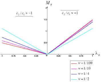
In Sec. V, when analyzing a generic gated heterostructure, we shall see that both and depend linearly on the voltage of the top gates (cf. Fig. 1). We may thus write and , where and are constants depending on the details of the setup and of the sample.
To analyze the gap behavior it is important to distinguish the two ways in which the parameters and can be varied: One possibility is to consider (i) a fixed system (i.e. keeping and fixed) and varying the gate voltage ; alternatively, one may consider (ii) different systems but keeping the gate voltage fixed, e.g. by testing different samples from an ensemble of properly gated heterostructures (all of which satisfy the commensurability condition ).
Let us start by investigating the possibility (i). In this case, we can rewrite and Eq. (23) as
| (50) |
where is a system specific parameter adjustable by the band filling (which, in turn, can be varied by a back gate with a variable voltage).
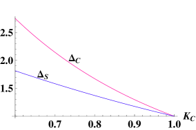
Figure 2 shows as a function of for band fillings . The reason for considering systems only up to half-filling is the following: Due to the commensurability condition , the values of the filling in Figure 2 correspond to modulation wave lengths and , respectively (as seen from the relations and ). Since the ultrasmall gates that we propose to be used for producing the modulation each has a spatial extension along the quantum wire (c.f. Figure 1), it follows that sets an upper (and in practice, unattainable) physical limit for possible band fillings: If , the dimension of a gate would have to become subatomic. In fact, as can be gleaned from the experimental data cited in Sec. V, our theory would likely break down already for band fillings around since at larger fillings higher subbands will come into play, causing subband mixing. As we shall also see in Sec. V, the 1D band filling with present-day semiconductor heterostructures is typically around , implying a gate extension of a few nanometers. Already this presents a challenge to the experimentalist.
The plots in Figure 2 are shown for running from to , thus accounting for the two possible phase relations between the Rashba and the chemical potential modulations. For “in phase” [“out of phase”] modulations, the plots are shown for test systems where [].
.
We see that for both “in phase” and “out of phase” modulations, the gap is an increasing linear function of with slope depending on the band filling. The increase of the gap is consistent with the phenomenological expectation that the insulating state gets more stable as the pinning Rashba interaction goes stronger, and is in agreement also with the corresponding result in Ref. JJF_Paper_09, . There, however, the modulation of the charge density was not taken into account and, thus, the formalism did not capture the gap dependence on the band filling. The split of a single gap line for different values of , as manifest in Figure 2, is an interesting feature of the system resulting from the combination of the modulated Rashba interaction and CDW correlations.
Another interesting aspect of the gap behavior is that, given a certain band filling and a value for , the gap for “in phase” modulations is larger than for “out of phase” modulations, implying a stronger localization effect when the the Rashba interaction and the chemical potential act in “unison”. The difference goes to zero as approaches 1/2 (half-filled band).
Turning now to case (ii), we can define a new variable that characterizes a particular setup, material, or design and is independent of the value of the applied gate voltage. With that we can rewrite Eq. (23) as
| (51) |
where .
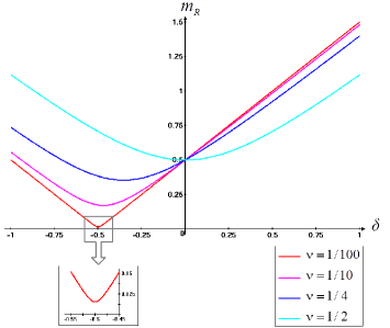
Figure 3 shows as a function of for the same band fillings used in case (i). The plots are shown for running from to , accounting for “in phase” and “out of phase” Rashba and chemical potential modulations.
To understand the behavior revealed by Figure 3, let us first look at the right-half of the graph where the Rashba and chemical potential modulations are “in phase”. The plots here show a monotonic increase of with , implying that with devices where the top gate voltages have been tuned so as to produce the same fixed value of , the gap will be larger in the device with the larger value of . This behavior is equivalent to that obtained in case (i).
Now turn to the left-half of the graph where the Rashba and chemical potential modulations are “out of phase”. Again comparing devices having the same band filling and for which the magnitude of the gate voltages have been tuned to give the same , we observe an unexpected feature. Let us follow what happens when going through different devices by moving along a curve with a fixed band filling (smaller than 1/2): the gap first decreases with the strength of the Rashba interaction until it reaches a minimum at ; past this value the “normal” increasing behavior is recovered. This crossover behavior gets more pronounced for smaller values of , i.e. as the system goes more diluted. For , for example, the crossover almost annihilates the gap at (but not completely as can be seen by zooming in around that point).
To understand how this phenomenon comes about, consider a Gedanken experiment with a single device where is allowed to vary while is kept fixed. In the case with anti-phased modulations, the chemical potential [Rashba potential] will have a maximum [minimum] in the middle of the segment, call it “A”, below one of the small positively charged gates (and vice versa for a neighboring gate-free segment, call it “” (cf. Fig. 1)). Consider first the case with . Here all electrons will reside in the -regions since this configuration is energetically more advantageous. This causes a localization of electrons, with a gap as seen in Figure 3 for . Now turn on . To take advantage of the spin-flip Rashba hopping some electrons will start migrating into the -regions. This weakens the localization effect of the chemical potential modulation, with the result that the gap decreases. By successively increasing , more and more electrons will migrate into the -regions, and for a sufficiently large value of , equal to , all electrons will reside in the -regions. From that point on the gap will increase monotonically as (or ) is further increased, as displayed in Figure 3. For fillings close to the upper physical limit, that is 1/2, a small is enough for a complete electronic migration between the chemical potential -regions to the spin-orbit coupling -regions while, for a more dilute system, the process is “slower”, demanding a larger . The two extreme cases are for which the -regions are emptied right away for any nonzero and for which the necessary is (still just) half the amplitude of the original pinning chemical potential.
In the next section we shall investigate how the electron-electron interaction influences the results thus obtained.
IV Interacting electrons
IV.1 Adding interactions: Bosonization picture
in the spin-charge basis
To incorporate the electron-electron interaction in Eq. (13) into the bosonic theory we perform the same steps as in Sec. III.B, first linearizing the spectrum around the four Fermi points and taking a continuum limit. This yields , with
| (52) | |||||
with summed over, and where and are the amplitudes, respectively, for back and forward (“dispersive”) scattering between electrons of different chiralities, and is the amplitude for forward scattering between electrons of equal chirality Giamarchi_book_04 . Whereas the and processes correspond to scattering with small momentum transfer, the process transfers momentum . For a screened Coulomb interaction with a nonzero screening length, the amplitude is therefore quite small, and can usually be neglected. This is certainly so in the present case since in a semiconductor structure the Coulomb interaction is much smaller than the band width. It follows that in this limit the scattering becomes marginally irrelevant and renormalizes to zero at low energies. Importantly, this conclusion is not invalidated by the presence of the spin-orbit couplings GJPB_05 . From now on we shall therefore consider the simpler theory where the back scattering has been renormalized away, i.e. with .
For a system at commensurate band-filling , with an integer, the Hamiltonian density in Eq. (52) should be supplemented by an umklapp term which describes the transfer of electrons of equal chirality to the opposite Fermi point through exchange of momentum with the lattice. As is well known, these processes drive a transition to an insulating state at a critical value of the Coulomb interaction determined by the number of electrons participating in the process GiamarchiMillis . However, the screened Coulomb interaction in a gated semiconductor structure is too weak to support such a transition except at a half-filled or possibly a quarter-filled band Hausler . This should be contrasted with the commensurability condition for driving a metal-to-insulator transition via a modulated Rashba interaction, as derived in Sec. III.B. Since , with the wavelength of the Rashba modulation, and , this condition translates to when . Thus, with a Rashba modulation tuned to commensurability with , umklapp processes at could come into play only for a sequence of electrical gates of near-atomic dimensions, . For this reason we shall neglect umklapp processes when studying the novel physics coming from a Rashba modulation.
Having disposed of backscattering and umklapp processes, the remaining electron-electron interaction in Eq. (52) is now easily bosonized using Eqs. (19), (20), (29), and (30). The resulting expression for the bosonized mean field theory representing the full in Eq. (11) then takes the form , with
| (53) | |||||
| (54) | |||||
where we have performed the field transformations and . A comparison with Eqs. (45) and (46) shows that has the same structure as the mean field theory for noninteracting electrons and is given by two decoupled sine-Gordon models when the commensurability condition is satisfied. The electron-electron interaction is encoded by the new parameters and , as well as by the reparameterization of the bare masses and due to the transformation (cf. Eqs. (43), (44)). In the weak-interaction limit considered here, and can be given explicit representations in terms of the scattering amplitudes in Eq. (52). Introducing the conventional “g-ology” notation Giamarchi_book_04 for parallel spins and for opposite spins, one has that
| (55) |
| (56) |
for , where
| (57) |
| (58) |
with the upper and lower signs in eqs. (58) referring to and , respectively. If backscattering processes were to be included in the theory, in Eq. (58). In addition, the parameter in the spin sector would become subject to a RG flow, coupled to the marginally irrelevant flow of , the amplitude for backscattering of electrons with opposite spins Giamarchi_book_04 . The breaking of spin-rotational invariance by the presence of spin-orbit interactions implies that the RG fixed-point value of , call it , is not slaved to unity but can take larger values. However, with the backscattering processes being weak the resulting renormalization would be small. We will return to this issue in Sec. V.
IV.2 Charge-, spin-, and single-particle gaps
Given the bosonized mean-field theory defined by Eqs. (53) and (54) we shall now address the question of how electron-electron interactions influence the Rashba-induced single-particle gap established in Sec. III.B. As anticipated in Sec. III.C, this task gets complicated by the fact that already for noninteracting electrons the excitation gap in the spin-charge basis is nontrivially related to the single-particle gap, being in effect a composite two-particle gap. Moreover, as seen in Eq. (49), the mean-field theory in the spin-charge basis overestimates the actual size of this two-particle gap. The situation for interacting electrons gets further confounded by the fact that the spin and charge gaps are no longer identical, but take on separate values, reflecting the collective nature of the excitations in the presence of electron-electron interactions.
Taking off from Sec. III.D where we calculated the mean-field charge soliton mass and spin soliton mass for the case of non-interacting electrons, we perform a similar procedure, now with electron-electron interactions included, starting with the reparametrized sine-Gordon models in Eqs. (53) and (54). Note that by construction, and in exact analogy with the noninteracting case discussed in Sec. III.D, and are the mean-field approximations of the spin and charge gaps of the fully interacting theory, and respectively. Using Eqs. (43), (44), (53), and (54), we get the following relations between and :
| (59) |
where satisfies
| (60) |
with given by the same expression, but with , and where , , are defined in Appendix A.
The mean-field version of the noninteracting theory is recovered by choosing , for which
| (61) | |||||
with the identical number for , the result which we arrived at already in Eq. (49) via a slightly different route. Thus, to repeat, while the mean-field theory correctly reproduces the identity for noninteracting electrons, the size of the corresponding two-particle gap gets overestimated by a factor of 1.7.
We can improve upon the situation by dividing away this number for all and , thus in effect defining a regularized version of the mean-field spin and charge gaps,
| (62) |
with , given in Eq. (59). By construction, this produces gives the correct noninteracting limit.
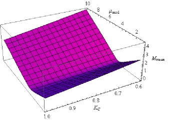
Fig. 4 shows and for the experimentally relevant parameter range and . (As an example, to be elaborated upon in Sec. V, a generic quantum wire obtained by gating an InAs heterostructure is well described by taking and .) The fundamental features of the influence of electronic interactions on the charge and spin gaps can be gleaned from Fig. 5 that shows a projection of the previous surfaces on the plane.
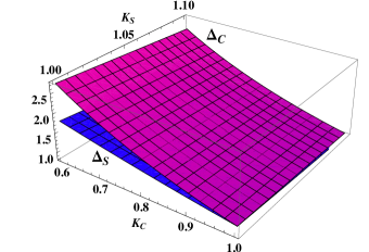
As is manifest by these curves, the important property that , expected on physical grounds Giamarchi_book_04 , is respected by the regularized mean-field gaps. The equality is valid at , that is, in the absence of electronic interactions, reproducing the result of Sec. III.D.
Fig. 5 also shows that both charge and spin gaps are decreasing functions of the parameter . Since decreases with increasing -couplings (c.f. eqs. (56)-(58)), our results show that the gaps increase with the -couplings, i.e. are robust against electronic interactions. Note that the impact of electronic interactions is particularly strong on the charge gap, which, in the considered range of parameters, more than doubles by increasing the strength of electronic interactions.
Let us proceed to the calculation of the single-particle gap which, in the experimentally relevant case of electron [hole] transport through a quantum wire, defines the characteristic energy scale of the system. In particular, this is the gap that determines the current blockade effect, the key element in a spin transistor design based on a modulated Rashba interaction.
Let us first recapitulate the formal definitions for single-particle gaps following the classification used in Ref. Manmana, . The single-particle gaps are defined as the energies necessary to add to the system one electron or one hole with spin projection :
| (63) | |||||
| (64) |
In the case of non-interacting electrons, studied in Sec. III.B, we identified the single-particle gaps with the mass of the fermionic quasiparticles (massive sine-Gordon solitons and antisolitons in the basis): . footnoteSpin We are now equipped to take on the calculation of the single-particle gap in the presence of electronic interactions. As we will not be able to resolve the particle- and hole gaps in Eqs. (63) and (64), we instead focus on the average single-particle gap
| (65) |
with corresponding to the energy required to add two particles with opposite spin, and the energy to add a particle and a hole with the same spin. Now, as we saw in Sec. III.C, a charge soliton (of mass ) is precisely built from a pair of fermions carrying opposite spin, with a spin soliton (of mass ) being composed of a particle-hole pair in a spin triplet state. While these properties were established for the case of noninteracting electrons, the generalizations of Eqs. (38) and (39) to the case of rescaled fields,
| (66) | |||||
| (67) |
show that the relation between the gaps as determined by the assignment of quantum numbers are unchanged by electron interactions. It follows from Eq. (65) that
| (68) |
from which we infer with the help of Eqs. (59) and (62) the mean-field (average) single-particle gap
| (69) |
with
| (70) |
and where is given by Eq. (23). Eq. (69) is the key result on which we shall build our analysis in the next section. In the limiting case of non-interacting electrons, where , , and , we obtain, from Eq. (69), and thus recover the result of Sec. III.B.
In Fig. 6 we have plotted in the range , for and with meV, , meV, and 1 meV meV. (The previous values correspond to the case study carried out in Sec. V.) Again, note the significant effect of the electron-electron interactions on the size of the single-particle gap: decreasing the strength of electronic interactions, the gap also decreases.
V Application: Towards a new type of current switch?
In Ref. JJF_Paper_09, it was argued that the insulating gap that opens when the Rashba modulation becomes commensurate with the band filling is sufficiently large to be exploited in a spin transistor design. When the modulation is turned off, the electrons are free to move and will carry a current when a drain-to-source voltage is applied. By charging the gates thus turning on the modulation the system becomes insulating and the current gets blocked. A rough estimate in Ref. JJF_Paper_09, , using data for a gated InAs heterostrucuture Grundler , suggested a drain-to-source threshold voltage of the order of 100 mV. In this section we revisit the problem, now equipped with a more complete theory which sports a refined formula for the single-particle gap, Eq. (69), as well as a description of effects from the concurrent modulation of the chemical potential.
For a new type of current switch to become competitive it is essential that the ON-OFF switching time compares favorable with that of the ubiquitous MOSFETs that are used in present day electronics. Since grows with the applied gate voltage (with the power dissipation during switching being proportional to the square of the gate voltage), we shall consider the case where the device operates at or below a typical gate voltage of a MOSFET, in the 1 V range or lower. While the gate-controlled built-in electric fields in a doped heterostructure can be quite strong, the issue is whether the resulting Rashba effect now combined with the chemical potential modulation can become sufficiently large to be used as a switch with a gate voltage of this moderate size. An important constraint is here that leakage currents must be prevented in the OFF state. The present dominance of silicon CMOS devices for current switching is largely due to the fact that there is virtually no leakage current in the OFF state of a MOSFET, effectively protecting against unwanted signals as well as against standby power dissipation. Since an assessment of possible sources of leakage currents can only be made on basis of a specific technical design, we will not be able to fully address this constraint here. However, the minimal requirement that thermal leakage of charge must be prevented will be an important bench mark in our analysis. At room temperature, it translates into the requirement that the gap should be meV. Clearly, this is a lower bound. Heating of the device, as well as the requirement that the source-to-drain voltage must not be too small, points to a minimum gap around, maybe, 100 meV. This is the number quoted in Ref. JJF_Paper_09, , but can it be reproduced within our more elaborate theory?
To find out, we must assign numbers to the parameters , , and that enter the expression for the single-particle gap in Eq. (69). We shall use the same data source as in Ref. JJF_Paper_09, , obtained from the experimental work by Grundler on gate-controlled Rashba interaction in a square asymmetric InAs quantum well Grundler . By adjusting the gate voltage appropriately after application of a LED pulse (which increases the 2D carrier density via the persistent photo effect), Grundler succeeded to tune the Rashba spin splitting without charging the 2D channel, thus allowing for a direct probe of the gate-voltage dependence of the Rashba parameter . For our purpose, this is an important feature, since in our model we treat as being independent of the electron density. Let us add that quantum wells based on InAs, realized in In1-xGaxAs/In1-xAlxAsGrundler ; Nitta97 ; Hu ; Koga or InAs/AlSbHeida heterostructures, are preferred choices in many proposals for spintronics applications due to their typical large Rashba couplings eVmNitta97 . Moreover, unless the quantum well is designed with a very small valence band offset, it is also safe to assume that , with the Dresselhaus couplingMeier . As we have found that the Dresselhaus interaction reduces the size of the insulating gap, this is an additional desired feature of the InAs quantum well probed in the experiment by Grundler Grundler . In what follows we assume that the heterostructure studied in Ref. Grundler, has been gated so as to define a single-channel micron-range ballistic quantum wire.
V.1 Band gap for non-interacting electrons
Let us start by estimating the insulating band gap for the non-interacting theory. As already discussed, the band gap is twice the single-fermion mass , defined in Eq. (23).
Taking , we neglect the presence of the Dresselhaus interaction completely, for which case . By inspection of Eq. (23), an estimate of then requires numbers for , , and .
Beginning with , we assume that this amplitude depends on the voltage of the small periodically spaced gates that produce the modulation (see Fig. 1) in the same way as depends on a uniform gate voltage. This is a reasonable assumption since neglecting random fluctuations from dopant ions SJJ the internal electric field in the quantum well that supports the Rashba interaction is primarily determined by the slope of the band edge along the growth direction of the heterostructure (perpendicular to the 2D InAs quantum well interface), and hence its (extremal) value right below the center of one of the small periodically spaced gates should approach that for the case of a single large gate. Inspection of Fig. 2 (b) in Ref. Grundler, reveals that the Rashba interaction in the device considered decreases by roughly eVm with an increase in gate voltage of 0.1 V, indicating that the Rashba and the chemical potential modulations are out of phase by . As an aside, note that the data in Fig. 2 (b) in Ref. Grundler, confirms the theoretical expectation that the change of the Rashba coupling with applied gate voltage is linear, a fact that we used in Sec. III.E when analyzing the functional dependence of the effective band gap. Translating to our geometry, the decrease of the Rashba interaction with a positive increase of gate voltage implies that there is a minimum negative offset, call it , from the uniform value with no gates present. This is due to the fact that the transverse component of the net gate electric field (which controls the Rashba interaction) has a nonzero value at the midpoint between two gates. In other words, the maximum value of the total Rashba interaction (uniform + modulated) in the presence of the small gates is given by and is attained at the midpoint between two gates. Using the data quoted from Ref. Grundler, , it follows for the amplitude of the Rashba modulation that eVm. The magnitude of the offset is small compared to and hence we take eVm. We then have that meV, where Å is the lattice spacing in epitaxial InAs Hornstra . With , this in turn implies that meV.
Turning to the amplitude of the modulated chemical potential, it is here more difficult to obtain an accurate number and we will have to do with a rough estimate. There are two types of contributions to from the external gates; one coming from the transverse component of the applied gate electric field (enabling a local migration of charge from the quantum well into the dopant layers), the other from its longitudinal component, inducing a rearrangement of charge inside the quantum wire. We expect the latter to dominate the modulation of the local chemical potential and here neglect the small residual charge migration caused by the transverse electric field. As for the variation of the longitudinal electric field along the wire, an exact expression requires a precise description of the fringe fields and their superpositions from the periodic sequence of top gates. This goes far beyond the scope of our minimal approach here, where we assume the simplest possible, but still physically meaningful, behavior: a longitudinal electric field that oscillates harmonically along the wire: , choosing just below the center of one of the top gates. The variation of the chemical potential along the wire is then related to the negative work required to bring an electron to ,
| (71) |
where . Note that the chemical potential variation of Eq. (71) is indeed the one assumed in the very construction of our model, Eq. (7).
With the assumption that the amplitudes of the longitudinal and transverse components of the net gate electric field are of the same order of magnitude, we make the approximation , where is the voltage of a gate electrode and is the perpendicular distance between the gate and the wire. Thus, . From the commensurability relation , with the 2D electron density of the InAs quantum well, we arrive at the desired expression for is terms of experimental parameters:
| (72) |
From Ref. Grundler, we have that nm and m Using a gate voltage V, we obtain that meV. This number will get modified when including effects from Fermi statistics, Coulomb interaction, and the presence of the transverse component of the applied gate electric field. However, guided by experimentally inferred Fermi level variations with gate voltage in other InAs quantum wells Nitta97 ; Hu ; Koga , we expect that our estimate of for the geometry considered and with the type of heterostructure used in Ref. Grundler, lies within reasonable bounds. To have some margin for error, we must actually quote only as taking possible values in a range including 4 meV. Going back to Fig. 4, we see that the single particle gap in the presence of electron-electron interactions is not a monotonic function of , displaying a minimum exactly around 4 meV. So, restricting the error bar to lie inside the regime of interest (from the point of view of spintronics applications) of increasing gap, we consider assuming values in the range from 4 meV to 10 meV.
In order to obtain a value for in Eq. (23) (or rather, an interval for possible values for , considering the numerical uncertainty in the -parameter), it remains to determine the 1D band filling . With the assumption that the quantum wire has only a single conducting channel this is straightforward. The data for the Rashba variation with top gate voltage in Ref. Grundler, were taken at a constant electron density m-2. With the Fermi wave number for the quantum wire expected to be roughly the same as for the 2D electron gas, this translates, via , into:
| (73) |
Putting in the numbers, we get .
Inserting our estimates
into Eq. (23), we finally obtain that
| (74) |
with the upper bound corresponding to meV, and with the lower bound attained for meV. Note the minus sign in , indicating that the two modulations in the type of device considered are antiphased, which is the reason for the non-monotonic behavior of the gap as a function of (cf. discussion in Sec. III.E).
We should here point out that given the value of in Ref. Grundler, , our use of a single 1D conducting channel is not an unreasonable assumption. A first estimate, using an infinite-well confinement potential may suggest that a quantum wire with diameter nm would satisfy the single-channel condition: nm. However, with the Fermi energy meV (with for a gated InAs quantum wire Grundler , where is the electron mass), self-consistency requires that the wire is not much wider than roughly since otherwise the Fermi level would cut through the first subband. In addition, for our modeling to make sense, our energy cutoff , first introduced in Eq. (47), must be smaller than the distance from the Fermi level to the bottom of the first subband. Below we shall choose meV, which again assuming an infinite-well confinement with requires the wire to be at most 7 - 8 nm wide, still, however, within the realm of present-day technologyFerry . One should note that a more realistic soft confinement potential could possibly open an additional conducting channel and lead to population of the first 1D subband, in which case our model would no longer apply. However, as the gate-controlled Rashba effect in Ref. Grundler, appears to be rather insensitive to a lowering of the value of , this potential problem should in principle be easy to overcome (cf. Fig. 2 (b) in Ref. Grundler, ).
V.2 Band gap for interacting electrons
To complete our analysis of the single-fermion mass, we need to include the effect of electron-electron interactions. These are encoded by the Luttinger liquid charge- and spin parameters and . Using that the forward scattering amplitudes in Eq. (56) are all equal and given by the (zero momentum transfer) Fourier component of the screened Coulomb interaction Giamarchi_book_04 , , we obtain from Eq. (56), neglecting the small correction from backscattering processes with momentum transfer ,
| (75) |
The screening length of the interaction is roughly set by the perpendicular distance between the quantum wire and the nearest metallic gate. A detailed analysis ByzcukDietl leads to the expression
| (76) |
where is the radius of the quantum wire and is the averaged relative permittivity of the dopant and capping layers between the quantum well and the nearest gate, at a distance from the wire. As an interesting aside, note that the leading logarithmic term in Eq. (76) depends only on the permittivity of the environment and not on that of the wire, implying that electrons interact mainly with image charges and not with other electrons in the wire. With the backgate of the device in Ref. Grundler, being at a distance nm from the quantum well, and with an averaged permittivity for the interjacent In0.75Al0.25As and Si-doped In0.75Al0.25As layers Bhattacharaya , we obtain from Eqs. (75) and (76) that , taking 5 nm and using that m/s Bhattacharaya . We should alert the reader to the fact that the estimate for also comes with some uncertainty, considering that it is obtained using the parameterization in Eq. (56) which is strictly valid only in the weak-coupling limit . Still, Bethe Ansatz and numerical results for this class of models have shown that the weak-coupling formula in Eq. (56) does surprisingly well in capturing effective parameters also for intermediate strengths of the electron interaction when, as in the present case, the band filling is low, thus providing indirect support for our estimate Schulz2 .
Turning to the spin parameter , we already noted in Sec. IV (text after Eq. (58)) that its bare value predicted by Eq. (56) will renormalize to a value slightly larger than unity due to backscattering of electrons. Having ignored these scattering processes when writing down the spin Hamiltonian in Eq. (54) with the rationale that they are weak in a semiconductor device, we may compensate for their omission by adjusting the value of by hand, setting it slightly larger than unity, say at . Guided by work on other models where takes values different from unity we expect this to be a reasonable estimate GJPB_05 . In what follows thus represents the expected RG fixed point value , carrying an imprint of the marginally irrelevant backscattering term in the spin sector. It may be worth pointing out that the correction to due to backscattering is smaller than that for and is here neglected.
Having put numbers on and we now go back to Eq. (60) and calculate, with the help of Eqs. (83) and (85) in the Appendix,
| (77) | |||||
| (78) |
Combining this with Eqs. (61), (69), (70), and (74) and taking meV, we finally obtain an estimate for the single-particle gap ,
| (79) |
Summarizing its specification, this result applies to a periodically gated 5 nm thin quantum wire embedded in a Rashba-active heterostructure of the type studied in Ref. Grundler, , assuming that the Fermi wave number has been properly tuned to commensurability with the gate spacing, and taking the gate voltage to be +0.1 V. Note that the length scale at which the gap starts to open up lies within the interval 0.1 m 1 m, with the lower [upper] bound corresponding to meV [0.4 meV], thus fitting well within the ballistic regime of an InAs quantum wire Hornstra .
The estimate in Eq. (79) is strikingly lower than that in Ref. JJF_Paper_09, , where the same kind of system was analyzed using a simpler theory. One of the missing ingredients in that theory is the interplay between the modulation of the Rashba interaction with that of the local chemical potential, an effect that we have found to cause a significant reduction of the gap. Also, the gap in Ref. Grundler, was extracted from that of the collective charge excitations of the low-energy effective model, and not, as in the present approach, properly reconstructed as a single-particle gap, which is the one relevant for charge transport CorrectionFootnote .
One notes that already the gap at the upper bound in Eq. (79) is far below the thermal threshold of meV that is required to block thermal leakage of charge a sine qua non for a functioning current switch. Thus, a usable device based on spin-orbit and charge modulation effects will clearly require a different type of heterostructure and/or input parameters than what we have assumed here. A significant improvement would be achieved if by “band engineering” Litvinov ; MatsudaYoh one could grow a heterostructure where the Rashba and chemical potential modulations are in phase, not out of phase as in the case study above. As evidenced by Eq. (23) and discussed in the context of Fig. 2, this will boost the resulting gap, especially for the case of low electronic density. Secondly, our analysis shows the importance of having a large electron-electron interaction. This, in principle, is obtainable by further reducing the electron density, with the added advantage of making the required gate spacing larger (as seen in the commensurability condition with and ) thus giving leave for larger and experimentally more tractable gates. Finally, and most obvious, by allowing for a larger gate bias than the 0.1 V used in the estimates above, the gap opening effect will be further boosted. Still, unless one allows for very large voltages, in the 5-10 V range, the gap as estimated within our formalism and for the system specifications used here will be too small for making a credible case for a working current switch at room temperature. At these large voltages, however, our proposed device would have no clear advantage compared to standard silicon CMOS designs. Moreover, since the growth of the modulated Rashba coupling will have saturated at much smaller voltages, any additional gap opening effect will primarily be due to the CDW correlations from the modulated chemical potential, not to the presence of a Rashba interaction.
Before closing the case, however, we wish to stress that our numerical estimates have been obtained by filtering experimental data through an effective low-energy field theory formalism based on a highly simplified lattice model. We have tried to be careful in processing the data, however, the approach we use is not optimally adapted for this task. As we have repeatedly pointed out, this makes our numbers marred with uncertainty. Whereas our theory does provide a “proof-of-concept” of using a periodically gated quantum wire for a low-bias current switch, a definite verdict about its practicability requires more work, based on a more sophisticated approach in modeling and analysis.
VI Summary
In conclusion, we have analyzed the spin- and charge dynamics in a ballistic single-channel quantum wire in the presence of a gate-controlled harmonically modulated Rashba spin-orbit interaction, and with a concurrent harmonic modulation of the local chemical potential. To be able to model a quantum wire in a gated heterostructure with lattice inversion asymmetry, we have also allowed for a uniform Dresselhaus spin-orbit interaction.
Depending on the relation between the common wave number of the two modulations, the Fermi momentum , and a parameter which encodes the strength of the Dresselhaus and the uniform part of the Rashba interaction, the electrons in the wire may form a metallic or an insulating state. Specifically, and most interesting from the viewpoint of potential spintronics applications, when and (with the lattice spacing), a nonmagnetic insulating state is formed, with an effective band gap which depends on the amplitudes of the Rashba and chemical potential modulations as well as on the strengths of the uniform Dresselhaus and Rashba interactions. Whereas the Dresselhaus interaction reduces the band gap, the uniform part of the Rashba interaction increases its size. The gap also increases with the amplitude of the modulated part of the Rashba interaction, but only if the local chemical potential modulation is in phase with that of the Rashba interaction, or if the amplitude of the Rashba modulation is larger than some threshold value of the chemical potential modulation. Else, the gap is a decreasing function of the Rashba modulation amplitude. The resulting crossover behavior of the effective band gap is controlled by the band filling, which sets the threshold value of the chemical potential modulation.
This gap-opening scenario, including the crossover behavior, is found to be robust against electron-electron interactions. To arrive at this conclusion we used a bosonization approach, mapping the interacting problem onto two mean-field decoupled sine-Gordon models. By a careful analysis of the structure of the ensuing charge- and spin gaps, we devised a regularization scheme from which the size of the single-particle gap can be reconstructed, and which allowed us to determine its dependence on the strength of the electron-electron interaction. Exploiting exact results for the sine-Gordon model we found that the gap scales as where is the sine-Gordon soliton (or antisoliton) mass for noninteracting electrons, and where and are the Luttinger liquid charge- and spin parameters, respectively. Whereas the scaling exponent agrees with that found in Ref. JJF_Paper_09, , our estimate for the band gap (using data from the same experimental setup as that studied in Ref. JJF_Paper_09, ) comes out dramatically smaller: As discussed in the previous section, the theory in Ref. JJF_Paper_09, does not include the competition between Rashba and chemical potential modulations in the experimentally relevant parameter regime, and moreover, the band gap is not properly reconstructed as a single-particle gap from the collective spin- and charge excitations in the bosonic spin-charge basis CorrectionFootnote .
While our analysis reveals shortcomings with proposals JJF_Paper_09 ; Wang ; GongYang to use present-day materials and designs for constructing a low-bias current switch from a gate-controlled modulated Rashba interaction, it also points to possible routes to overcome the problem. Besides the obvious measure to search for materials with larger Rashba couplings, we have shown the importance to engineer heterostructures where the gate-controlled Rashba modulation is in phase with that of the local chemical potential produced by the gate configuration Litvinov ; MatsudaYoh . We have also shown that the size of the effective band gap can be significantly boosted by reducing the electron density in the quantum wire; this leads to a reduction of the screening of the electron-electron interaction, and, with that, a larger gap-opening effect from the Rashba modulation.
From a more fundamental perspective, questions about how the gap-opening scenario is influenced by disorderDisorder , magnetic field effectsMagneticField , and subband mixing NONINTERACTING are yet to be addressed. These become challenging problems in the context of a spatially varying spin-orbit interaction, and may require a theoretical approach that goes beyond the effective field-theory approach that we have used here. Even with these questions unanswered, however, our prediction of an electrically driven commensurate-to-incommensurate phase transition is amenable to an experimental test. Of particular interest would be to test for the rigidity of the insulating state away from commensurability. As discussed in Sec. III, its robustness is determined by the size of the effective band gap, and will thus be sensitive to the screening of the electron-electron interaction, and hence to the density of electrons in the wire. By preparing setups with different modulation wave numbers and electron densities but otherwise identical an experiment should see an increase of the gap with lowered electron density, as predicted in our Eq. (69). Our prediction that the conductivity close to the transition scales with the chemical potential with a universal critical exponent 1/2 independent of electron-electron interactions, is also open for experimental probes.
Considering the complexity of the spin- and charge dynamics in a
quantum wire when subject to a modulated Rashba spin-orbit
interaction, further work experimental as well as theoretical
may well uncover hidden features of this fascinating physical
system.
VII Acknowledgments
We wish to thank Alvaro Ferraz for valuable discussions, and U. Ekenberg for a helpful communication. This work was supported by the Brazilian CNPq and Ministry of Science and Technology (M.M.), Georgian NSF Grant No. ST09/09-447 and SCOPES Grant IZ73Z0-128058 (I.G and G.I.J), and Swedish Research Council Grant No. 621-2008-4358 (H.J.).
Appendix A Mass scales and expectation values in the sine-Gordon model
In this appendix we show how to obtain Eqs. (47) and (48) from the results on the sine-Gordon model in Refs. Al_B_Zamolodchikov_95, and Luk_Zam_97, .
Following the convention in Ref. Luk_Zam_97, , we write the Euclidean action of the sine-Gordon model as
| (80) |
where and are dimensionless parameters, with . (Note that the presence of the prefactor in the kinetic term of the action implies that the sine-Gordon coupling differs by a factor of from the conventional one. Coleman Also note that by defining , we have isolated the engineering dimension 1/(length)2 of the bare mass in Ref. Luk_Zam_97, in the square of the microscopic length .) Introducing a velocity parameter via and rescaling the field, , the corresponding Hamiltonian reads
| (81) |
with the conjugate momentum to . By the substitutions , , and , with a UV cutoff, we recover the charge-sector mean-field Hamiltonian in Eq. (53) (when ). Similarly, the spin-sector mean-field Hamiltonian in Eq. (54) is obtained via the substitutions , , and , with , together with the phase shift (which does not affect the renormalization of the theory).
The key result in Ref. Al_B_Zamolodchikov_95, (encoded in Eqs. (2.12) and (4.1) in the same reference), which relates the sine-Gordon soliton mass to the bare mass parameter, can now be rephrased as
| (82) |
where
| (83) |
Here is the Gamma function. To extract Eqs. (82) and (83) from Eqs. (2.12) and (4.1) in Ref. Al_B_Zamolodchikov_95, we have used that in these equations, and also that the sine-Gordon action in Eq. (2.1) in Ref. Al_B_Zamolodchikov_95, is the same as that in Eq. (80) after having rescaled the field, , and put .
To obtain Eqs. (47) and (48), we also need to relate the soliton mass to the groundstate expectation value of the cosine field; recall from Eqs. (43) and (44) that the mean-field bare mass parameters and are defined in terms of and , respectively. For this, we turn to Eq. (15) in Ref. Luk_Zam_97, , from which we infer
| (84) |
where
| (85) | |||||
with . Combining Eqs. (82) - (85), we obtain the following expressions for the charge and spin soliton masses,
| (86) | |||||
| (87) | |||||
where , and . Some straightforward algebra on Eqs. (86) and (87) finally yields Eqs. (59) and (60). In the important limiting case of noninteracting electrons, i.e. with , we have that and (cf. Sec. III.D).
References
- (1) I. Zutic, J. Fabian, and S. Das Sarma, Rev. Mod. Phys. 76, 323 (2004).
- (2) S. Datta and B. Das, Appl. Phys. Lett. 56, 665 (1990).
- (3) E. I. Rashba, Sov. Phys. Solid State 2, 1224 (1960); Y. A. Bychkov and E. I. Rashba, J. Phys C 17, 6039 (1984).
- (4) For a review, see J. Fabian and I. Zutic in Spintronics From GMR to Quantum Information, eds. S. Blügel, D. Bürgler, M. Morgenstern, C. M. Schneider, and R. Waser (Jülich, 2009).
- (5) G.I. Japaridze, H. Johannesson, and A. Ferraz, Phys. Rev. B 80, 041308(R) (2009).
- (6) X. F. Wang, Phys. Rev. B 69, 035302 (2004).
- (7) S. J. Gong and Z. Q. Yang, J. Phys. Cond. Matt. 19, 446209 (2007).
- (8) For other work on 1D charge/spin transport in the presence of a modulated Rashba interactions, see F. Mireles and G. Kirczenow, Phys. Rev. B 64, 024426 (2001); X. F. Wang, P. Vasilopoulos, and F. M. Peeters, Phys. Rev. B 71, 125301 (2005); L. Zhang, P. Brusheim, and H. Q. Xu, Phys. Rev. B 72, 045347 (2005); L.-G. Wang, K. Chang, and K.-S. Chan, J. Appl. Phys. 99, 043701 (2006); D. Sanchez and L. Serra, Phys. Rev. B 74, 153313 (2006); D. Sanchez, L. Serra, and M.-S. Choi, Phys. Rev. B 77, 035315 (2008); and X. B. Xiao and Y. G. Chen, EPL 90, 47004 (2010).
- (9) G. Dresselhaus, Phys. Rev. 100, 580 (1955).
- (10) M. I. D’yakonov and V. Yu. Kachorovskii, Sov. Phys. Semicond. 20, 110 (1986); E. I. Rashba and E. Ya. Sherman, Phys. Lett. A 129, 175 (1988).
- (11) For a review, see e.g. P. Fulde Electron Correlations in Molecules and Solids (Springer-Verlag, Berlin, 1991).
- (12) W. Häusler, L. Kecke, and A. H. MacDonald, Phys. Rev. B 65, 085104 (2002).
- (13) E. Ya. Sherman, Phys. Rev. B 67, 161303(R) (2003).
- (14) L. E. Golub and E. L. Ivchenko, Phys. Rev. B 69, 115333 (2004).
- (15) For a review, see U. Ekenberg and D. M. Gvozdić, in Quantum Wells: Theory, Fabrication and Applications, eds. A. Ruyter and H. Mahoney (Nova Science Publishers, Hauppauge, 2010).
- (16) D. Grundler, Phys. Rev. Lett. 84, 6074 (2000).
- (17) A. Ström, H. Johannesson, and G. I. Japaridze, Phys. Rev. Lett. 104, 256804 (2010).
- (18) For a tabulation of experimentally inferred Rashba and Dresselhaus couplings, see R. H. Silsbee, J. Phys.: Condens. Matter 16, R179 (2004).
- (19) A.V. Moroz and C.H.W. Barnes, Phys. Rev. B 60, 14272 (1999); A.V. Moroz and C.H.W. Barnes, Phys. Rev. B 61, R2464 (2000); E.A. de Andrada e Silva and G.C. La Rocca, Phys. Rev. B 67, 165318 (2003); S.L. Erlingsson, J.C. Egues, and D. Loss, phys. stat. sol. (c) 3, 4317 (2006); C.A. Perroni, D. Bercioux, V. Marigliano Ramaglia, and V. Cataudella, J. Phys.: Cond. Matt. 19, 186227 (2007).
- (20) W. Häusler, Phys. Rev. B 63, 121310(R) (2001); M. Governale and U. Zülicke, Phys. Rev. B 66, 073311 (2002); M. Governale and U. Zülicke, Solid State Comm. 131, 581 (2004); A.V. Moroz, K.V. Samokhin, and C.H.W. Barnes, Phys. Rev. B 62, 16900 (2000); A. De Martino and R. Egger, Europhys. Lett. 56, 570 (2001); A. Iucci, Phys. Rev. B 68, 075107 (2003); W. Häusler, Phys. Rev. B 70, 115313 (2004).
- (21) V. Gritsev, G. I. Japaridze, M. Plethuykov, and D. Baeriswyl, Phys. Rev. Lett. 94, 137207 (2005).
- (22) A. Schulz, A. De Martino, P. Ingenhoven, and R. Egger, Phys. Rev. B 79, 205432 (2009).
- (23) Unless otherwise stated, when henceforth referring to “chemical potential modulation” or “modulated chemical potential” we mean the function (or, in the continuum limit, ), without the negative sign which multiplies the chemical potential term in Eq. (7).
- (24) E. Ya. Sherman and J. Sinova, Phys. Rev. B 72, 075318 (2005); A. Brataas, A. G. Mal’shukov, and Y. Tserkovnyak, New. J. Phys. 9, 345 (2007).
- (25) V. I. Litvinov, Appl. Phys. Lett. 89, 222108 (2006).
- (26) T. Matsuda and K. Yoh, Physica E 42, 979 (2010).
- (27) See M. A. Toloza Sandoval, A. Ferreira da Silva, E. A. de Andrada e Silva, and G. C. la Rocca, J. Supercond. Nov. Magn, 23, 171 (2010) and references therein.
- (28) I. V. Tokatly and E. Ya. Sherman, Phys. Rev. B 82, 161305(R) (2010).
- (29) L. S. Levitov and E. I. Rashba, Phys. Rev. B 67, 115324 (2003).
- (30) T. Giamarchi, Quantum Physics in One Dimension (Oxford University Press, Oxford, 2004).
- (31) Note that the component in Eq. (22) is also present if both the band filling and are extremely small, implying that also . In what follows, however, we consider the more generic situation that the commensurability condition does not hinge on the smallness of and , and that therefore only the term in Eq. (22) is present.
- (32) S. Coleman, Phys. Rev. D 11, 2088 (1975).
- (33) R.F. Dashen, B. Hasslacher, and A. Neveu, Phys. Rev. D 10 3424 (1975).
- (34) G. I. Japaridze and A. A. Nersesyan, JETP Letters 27, 334 (1978); V. L. Pokrovsky and A. L. Talapov, Phys. Rev. Lett. 42, 65 (1979).
- (35) Note that the commensurability condition translates precisely into via the relations and .
- (36) H.J. Schulz , Phys. Rev. B 22, 5274 (1980).
- (37) M. Fabrizio, A. O. Gogolin, and A. A. Nersesyan, Phys. Rev. Lett. 83, 2014 (1999); Nucl. Phys. B 580, 647 (2000).
- (38) A. O. Gogolin, A. A. Nersesyan, and A. M. Tsvelik, Bosonization and Strongly Correlated Systems, Cambridge Univ. Press, Cambridge (1998).
- (39) A.J. Heeger, S. Kivelson, J. R. Schrieffer, and W.-P. Su, Rev. Mod. Phys 60, 781 (1988).
- (40) G.I. Japaridze, R. Hayn, P. Lombardo and E. Müller-Hartmann, Phys. Rev. B 75, 245122 (2007).
- (41) Al. B. Zamolodchikov, Int. Jour. Mod. Phys. A 10, 1125 (1995).
- (42) S. Lukyanov and A. Zamolodchikov, Nucl. Phys. B 493, 571 (1997).
- (43) T. Giamarchi and A. J. Millis, Phys. Rev. B 46, 9325 (1992).
- (44) S. R. Manmana, V. Meden, R.M. Noack, and K. Schönhammer, Phys. Rev. B 70, 155115 (2004).
- (45) Note that here, for consistency with the notation in Eqs. (63) and (64), we use the index instead of for the spin projections along the combined uniform Rashba and Dresselhaus fields.
- (46) J. Nitta, T. Akazaki, and H. Takayanagi , Phys. Rev. Lett. 78, 1335 (1997).
- (47) C.-M. Hu, J. Nitta, T. Akazaki, H. Takayanagi, J. Osaka, P. Pfeffer and W. Zawadzki, Phys. Rev. B 60, 7736 (1999).
- (48) T. Koga, J. Nitta, T. Akazaki, and H. Takayanagi, Phys. Rev. Lett. 89, 046801 (2002).
- (49) See e.g. D. K. Ferry, R. Akis, M. J. Gilbert, A. Cummings, and S. M. Ramey, Int. J. High Speed Electr. Syst. 17, 445 (2007).
- (50) K. Byzcuk and T. Dietl, Phys. Rev B 60, 1507 (1999).
- (51) J. P. Heida, B. J. van Wees, J. J. Kuipers, T. M. Klapwijk, and G. Borghs, Phys. Rev. B 57, 1191 (1998).
- (52) L. Meier, G. Salis, I. Shorubalko, E. Gini, S. Schön, and K. Ensslin, Nature Physics 3, 650 (2007).
- (53) J. Hornstra and W. J. Bartels, J. Crystal Growth 44, 513 (1978).
- (54) See P. Bhattacharaya, ed., Properties of Lattice-Matched and Strained Indium Gallium Arsenide, EMIS Datareviews Series No. 8, IEE INSPEC, 1993.
- (55) H. J. Schulz, Int. J. Mod. Phys. B 5, 57 (1991).
- (56) The overestimate of the effective band gap in Ref. JJF_Paper_09, is in part also due to an incorrect parameterization of the argument of a Gamma function that enters the expressions for the renormalized mass scales and expectation values in the sine-Gordon model. Specifically, the expression for given after Eq. (13) in Ref. JJF_Paper_09, should be replaced by the right-hand side of Eq. (A4) in the present article.
- (57) S. Kettemann, Phys. Rev. Lett. 98, 176808 (2007); M. Scheid, M. Kohda, Y. Kunihashi, K. Richter, and J. Nitta, Phys. Rev. Lett. 101, 266401 (2008).
- (58) Y. Yu, Y. Wen, J. Li, Z. Su, and S. T. Chui, Phys. Rev. B 69, 153307 (2004); P. Devillard, A. Crepieux, K. I. Imura, and T. Martin, Phys. Rev. B 72, 041309(R) (2005); H. C. Lee and S. R. Eric Yang, Phys. Rev. B 72, 245338 (2005); F. Cheng and G. Zhou, J. Phys.: Cond. Matt. 19, 136215 (2007); J. Sun, S. Gangadharaiah, and O. A. Starykh, Phys. Rev. Lett. 98, 126408 (2007); S. Gangadharaiah, J. Sun, and O. A. Starykh, Phys. Rev. B 78, 054436 (2008).