Low Bias Negative Differential Resistance in Graphene Nanoribbon Superlattices
Abstract
We theoretically investigate negative differential resistance (NDR) for ballistic transport in semiconducting armchair graphene nanoribbon (aGNR) superlattices (5 to 20 barriers) at low bias voltages mV. We combine the graphene Dirac Hamiltonian with the Landauer-Büttiker formalism to calculate the current through the system. We find three distinct transport regimes in which NDR occurs: (i) a “classical” regime for wide layers, through which the transport across band gaps is strongly suppressed, leading to alternating regions of nearly unity and zero transmission probabilities as a function of due to crossing of band gaps from different layers; (ii) a quantum regime dominated by superlattice miniband conduction, with current suppression arising from the misalignment of miniband states with increasing ; and (iii) a Wannier-Stark ladder regime with current peaks occurring at the crossings of Wannier-Stark rungs from distinct ladders. We observe NDR at voltage biases as low as mV with a high current density, making the aGNR superlattices attractive for device applications.
pacs:
72.80.Vp, 73.22.Pr, 73.21.Cd, 68.65.CdI Introduction
Graphene Novoselov et al. (2005); Katsnelson et al. (2006); Neto et al. (2009) has attracted much attention due to the possibility of new devices that may surpass their semiconductor counterparts in both speed and reduced power consumption. Avouris (2010) This is expected due to the unique properties of graphene, e.g., the high mobility of carriers, which can lead to high current densities, and the tunability of the bandgap. Additionally, building devices on the surface could facilitate optical absorption and emission. Particularly, negative differential resistance (NDR) is essential for many applications. Yu and Cardona (2005); Mortazawi et al. (1989); Sollner et al. (1988); Sze and Ng (2007) In semiconductor resonant tunneling diodes Tsu (1973); Sollner (1983); Iogansen (1964) and superlattice structures, Esaki and Tsu (1970); Tsu (2005) NDR is based on Fabry-Pérot-type interferences arising from the impedance mismatch between the various layers. These semiconductor NDR systems can also show interesting phenomena, such as intrinsic bistability due to charge accumulation. Goldman et al. (1987) Pursuing the recent interest in graphene superlattices transport and thermal properties, Bai and Zhang (2007); Brey and Fertig (2009); Park et al. (2009); Barbier et al. (2010); Stojanović et al. (2010); Burset et al. (2011); Guo et al. (2011); Jiang et al. (2011); Abedpour et al. (2009); Cheraghchi et al. (2011) it is a natural question to ask whether a graphene superlattice could exhibit similar features.
The occurrence of Klein tunneling in graphene Katsnelson et al. (2006) should be an obstacle to the NDR effect, as it gives a monotonically increasing contribution to the current. Narrow graphene nanoribbons overcome this limitation as the lateral confinement quantizes the Dirac cone into few-eV-wide bands. Tight-binding calculations show that it is possible to find NDR in these narrow nanoribbons at high bias voltages, – V. Wang et al. (2008); Do and Dollfus (2010) However, for integrated circuits a low bias mV regime is desirable to reduce power consumption. footnoteDragoman Low bias NDR can also be achieved in other graphene and bilayer graphene systems. Ren et al. (2009); Habib et al. (2011); Fang et al. (2011)
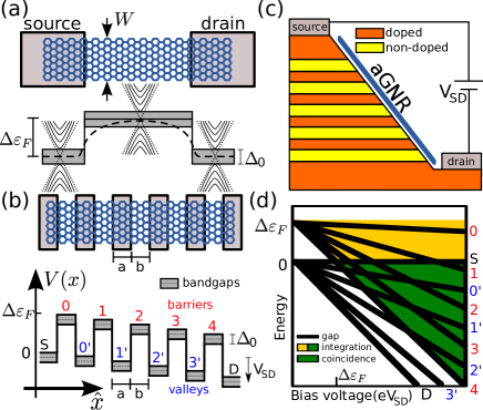
In this work we consider an -barrier superlattice potential on a semiconducting armchair graphene nanoribbon (aGNR); Fig. 1. The electronic structure of the aGNR is a quantized Dirac cone, due to the quantization of the transversal momentum , and can be metallic, , or semiconducting, , depending on the width of the nanoribbon; is the closest to zero transverse momenta. We choose , such that the aGNR is semiconducting with a bandgap meV; nm is the C-C distance. We use the transfer-matrix formalism to calculate the source-drain transmission coefficient across the superlattice potential along the aGNR, considering a finite bias voltage , revealing the electronic structure of the system; Fig. 2. The potential drop from source to drain follows a piecewise constant profile layer by layer; Fig. 1(b). The current is calculated within the usual Landauer-Büttiker formalism.
We find low bias NDR at zero and room temperatures within three distinct physical regimes. (i) For wide layers, the transmission across the bandgaps is strongly suppressed, and nearly unity for energies away from the bandgaps. With increasing voltage, both barrier and valley bandgaps split and cross as shown schematically in Fig. 1(d), showing, at the coincidence region, a pattern of diamond-shaped structures with alternating regions of finite and suppressed transmission, thus leading to NDR. For narrow barriers resonant tunneling across layers become relevant. (ii) At zero bias, hybridization of resonant modes leads to minibands with finite, nearly unity, transmission; Fig. 2(b)-2(e). At very low voltages meV (of the order of the miniband energy width) the resonant states misalign, thus breaking the minibands into off-resonance Wannier-Stark ladders with suppressed transmission. This gives rise to a single current spike near meV. (iii) With increasing , rungs of ladders from distinct minibands cross and hybridize, showing a new set of resonant spikes in , Fig. 2(a), thus leading to current spikes and NDR.
II Proposed system & model
The modulation of the Dirac cone into a superlattice potential can be achieved by different setups. It was shown that local charge-transfer effects between graphene and some metals (e.g., Al, Cu, Ag, Au, Pt) rigidly shifts the Dirac cone; Giovannetti et al. (2008); Vanin et al. (2010); Barraza-Lopez et al. (2010); Varykhalov et al. (2010) Fig. 1(a). A series of metallic stripes over graphene can create the proposed superlattice potential; Fig. 1(b). Equivalently, the same structure can be obtained by selectively doping graphene regions in an alternate fashion. Additionally, the aGNR could be arranged along the doped/non-doped layers of a cleaved semiconductor heterostructure; Krahne et al. (2002) Fig. 1(c). Narrow systems ( nm) are desirable to keep transport ballistic at room temperatures.
We consider low-energy excitations of graphene within the envelope function approximation, Wallace (1947); Neto et al. (2009) i.e., the graphene Dirac Hamiltonian. The finite size of the nanoribbon requires vanishing wave functions at the edges, where for aGNR both and sublattices of the honeycomb lattice are present. This leads to vanishing boundary conditions for the envelope functions at these edges. Neto et al. (2009) The validity of these boundary conditions is discussed in Ref. Brey and Fertig, 2006. Within this description, the electronic structure of an aGNR is a quantized Dirac cone, . Here for the conduction and valence bands, nm/s is the Fermi velocity, is the momentum in the longitudinal direction , is the quantized transverse momentum with integer , and nm. The fundamental gap is given by meV, with nm-1.
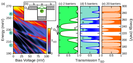
To calculate the transmission we use the transfer-matrix formalism, Datta (1997) which relates the coefficients of the incoming and outgoing plane waves at the source and drain leads across the superlattice layers (see the Appendix for details). We consider a piecewise constant superlattice potential along the direction, Figs. 1(b), through which the electronic structure of each layer is shifted by the local potential. In Figs. 2–4 we show only for , as it contains the major contribution for the current in all investigated cases.
The current density of Dirac electrons in graphene is given by , where the factor of accounts for the valley and spin degeneracies, is the envelope function spinor for the or valley, and are the Pauli matrices. Within the Landauer-Büttiker formalism, Datta (1997); Blanter and Buttiker (2000) the current reads
| (1) |
where and are the Fermi-Dirac distributions at the source and drain, and is the source chemical potential. We truncate the sum over to a few near .
III Results
In Fig. 2(b) we consider a narrow graphene well with nm and . The solution of the graphene Dirac equation within the bandgap region shows a confined state. Trauzettel et al. (2007) This state corresponds to the resonant spike within the region in Fig. 2(b) for two barriers. For barriers the confined states hybridizes into states, leading to minibands for large ; Figs. 2(c) and 2(d). The minibands away from the region occur due to reflections at each interface. For finite bias the minibands break into single resonant levels, Wannier-Stark ladders, as the confined modes from each layer misalign; Fig. 2(e). At the crossings of Wannier-Stark ladders from distinct minibands the transmission increases due to resonant tunneling.
NDR regimes
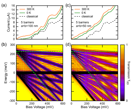
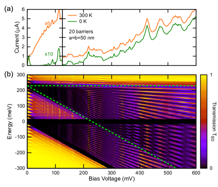
To contrast distinct NDR regimes in our system, we discuss the current-voltage characteristics - and the energy-voltage diagram for the following three cases. We compare five-barrier superlattices with (i) wide layers [Figs. 3(a) and 3(b)] and (ii) narrow layers [Figs. 3(c) and 3(d)]. We then discuss (iii) a 20-barrier superlattice with narrow layers; Fig. 4. The dashed lines in the diagrams delimit the zero-temperature window of integration for , defined between the source meV and drain chemical potentials.
III.0.1 “Classical” regime
For wide layers, nm, tunneling across bandgaps is strongly suppressed and the diagram, Fig. 3(b), follows closely the diamond pattern in Fig. 1(d). For meV the current increases monotonically as the barriers bandgaps misalign. At the coincidence region, meV, crossings of barrier and valley bandgaps lead to the diamond pattern of finite and suppressed . This alternation leads to the NDR near and mV, in Fig. 3(a). The intensity of the NDR in this regime increases with the layers width, as the tunneling across bandgaps becomes more suppressed. The dashed curve in Fig. 3(a) is calculated with the limiting case where tunneling is completely suppressed across bandgaps, i.e., across a bandgap, and otherwise. Note the similarity of the dashed classical line with the exact calculations in Fig. 3(a).
For narrow layers, nm in Figs. 3(c) and 3(d), the NDR due to classical regime is absent as it requires strong tunneling suppression. Interestingly, however, the diagram of a few narrow layers clearly shows the evolution of the zero-bias minibands into Wannier-Stark ladders with increasing ; Fig. 2(e). The Wannier-Stark ladders remain as individual transmission spikes while there is an overlap of barriers (or valley) bandgaps. For this condition is violated, and the tunneling across individual bandgaps dominate. At the crossings of barrier and valley bandgaps, resonant effects are still visible in the diagram as stripes, corresponding to confined states between the overlapping band gaps; see Fig. 3(d) near meV and mV.
III.0.2 Miniband regime
Considering a larger number of barriers, in Fig. 4, the aligned resonant modes hybridize into superlattice minibands; Fig. 2. If is located within the miniband, at low biases the current is dominated by the transmission across these resonant modes. As the bias increases, the modes misalign breaking up the miniband into Wannier-Stark ladders. For five barriers, Fig. 2(a), the rungs of the ladders shows nonresonant transmission peaks, and enhanced resonant transmission at crossings of the rungs (see Wannier-Stark ladder regime below). For 20 barriers, transmission through nonresonant rungs is strongly suppressed due to the larger number of bandgaps. At very low voltages, Fig. 4, the current initially increases with as the transport occurs through the miniband. Near meV (of the order of the miniband width) the miniband breaks up into the nonresonant rungs suppressing the current, thus resulting in a pronounced current peak.
III.0.3 Wannier-Stark ladder regime
With increasing bias, rungs from Wannier-Stark ladders of distinct minibands cross, Fig. 2(a), creating new resonances through the superlattice layers. For 20 barriers, where transmission from non-resonant rungs is strongly suppressed, the crossings show sharp stripes, e.g., at , , , and mV; Fig. 4(b). Each of these stripes, and others with lower contrast at smaller voltages, leads to current spikes in Fig. 4(a). The spikes broaden with increasing bias as the band gaps misalign. For meV, the crossings of broadened Wannier-Stark ladders from minibands near the barrier and valley bandgaps show diamond-shaped structures in the diagram, thus leading to a series of NDR spikes similar to the classical regime.
IV Conclusions
We have found that three distinct regimes can lead to NDR in semiconducting aGNR superlattices. (i) In the classical regime the NDR occurs as the bandgaps of different layers cross with increasing . (ii) For narrow layers and very low biases, meV, the transport is dominated by the resonant tunneling through the miniband, and the NDR occurs as the miniband breaks into Wannier-Stark ladders with increasing bias. (iii) For higher bias rungs of distinct ladders cross originating new resonances and current peaks. Interestingly, due to the high mobility of the carriers, we obtain low bias NDR peaks with high current densities.
Final remarks
The predicted NDR effects reported here are strictly valid for ballistic electronic transport through ideal aGNR superlattices. For relatively clean systems, however, we expect detrimental effects such as those induced by disorder, impurities and structural defectsAbedpour et al. (2009); Cheraghchi et al. (2011); Han et al. (2010); Saloriutta et al. (2011) to broaden the resonances in the - curves, thus possibly reducing the peak-to-valley current ratios. Interestingly, a recent calculation for the electronic transport through a single-barrier defined on a zigzag-terminated graphene nanoribbon shows evidence for a transport gap despite the gapless spectrum of the edge states of the system. Nakabayashi et al. (2009) Therefore, we expect that a superlattice defined on a zigzag graphene nanoribbon should exhibit transport features similar to those of the armchair case investigated here. The effects of edge irregularities, strong disorder, and interactions (even at the Hartree level) lie beyond the scope of the present work and deserve further study.
Acknowledgements.
We thank Björn Trauzettel, Saiful Khondaker, Volodymyr Turkowski, and Stephano Chesi for useful discussions. The authors acknowledge support from FAPESP, CNPq, Swiss NSF, and NCCR Nanoscience. M.N.L. acknowledges support from NSF (Grant No. ECCS-0725514), DARPA/MTO (Grant No. HR0011-08-1-0059), NSF (Grant No. ECCS-0901784), and AFOSR (Grant No. FA9550-09-1-0450).Appendix A Transfer Matrix
In this Appendix we detail the calculation of the transmission coefficient through the nanoribbon superlattice via the transfer-matrix approach. We describe the potential across the system as piecewise constant; Fig. 1(b). In each layer the potential is a constant . The superlattice potential is 0 for valleys, and mV for barriers (typical value obtained from Refs. Giovannetti et al., 2008; Vanin et al., 2010; Barraza-Lopez et al., 2010; Varykhalov et al., 2010). The second term is the potential energy drop across the layers due to the electric field, where is the coordinate of the center of the layer , and is the distance between the source and drain.
The solution of the Dirac equation in each layer ( and for the source and drain, and an integer for the intermediate layers) is given by the plane-wave spinorsKatsnelson et al. (2006); Neto et al. (2009) . For convenience we write the component in a matrix form , where the components of the spinor denote the coefficients of the outgoing and incoming plane waves. The matrix is
| (2) |
The eigenenergies in each layer are , with for the conduction band and for the valence band, is the longitudinal momentum in layer , is the quantized transversal momentum (conserved through the system), and .
The continuity of the spinors at the interfaces yields , where is the position of the interface between the layers and . Applying this matching throughout the system, we obtain a matrix equation connecting the coefficients from source and drain , where is the transfer matrix given by
| (3) |
The definition of the reflected and transmitted waves depends on the sign of the electron energy at source and drain , such that the source and drain coefficients are given by
| (6) | |||||
| (9) |
From the graphene Dirac Hamiltonian, the current density reads . At the stationary regime the current flow at source and drain is the same, requiring the match , from which we identify the transmission coefficient ,
| (10) |
This transmission coefficient as a function of the energy reveals the electronic structure of the system, in which the confined modes in between the layers show up as resonant spikes and minibands; Fig. 2.
References
- Novoselov et al. (2005) K. S. Novoselov, A. K. Geim, S. V. Morozov, D. Jiang, M. I. Katsnelson, I. V. Grigorieva, S. V. Dubonos, and A. A. Firsov, Nature (London) 438, 197 (2005).
- Katsnelson et al. (2006) M. I. Katsnelson, K. S. Novoselov, and A. K. Gaim, Nat. Phys. 2, 620 (2006).
- Neto et al. (2009) A. H. C. Neto, F. Guinea, N. M. R. Peres, K. S. Novoselov, and A. K. Gaim, Rev. Mod. Phys. 81, 109 (2009).
- Avouris (2010) P. Avouris, Nano Lett. 10, 4285 (2010).
- Yu and Cardona (2005) P. Y. Yu and M. Cardona, Fundamentals of Semiconductors (Springer, Berlin, 2005).
- Mortazawi et al. (1989) A. Mortazawi, V. Kesan, D. Neikirk, and T. Itoh, in Microwave Conference, 1989. 19th European (1989), pp. 715–718.
- Sollner et al. (1988) T. C. L. G. Sollner, E. R. Brown, W. D. Goodhue, and C. A. Correa, J. Appl. Phys. 64, 4248 (1988).
- Sze and Ng (2007) S. M. Sze and K. K. Ng, Physics of Semiconductor Devices (Wiley-Interscience, New York, 2007).
- Tsu (1973) R. Tsu, Appl. Phys. Lett. 22, 562 (1973).
- Sollner (1983) T. C. L. G. Sollner, Appl. Phys. Lett. 43, 588 (1983).
- Iogansen (1964) L. V. Iogansen, Sov. Phys. JETP 18, 146 (1964).
- Esaki and Tsu (1970) L. Esaki and R. Tsu, IBM J. Res. Develop. 14, 61 (1970).
- Tsu (2005) R. Tsu, Superlattice to Nanoelectronics (Elsevier, Amsterdam, 2005).
- Goldman et al. (1987) V. J. Goldman, D. C. Tsui, and J. E. Cunningham, Phys. Rev. Lett. 58, 1256 (1987).
- Bai and Zhang (2007) C. Bai and X. Zhang, Physical Review B 76, 075430 (2007).
- Brey and Fertig (2009) L. Brey and H. A. Fertig, Physical Review Letters 103, 46809 (2009).
- Park et al. (2009) C. H. Park, Y. W. Son, L. Yang, M. L. Cohen, and S. G. Louie, Physical Review Letters 103, 46808 (2009).
- Barbier et al. (2010) M. Barbier, P. Vasilopoulos, and F. M. Peeters, Physical Review B 81, 075438 (2010).
- Stojanović et al. (2010) V. M. Stojanović, N. Vukmirović, and C. Bruder, Physical Review B 82, 165410 (2010).
- Burset et al. (2011) P. Burset, A. L. Yeyati, L. Brey, and H. A. Fertig, Physical Review B 83, 195434 (2011).
- Guo et al. (2011) X. Guo, D. Liu, and Y. Li, Applied Physics Letters 98, 242101 (2011).
- Jiang et al. (2011) J. Jiang, J. Wang, and B. Wang, Applied Physics Letters 99, 043109 (2011).
- Abedpour et al. (2009) N. Abedpour, A. Esmailpour, R. Asgari, and M. R. Tabar, Physical Review B 79, 165412 (2009).
- Cheraghchi et al. (2011) H. Cheraghchi, A. H. Irani, S. M. Fazeli, and R. Asgari, Physical Review B 83, 235430 (2011).
- Giovannetti et al. (2008) G. Giovannetti, P. A. Khomyakov, G. Brocks, V. M. Karpan, J. van den Brink, and P. J. Kelly, Phys. Rev. Lett. 101, 026803 (2008).
- Vanin et al. (2010) M. Vanin, J. J. Mortensen, A. K. Kelkkanen, J. M. Garcia-Lastra, K. S. Thygesen, and K. W. Jacobsen, Phys. Rev. B 81, 081408(R) (2010).
- Barraza-Lopez et al. (2010) S. Barraza-Lopez, M. Vanević, M. Kindermann, and M. Y. Chou, Phys. Rev. Lett. 104, 076807 (2010).
- Varykhalov et al. (2010) A. Varykhalov, M. R. Scholz, T. K. Kim, and O. Rader, Phys. Rev. B 82, 121101 (2010).
- Wang et al. (2008) Z. F. Wang, Q. Li, Q. W. Shi, X. Wang, J. Yang, J. G. Hou, and J. Chen, Appl. Phys. Lett. 92, 133114 (2008).
- Do and Dollfus (2010) V. N. Do and P. Dollfus, J. Appl. Phys. 107, 063705 (2010).
- (31) A recent work (Ref. Dragoman and Dragoman, 2007) has claimed that low-bias NDR can be achieved with a single barrier in a infinite graphene sheet. This, however, has been disputed in Refs. Do, 2008; Do et al., 2008.
- Ren et al. (2009) H. Ren, Q.-X. li, Y. Luo, and J. Yang, Appl. Phys. Lett. 94, 173110 (2009).
- Habib et al. (2011) K. Habib, F. Zahid, and R. Lake, Applied Physics Letters 98, 192112 (2011).
- Fang et al. (2011) H. Fang, R. Wang, S. Chen, M. Yan, X. Song, and B. Wang, Applied Physics Letters 98, 082108 (2011).
- Krahne et al. (2002) R. Krahne, A. Yacoby, H. Shtrikman, I. Bar-Joseph, T. Dadosh, and J. Sperling, Appl. Phys. Lett. 81, 730 (2002).
- Wallace (1947) P. R. Wallace, Phys. Rev. 71, 622 (1947).
- Brey and Fertig (2006) L. Brey and H. A. Fertig, Phys. Rev. B 73, 235411 (2006).
- Datta (1997) S. Datta, Electronic Transport in Mesoscopic Systems (Cambridge University Press, Cambridge, England, 1997).
- Blanter and Buttiker (2000) Y. M. Blanter and M. Buttiker, Phys. Rep. 336, 1 (2000).
- Trauzettel et al. (2007) B. Trauzettel, D. V. Bulaev, D. Loss, and G. Burkard, Nat. Phys. 3, 192 (2007).
- Han et al. (2010) M. Han, J. Brant, and P. Kim, Physical review letters 104, 56801 (2010).
- Saloriutta et al. (2011) K. Saloriutta, Y. Hancock, A. Kärkkäinen, L. Kärkkäinen, M. J. Puska, and A. P. Jauho, Physical Review B 83, 205125 (2011).
- Nakabayashi et al. (2009) J. Nakabayashi, D. Yamamoto, and S. Kurihara, Physical Review Letters 102, 66803 (2009).
- Dragoman and Dragoman (2007) D. Dragoman and M. Dragoman, Appl. Phys. Lett. 90, 143111 (2007).
- Do (2008) V. N. Do, Appl. Phys. Lett. 92, 216101 (2008).
- Do et al. (2008) V. N. Do, V. H. Nguyen, P. Dollfus, and A. Bournel, J. Appl. Phys. 104, 063708 (2008).