Now at ]Instituto Madrileño de Estudios Avanzados en Nanociencia (IMDEA Nanociencia), Cantoblanco, 28049 Madrid, Spain.
On the magnetization textures in NiPd nanostructures
Abstract
We have observed peculiar magnetization textures in Ni80Pd20 nanostructures using three different imaging techniques: magnetic force microscopy, photoemission electron microscopy under polarized X-ray absorption, and scanning electron microscopy with polarization analysis. The appearances of diamond-like domains with strong lateral charges and of weak stripe structures bring into evidence the presence of both a transverse and a perpendicular anisotropy in these nanostrips. This anisotropy is seen to reinforce as temperature decreases, as testified by a simplified domain structure at 150 K. A thermal stress relaxation model is proposed to account for these observations. Elastic calculations coupled to micromagnetic simulations support qualitatively this model.
I Introduction
The nickel-palladium alloys (denoted here as NiPd), which form a solid solution over the whole concentration range, have been the subject of many studies for their magnetic properties. Sadron (1932); Néel (1932); Crangle and Scott (1965); Ferrando et al. (1972) Indeed, palladium is the 4d parent of nickel. It is close to being ferromagnetic according to the Stoner criterium, and forms a ferromagnetic alloy with nickel down to Ni atomic concentrations as small as %, Murani et al. (1974); Kontos et al. (2004) with a smoothly varying Curie temperature, Hansen (1958) due to its large magnetic polarizability. Vogel et al. (1997) Thus, in recent years, NiPd alloys have been used as ferromagnets of tunable strength for studying the ferromagnet-superconductor proximity effect. Kontos et al. (2001) Furthermore, Pd as a noble metal has been shown to provide good electrical contacts with carbon nanotubes, Javey et al. (2003) a property retained by the Ni rich phase, Sahoo et al. (2005a) so that Pd1-xNix () has been demonstrated to perform as a good spin injector and analyzer in the study of gated spin-transport in carbon nanotubes. Sahoo et al. (2005b); Man et al. (2006) For such studies, NiPd occurs in the form of nanostructures, in which the magnetization orientation is expected to be controlled by the nanostructure shape and the applied field.
With soft magnetic materials like NiFe, the magnetostatic energy (the so-called shape anisotropy) gives rise to a preferred orientation in the direction of the long edge of the nanostructure, with a coercive field that decreases as the nanostructure width increases, providing good control of the magnetization in the magnetic electrodes. For NiPd electrodes, however, this appears not to be the case. Sahoo et al. Sahoo et al. (2005a) indeed observed, when applying field along the length of the electrodes, a progressive magnetization reversal. The switching characteristics changed completely when applying field in the direction transverse to the electrodes, Feuillet-Palma et al. (2010) as explained by the first magnetic force microscopy images obtained at LPS that constitute the starting point of this work. In these two cases, the palladium atomic concentration was 25 % to 30 %. Additionally, anisotropic magnetoresistance (AMR) measurements performed on electrodes (with an estimated 40 % palladium content) showed that the magnetization was very far from the longitudinal orientation. Gonzalez-Pons et al. (2008) From a comparison of AMR signals measured for fields oriented along several directions, that study concluded moreover that the magnetization was, on the average, tilted out of the plane. The existence of a strong perpendicular anisotropy in infinite films was also directly confirmed by ferromagnetic resonance measurements, Gonzalez-Pons et al. (2008) and could also be guessed from the extraordinary Hall effect measurements on 90 % Pd rich samples. Kontos et al. (2001) In view of this complexity, we push here the study one step further by imaging the complex magnetization textures in the NiPd electrodes, using different magnetic imaging techniques with a high spatial resolution, namely magnetic force microscopy (MFM), photoemission electron microscopy combined with X-ray magnetic circular dichroism (XMCD-PEEM) and scanning electron microscopy with polarization analysis (SEMPA). The possibilities and characteristics of these techniques are indeed complementary: Hopster and Oepen (2005) we used MFM to get a global image of the structure with no depth or component resolution, XMCD-PEEM to probe the surface magnetization componentwise and also at low temperature, and SEMPA for vectorial maps of the surface magnetization. In order to interpret quantitatively the results obtained, an analysis based on the differential thermal expansion of film and substrate, including elastic and micromagnetic simulations, is proposed and discussed as a cause for the observed anisotropies.
II Imaging and qualitative analysis
The structures under study are Ni-rich NiPd nanostrips with varying widths from 100 nm to 1000 nm and thicknesses between 10 nm and 50 nm, the length being 5 m unless otherwise specified, with a 3 nm Pd or Al cap to protect against oxidation. They have been patterned using a lift-off technique, by e-beam lithography and e-gun UHV evaporation with deposition rate around nm/s, onto Si substrates with native oxide. The saturation magnetization ( A/m) and the typical composition have been measured by, respectively, alternating gradient force magnetometry (AGFM) and Rutherford back-scattering spectroscopy (RBS), giving an atomic composition of Pd of (slightly drifting with source usage). Note that the following results involve only the virgin magnetization states, but that a magnetic field has also been applied, showing that the magnetization textures under study are more robust than simple metastable states generated during growth.
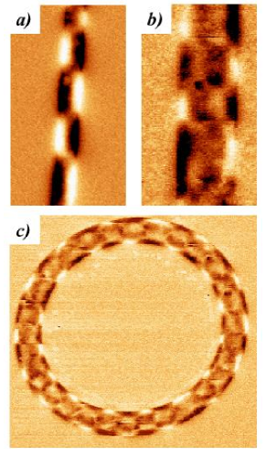
The MFM contrast of nm thick narrow strips (Fig. 1a) reveals alternate edge magnetic charges. A clear correlation between the two sides is also observed, with magnetic charges on one side facing opposite charges on the other. This rather uniform pattern corresponds to magnetic domains with a transverse magnetization, an orientation orthogonal to the longitudinal direction that minimizes the magnetostatic energy (shape anisotropy). For slightly wider strips (Fig. 1b), in addition to the edge magnetic charges, an inner contrast appears. This means that the magnetization does not fully lie along the transverse axis but potentially curls inside, revealing a more complex texture (also potentially perturbed by the stray field of the MFM tip). The generality of the transverse orientation is directly attested by the image of a ring-shape sample (Fig. 1c). Note also that no such magnetic structures were observed by MFM on the control unpatterned films. As MFM probes only the sample magnetic stray field (and on one side of the sample), magnetization distribution reconstruction from a MFM image is not unique. Therefore we used two other direct imaging techniques, namely XMCD-PEEM and SEMPA. Both techniques yield images of magnetization within a few nanometers from the surface.
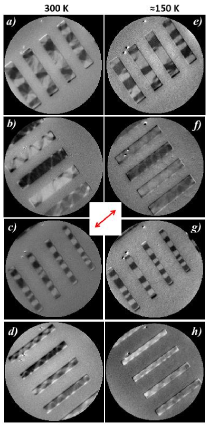
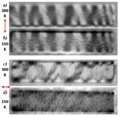
The XMCD-PEEM experiments were carried out with the combined PEEM-LEEM (low energy electron microscope) apparatus Locatelli et al. (2006) operating at the Nanospectroscopy beamline of the Elettra synchrotron, the X-rays being tuned to the edge of Ni. In the setup used, the circularly polarized X-rays impinge on the sample at a angle from the surface. The differential absorption of the X-rays (circular dichroism), proportional to the dot product of magnetization and photon wavevector, therefore predominantly originates from the in-plane magnetization components, with a small contribution from the out-of-plane component. The magnetization images are obtained by forming the difference of PEEM images acquired with opposite helicity of the X-rays. This method is inherently surface-sensitive due to the limited electron escape depth, which is a few nanometers for the typical 2 eV energy of the collected electrons. We show in Fig. 2 only the large (from m to m) and intermediate (from m to m) width nanostructures, for the medium thickness ( nm). Orthogonal sets of strips have been patterned, allowing us to probe on the same sample the transverse (Figs. 2a and 2c) and the longitudinal (Figs. 2b and 2d) components of magnetization, albeit on different structures. These magnetic images corroborate the conclusions drawn from the MFM images, as Figs. 2a and 2c show strong transverse components, with a higher complexity for the wider structures. On the other hand, a magnetic contrast is also present for images in the longitudinal configuration (Fig. 2b, 2d), proving that the magnetization is not fully transverse. For intermediate width (Fig. 2d) as well as narrower structures, symmetric diamond patterns are observed with no global longitudinal moment. However, deformed diamond patterns also appear (e.g. for 500 nm and 600 nm width in Fig. 2d), where closure domains on the long edges with one (longitudinal) magnetization are bigger than for the opposite magnetization, meaning that such structures have a non-zero longitudinal moment. For the large widths (Fig. 2b), this deformation is general, and very pronounced. Note however that the close proximity of the structures introduces a dipolar coupling, stabilizing a staggered (between successive nanostructures) longitudinal magnetization structure, quite apparent on Fig. 2b by the alternation of bright and dark overall contrasts. This dipolar coupling gives rise to a (staggered) applied field along the longitudinal direction.
At this point, magnetization vector maps of the structures are needed. With XMCD-PEEM, this requires an azimuthal sample rotation and accurate image matching. Instead, this is achievable using SEMPA, whereby images of the magnetization direction are obtained by measuring the spin polarization of secondary electrons emitted in the SEM. Two vector components (either the two in-plane, or one in-plane and the out of plane component) of the surface magnetization along with the conventional SEM image are acquired simultaneously using a quadrant spin detector. For these experiments, performed on the SEMPA at NIST, the sample surface was cleaned in situ by sputtering with 1 keV Ar ions (checked by Auger spectroscopy) and then capped with a few monolayers Fe for contrast enhancement. All images discussed in the following are maps of the surface magnetization distribution resolved along the in-plane (longitudinal) and (tranverse) axes.
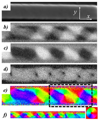
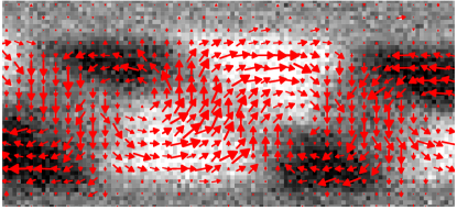
Fig. 3a displays a conventional SEM image of a m wide, nm thick and 10 m long nanostrip, attesting to the nanopatterning quality. The simultaneously measured in-plane components of the surface magnetization are shown in Figs. 3b and 3c, featuring the and distributions, respectively: the longitudinal image (Fig. 3b) shows the ‘closure’ domains, and the transverse image (Fig. 3c) shows the ‘diamond’ domains. Note that there is about 35 nm of longitudinal drift during the image scan, which adds to the slanted shape of domains. Fig. 3d is a composite image displaying , the magnitude of the in-plane magnetization. The contrast appears uniform in the image, with a noise level identical to that of the images of the two components, except at points roughly located along the strip axis. The latter clearly identify with the vortex cores, also noticeable in MFM images, yet indirectly. The alternate off-centered position of the vortices that is very visible in Fig. 3d is another indication of a non-zero longitudinal moment of the structure. Combining data in Figs. 3b and 3c allows for a vector representation of the in-plane magnetization (Fig. 3e). A magnified vector map superposed onto the longitudinal contrast is also shown in Fig. 4. Similar features are observed on wide strips (Fig. 3f).
In addition, we have observed that this transverse behaviour changes strongly with temperature, by comparing XMCD-PEEM images at room temperature (Figs. 2a to 2d) and at low temperature (, Figs. 2e to 2h) on the same structures. First, comparing the transverse component (Figs. 2a vs. 2e, and 2c vs. 2g), it is clear that the magnetic texture has been simplified when lowering temperature. The fact that intermediate grey levels have disappeared proves the reinforcement of the transverse anisotropy. This is corroborated by the loss of magnetic contrast while probing the longitudinal component (Figs. 2b vs. 2f, and 2d vs. 2h).
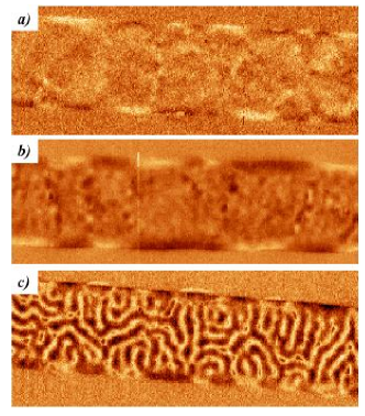
Moreover, at low temperature or for thicker structures ( nm), an additional contrast with a fine scale appears both in the longitudinal and transverse configurations (Fig 5; a similar contrast was also observed in SEMPA for the 50 nm structures at room temperature). This is the signature of a so-called weak stripe domain structure Hubert and Schäfer (1998), a fingerprint of an additional anisotropy with out of plane easy axis, with a magnitude that is smaller than the perpendicular demagnetization energy. In weak stripes, the magnetization at film center periodically tilts (less than ) out of the plane, in order to decrease the perpendicular anisotropy energy. The appearance of surface charges due to this perpendicular component is avoided by creating periodic ‘rolls’ for the magnetization components that are transverse to the main (in-plane) magnetization. Thus, the surface magnetization is mainly in-plane, with a periodic partial rotation towards the direction transverse to the stripe elongation. The wavevector of these periodic rotations is orthogonal to the main magnetization direction in order to avoid magnetic charges. In top view, weak stripes appear as domains running parallel to the main magnetization, with an oscillating transverse magnetization component (as well as with a smaller oscillating out-of-plane component with 90∘ dephasing). These weak stripes provide information about the magnetic structure and energetics of the sample. (i) As XMCD-PEEM essentially probes the in-plane magnetization component, the fluctuations due to the weak stripe structure reveal the mostly longitudinal stripes for transverse incidence and vice-versa. Thus, the observation of longitudinal weak stripes in the nanostrip center (Fig. 5b), and of transverse weak stripes over all the sample width, with a reinforcement of their contrast at the long edges of the structures (Fig. 5d), shows that the magnetization is globally transverse, with longitudinal components that are largest around mid-width. (ii) Even if weak stripes are barely observable at room temperature using XMCD-PEEM or SEMPA (not shown), MFM proves that they are already present (Fig. 6) when the thickness is large enough. This feature is traced back to the surface sensitivity of XPEEM or SEMPA, compared to the volume sensitivity of MFM. Thus, the critical thickness at which weak stripes appear can be estimated from the MFM images. Fig. 6 indeed shows that, whereas at 50 nm the stripe pattern is well established, at 30 nm nothing is observed, and at 40 nm some modulation is visible at some places, so that nm. This value will be later compared to calculations. (iii) Fig. 6c indicates that the transverse anisotropy dominates close to the edges since weak stripes meet the edges at right angles. Note that at these nanostrip dimensions, it is still possible to observe the bright and dark edge contrast, yet with no correlation anymore between the two sides. (iv) The fact that the surface magnetic contrast of the weak stripes increases at low temperatures reveals an increase of perpendicular anisotropy with respect to the demagnetizing energy.
To sum up these observations, a transverse anisotropy, competing with demagnetising energy, has to be invoked in order to maintain a stable diamond-like magnetic structure. In addition, we noted the presence of perpendicular anisotropy sufficient to allow for a weak stripe pattern to appear for nm thick nanostrips. Both contributions are enhanced when temperature is decreased.
III Quantitative analysis
We now discuss the origin of both transverse and perpendicular anisotropies. First, we note that the orientation of the long axis of the strips, relative either to the substrate or a deposition angle, has no noticeable effect on the observed magnetization texture. Considering the out-of-plane and edge-localised transverse anisotropies, the evolution of the magnetic contrast with temperature, and the independence of the effect on the orientation of the nanostructures (Fig. 1c), thermal stresses are a likely cause to all these phenomena. Indeed, metals and semiconductors have very different thermal expansion coefficients , for example K-1 and K-1. Assuming that the temperature during layer deposition is higher than room temperature (the sample holder was not cooled), a thermal stress exists in the NiPd layer at room temperature, that is reinforced at low temperature ().
In order to evaluate quantitatively this effect, the elastic problem in 2D (infinite nanostrip length) was numerically solved, for different nanostrip transverse dimensions. This was performed with a homemade finite differences code, in the framework of isotropic elasticity. Interpolated values for the elastic coefficients of NiPd were adopted, namely Young’s modulus GPa and Poisson’s ratio Yamamoto (1951); Rayne (1960). Figs. 7a to 7c show the strain components distribution across the section of a 30 nm thick and 500 nm wide nanostrip, assuming an infinitely rigid substrate. At the top edges, the NiPd is fully relaxed, noticeable on the and maps by the zero strain regions (see color code). Along the cross-section symmetry plane, the behaviour is the same as that expected for an infinite film, i.e. and . Here, is the initial interfacial strain, i.e. the product of the thermal expansion coefficient difference and the temperature difference , and is the perpendicular strain in an infinite film (both numbers are defined positive, but as temperature is lower than that during growth the film is in compression along the out-of-plane direction and in tension in-plane). Besides, one can note a very localised non-zero shear strain at the bottom edges of the nanostrip (Fig. 7c), that corresponds to the inclination of the lateral edge of the nanostrip.
Once the strains are known, considering the isotropic magnetoelastic coupling with a negative magnetostriction coefficient ( for Ni), it is possible to compute an anisotropy distribution map (Fig. 7d). Note that, because of the existence of shear, the magnetoelastic energy must be diagonalised at every location in order to get the local easy axis direction and anisotropy constants.
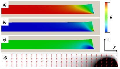
Since is negative, the easy axis lies along the compression axis, i.e. perpendicular to the sample plane in the middle (Fig. 7d) as already measured for Ni rich films. Ben Youssef et al. (2004) The finite size of the strips allows strain relaxation at the edges with the appearance of shearing, driving the easy axis to locally rotate towards the transverse direction. Therefore, thermal strains do lead to out-of-plane and transverse anisotropies, that vary with position, the transverse anisotropy being a ‘side-effect’ of the perpendicular anisotropy. In addition, the average value of the latter will depend on the aspect ratio of the strip cross-section since it rests on edge contributions. This dependence is supported by indirect magnetization measurements of some nanostrips by anisotropic magnetoresistance measurements (not shown).
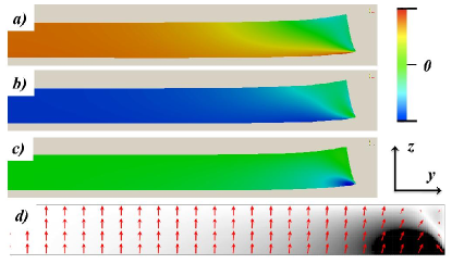
The elastic calculations were repeated for a deformable substrate, and the results are shown in Fig. 8. The deformations in the NiPd layer are reduced, as one part of the thermal stress is relaxed in the substrate. As a result, the induced anisotropy is also reduced, keeping roughly the same distribution.
The next step is to quantify the perpendicular anisotropy constant . The appearance of the weak stripe domains provides information about this constant since the critical thickness () for this depends on the quality factor . Hubert and Schäfer (1998); Vukadinovic et al. (2001) In the present case, is about nm. Considering an exchange constant of J/m, we obtain an exchange length of nm. Then, from results due to Vukadinovic et al., Vukadinovic et al. (2001) the quality factor’s critical value is , corresponding to a perpendicular anisotropy constant J/m3. This value is of the same order of magnitude as previously obtained by FMR for infinite films. Gonzalez-Pons et al. (2008) The anisotropy can be linked to a difference of temperature via the following relation (valid for an infinite film):
| (1) |
Therefore, K is needed to reach the required value, when considering an isotropic elastic constant GPa and for nickel. Yamamoto (1951) However, if we consider reported values for bulk NiPd with 20 % Pd, namely K Masumoto and Sawaya (1970) and , Tokunaga and Fujiwara (1978) and use the interpolated values for the elastic coefficients used in the calculations, we obtain a lower value K.
The calculated 2D anisotropy distributions were used as inputs into the OOMMF software OOM to simulate the equilibrium magnetic structures as a function of nanostrip dimensions. Keeping a 5 m long strip as in the experiments, the simulation started with 11 transverse magnetic domains (as observed), and with a noise of on the magnetization direction in order to avoid metastable states. Note that the anisotropy distribution, obtained for an infinitely long strip by a 2D calculation, is not correct at the ends of the structures, so that only the internal structures should be considered. For a nm thick nanostrip, weak stripe domains appeared (not shown), as expected.
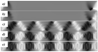
Fig. 9 presents the converged magnetic configurations in a m wide and nm thick nanostrip for different values of (calculated using the parameters of nickel; they would be 1.4 times smaller with the parameters of NiPd considered here). The calculations assumed the room temperature NiPd parameters; only the magnitude of the thermal stress induced anisotropy was scaled when changing the temperature difference . Whereas for K (a) and up to K (b) the domain initial state eventually becomes fully longitudinal, from K (c, d) a domain structure very similar to that experimentally observed is obtained, namely a diamond-like pattern together with off-centered vortex cores. However, the weak stripe domain structure is already visible in the simulation contrary to experiments, revealing that the computed perpendicular anisotropy is too strong compared to the transverse term. At still higher values, for K (e), a domain structure with essentially transverse domains develops, but also with very visible weak stripes. Thus, the observed structures are reproduced, but at the expense of large temperature differences, resulting in a relatively too strong perpendicular anisotropy.
IV Conclusion and perspectives
In this study, the magnetization distribution of NiPd nanostrips has been imaged using complementary techniques (MFM, XMCD-PEEM and SEMPA), revealing a transverse orientation of the magnetization and the appearance of weak stripes at low temperature or large thickness. The direct observation of a largely transverse magnetization differs from the conclusions previously drawn from AMR measurements only. Gonzalez-Pons et al. (2008) It however corresponds well with the effect of field orientation on the switching of NiPd electrodes observed in magneto-transport measurements on carbon nanotubes, as reported by Refs. Sahoo et al., 2005a; Feuillet-Palma et al., 2010. From these observations, it appears that in order to account for the observed textures, non-negligible out-of-plane and transverse anisotropies have to be present.
Considering the evolution with temperature (increase of both anisotropy constants as temperature decreases), a thermal stress mechanism has been considered as the origin of this surprising magnetization texture, via magnetostriction. Note that the same mechanism was invoked for explaining the spin reorientation transition observed in Ni1-xPdx alloys grown on Cu3Au(100). Matthes et al. (2002) Performing elastic, magneto-elastic and micromagnetic simulations, all qualitative features of the experiments could be reproduced, however with a disagreement regarding the relative magnitudes of the transverse and out-of-plane anisotropies.
We conclude that in addition, another effect may be present, such as an interfacial strain due to metal-substrate mismatch, a structural ordering of the alloy in the growth direction (i.e., the film normal), or a plastic strain relaxation. The latter effect may also explain the observed difference in magnetic properties between the infinite film and the nanostructures, at the same thickness. Indeed, weak stripes were seen to appear at lower thickness in the nanostructures, and the value of the perpendicular anisotropy measured by ferromagnetic resonance on infinite films was smaller than what was deduced for nanostructures of the same thickness. This shows also that the evaluation of strain in nanostructures is difficult, and that magnetic patterns in nanostructures made out of magnetostrictive materials should be imaged.
Even though only one composition has been considered in this study, the discussion is general and should apply to other Pd concentrations. For lower nickel concentrations, the thermal strain is anticipated to increase, as well as the Young’s modulus and magnetostriction constant (initially at least), resulting in a fairly constant induced anisotropy. On the other hand, the alloy magnetization will decrease, down to zero, so that the role of the anisotropy induced by the thermal strain will be more and more important as the nickel content decreases. As a result, the easy axis will switch to the direction perpendicular to the plane, at a temperature that depends on composition. This corresponds well to the observations at a Ni atomic concentration of 10 %. Kontos et al. (2001)
Finally, similar phenomena should occur for nanostructures made of other materials with a large magnetostriction and a small saturation magnetization.
V Acknowledgements
We thank T. Kontos and M. Aprili for discussions, encouragements and help in the sample elaboration, R. Weil for advice and help on sample nanofabrication, J. Ben Youssef and V. Castel for their help in samples characterization, F. Glas for the first estimations of the elastic deformations, and I. Vickridge at the SAFIR instrument for sample composition measurements by RBS. Work at LPS was partly supported by the Agence nationale de la Recherche, under contract ANR-09-NANO-002 HYFONT.
References
- (1)
- Sadron (1932) C. Sadron, Ann. physique (Paris), Series 10, 17, 371 (1932), Ph. D. thesis, Strasbourg (1932).
- Néel (1932) L. Néel, Ann. physique (Paris), Series 10, 17, 5 (1932), Ph. D. thesis, Strasbourg (1932).
- Crangle and Scott (1965) J. Crangle and W. Scott, J. Appl. Phys. 36, 921 (1965).
- Ferrando et al. (1972) W. Ferrando, R. Segnan, and A. Schindler, Phys. Rev. B 5, 4657 (1972).
- Murani et al. (1974) A. P. Murani, A. Tari, and B. R. Coles, J. Phys. F : Metal Phys. 4, 1769 (1974).
- Kontos et al. (2004) T. Kontos, M. Aprili, J. Lesueur, X. Grison, and L. Dumoulin, Phys. Rev. Lett. 93, 137001 (2004).
- Hansen (1958) M. Hansen, Constitution of Binary Alloys (McGraw-Hill Book Company, 1958).
- Vogel et al. (1997) J. Vogel, A. Fontaine, V. Cros, F. Pétroff, J.-P. Kappler, G. Krill, A. Rogalev, and J. Goulon, Phys. Rev. B 55, 3663 (1997).
- Kontos et al. (2001) T. Kontos, M. Aprili, J. Lesueur, and X. Grison, Phys. Rev. Lett. 86, 304 (2001).
- Javey et al. (2003) A. Javey, J. Guo, Q. Wang, M. Lundstrom, and H. Dai, Nature 424, 654 (2003).
- Sahoo et al. (2005a) a!L author S. Sahoo, T. Kontos, C. Schönenberger, and C. Sürgers, Appl. Phys. Lett. 86, 112109 (2005a).
- Sahoo et al. (2005b) S. Sahoo, T. Kontos, J. Furer, C. Hoffmann, M. Gräber, A. Cottet, and C. Schönenberger, Nature Phys. 1, 99 (2005b).
- Man et al. (2006) H. T. Man, I. J. W. Wever, and A. F. Morpurgo, Phys. Rev. B 73, 241401(R) (2006).
- Feuillet-Palma et al. (2010) C. Feuillet-Palma, T. Delattre, P. Morfin, J. M. Berroir, G. Feve, D. C. Glattli, B. Plaçais, A. Cottet, and T. Kontos, Phys. Rev. B 81, 115414 (2010).
- Gonzalez-Pons et al. (2008) J. C. Gonzalez-Pons, J. J. Henderson, E. del Barco, and B. Ozyilmaz, Phys. Rev. B 78, 012408 (2008).
- Hopster and Oepen (2005) H. Hopster and H. P. Oepen, Magnetic microscopy of nanostructures (Springer Verlag, Berlin, 2005).
- Locatelli et al. (2006) A. Locatelli, L. Aballe, T. Mentes, M. Kiskinova, and E. Bauer, Surf. Interface Anal. 38, 1554 (2006).
- Hubert and Schäfer (1998) A. Hubert and R. Schäfer, Magnetic Domains (Springer Verlag, Berlin, 1998) pp. 298–303.
- Yamamoto (1951) M. Yamamoto, Science reports of the research institutes, Tohoku Univ., Ser. A 3, 308 (1951), available at http://hdl.handle.net/10097/26440.
- Rayne (1960) J. Rayne, Phys. Rev. 118, 1545 (1960).
- Ben Youssef et al. (2004) J. Ben Youssef, N. Vukadinovic, D. Billet, and M. Labrune, Phys. Rev. B 69, 174402 (2004).
- Wortman and Evans (1965) J. Wortman and R. Evans, J. Appl. Phys. 36, 153 (1965).
- Vukadinovic et al. (2001) N. Vukadinovic, M. Labrune, J. Ben Youssef, A. Marty, J. C. Toussaint, and H. Le Gall, Phys. Rev. B 65, 054403 (2001).
- Masumoto and Sawaya (1970) H. Masumoto and S. Sawaya, Trans. J. I. M. 11, 391 (1970).
- Tokunaga and Fujiwara (1978) T. Tokunaga and H. Fujiwara, J. Phys. Soc. Japan 45, 1232 (1978).
- (27) OOMMF is a free software (in fact, an open framework for micromagnetics routines) developped by M.J. Donahue and D. Porter mainly, from NIST. It is available at http://math.nist.gov/oommf.
- Matthes et al. (2002) F. Matthes, M. Seider, and C. Schneider, J. Appl. Phys. 91, 8144 (2002).