Band structures of Cu2ZnSnS4 and Cu2ZnSnSe4 from many-body methods
Abstract
We calculate the band structures of kesterite and stannite Cu2ZnSnS4 and Cu2ZnSnSe4, using a state-of-the-art self-consistent approach. Our accurate quasiparticle states allow to discuss: the dependence of the gap on the anion displacement; the key-role of the non-locality of the exchange-correlation potential to obtain good structural parameters; the reliability of less expensive hybrid functional and GGA+U approaches. In particular, we show that even if the band gap is correctly reproduced by hybrid functionals, the band-edge corrections are in disagreement with self-consistent GW results, which has decisive implications for the positioning of the defect levels in the band gap.
Thin-film solar cells made of Cu(In,Ga)Se2 (CIGS) ally cost reduction and high efficiency, and compete today as successors of the dominating silicon technology. Nevertheless, there are concerns about their large scale production due to the increasing price of In and Ga. Quaternary chalcogenides Cu2ZnSn(S,Se)4 (CZTS) have recently been proposed as alternative absorbers. Their crystal structures and electronic properties are very similar to those of the parent CIGS, while their constituent elements are naturally abundant and non-toxic. The alloys Cu2ZnSnSxSe1-x have optimal gaps according to the Shockley-Queisser limit and their use as absorbers in thin film solar cells is getting established by a growing energy conversion efficiency (almost 10% todorov10 ; redinger11 for lab cells). However, the understanding of the properties of the different phases of Cu2ZnSnS4 and Cu2ZnSnSe4is still rather superficial, and only few recent studies have addressed their structural persson10 ; chen09 ; chen10bis , electronic chen09 ; persson10 ; paier09 , and defect properties chen10 ; nagoya10 .
The zincblende-derived kesterite structure () of CZTS is recognized to be the most stable. The energy difference per atom with respect to the stannite structure () is only of few meV per atom persson10 ; chen09 ; chen09bis , proving that kesterite and stannite phases can coexist in experimental samples, and explaining the reported disordered structures schorr07 . Similarly to chalcopyrites CIGS, quaternary kesterite and stannite CZTS are obtained from the zincblende structure by replacing the Zn cations in such a way that each anion (Se or S) is coordinated by one Zn, one Sn and two Cu atoms. The existence of three distinct cations results in three different cation-anion bond lengths, which induce a displacement of the anion from its ideal zincblende site. That distortion is measured by the anion displacement parameters (, , ), i.e., the relative coordinates of the anion in the conventional body-centered tetragonal cell. The anion displacement is harder to measure than the lattice constants and , due to the inhomogeneity of the samples. Indeed, the dispersion of data for is known to be large in CIGS compounds jaffe84 ; merino96 . Concerning CZTS, fewer measurements can be found in literature and in most cases only and are reported exp-geo . Concerning the experimental band gaps kes-S-gaps ; stan-S-gaps ; ahn10 , early studies suggested a value of about 1.4–1.6 eV both for S and Se compounds. This was in disagreement with density functional theory (DFT) calculations chen09 ; persson10 , using semi-local or hybrid functionals, which obtained systematically a smaller gap for Se compounds. More recent measurements ahn10 delineate a gap of about 1 eV for Cu2ZnSnSe4, explaining the previous overestimation with the presence of ZnSe in the sample.
Note that the current workhorse ab initio theory is, in fact, DFT, in combination with the local density approximation (LDA) or generalized gradient approximations (GGA). However, this approach is totally inadequate to study the electronic structure of materials where the band gap is controlled by the hybridization of the states of a transition metal with states, such as in CIGS or Cu2ZnSnS4. Moreover the anion-cation bonds can be poorly described, leading to anion displacements outside the experimental range, even if lattice constants are as usual well reproduced. In particular, for CuIn(S,Se)2, LDA and GGA yield structural internal parameters with an error of about 5% for jaffe84 ; merino96 ; vidal10 . Such an error leads to an underestimate by more than 50% of the band gap in a calculation at the theoretical geometry vidal10 .
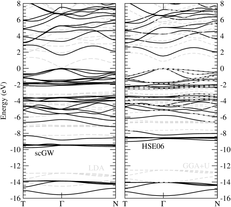
In this letter, we solve these problems by using state-of-the-art ab initio approaches that go beyond standard DFT to determine accurate quasiparticle band structures of both kesterite and stannite Cu2ZnSnS4 and Cu2ZnSnSe4. These calculations are based on a restricted self-consistent (sc) scheme, which has the advantage of being independent of the starting point (i.e., the poor LDA Kohn-Sham states) at the price of a larger computational complexity. Such approach, that we will refer to as sc, consists in performing a self-consistent calculation within the Coulomb hole plus screened exchange (COHSEX) approximation hedin , followed by a perturbative on top of it. This method has been applied to many transition-metal compounds, yielding excellent results for the band gaps and the quasiparticle band structure bruneval ; vidal10 ; vidal10bis . Standard LDA or GGA, and sc calculations were performed using the code ABINIT. We included semicore states in the valence to build the norm-conserving pseudopotentials for Cu, Zn and Sn. We also used the code VASP vasp for Heyd-Scuseria-Ernzerhof (HSE06)HSE06 hybrid functional and GGA+U calculations. Due to the similarity of CZTS materials with the CIGS family, the convergence parameters turned out to be the same reported in Refs. vidal10, .
In Fig. 1 we display band structures for kesterite Cu2ZnSnS4, obtained using different theoretical schemes at the experimental geometry exp-geo . In the left panel, the Kohn-Sham LDA band structure is compared with the sc bands. We observe that sc corrections upshift almost rigidly the lowest conduction states. Concerning the valence: (i) the dispersion of the S –Cu antibonding states at the top of the valence remains fairly unaltered, even if the overlap of LDA and quasiparticle wavefunctions shows remarkable variations in this region. (ii) The band width of the S –Cu bonding states (located between -3.5 and -6.7 eV) slightly increases. (iii) The bands associated to the (Zn,Sn)-S bond (between -8 and -10 eV) are inverted and downshifted by about 2 eV with respect to LDA. (iv) Also the S states are moved down by about 2 eV. In the right panel of Fig. 1 we show the same bands as obtained from GGA+U and HSE06 calculations. In this case HSE06 bands are remarkably similar to sc bands. This is not particularly surprising as the Hartree-Fock mixing of HSE06 is particularly suited for materials with gaps of about 1–2 eV paier08 ; marques11 . As expected, GGA+U shifts down the states with Cu character, thereby opening the gap to a reasonable value. However, it is evident from the figure, that the overall description of the band dispersions is quite inaccurate.
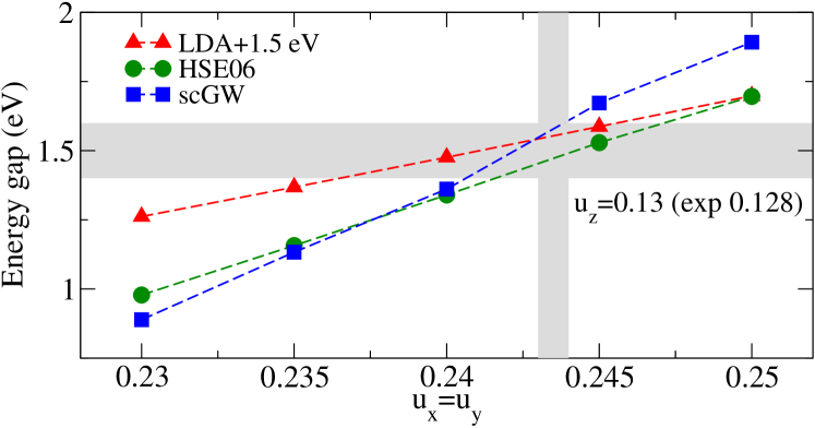
It is by now known that the band gap in CIGS materials is extremely sensitive to structural distortions jaffe84 and the remarkable stability of the band gap found experimentally can only be explained by compensating effects induced by intrinsic defects vidal10 . In order to establish if a similar behavior is also found in CZTS compounds, we performed calculations for kesterite (see Fig. 2) and stannite Cu2ZnSnS4 by varying the anion displacements. We also verified that sensible variations of and lattice parameters have negligible effects on the gap, in analogy to the case of CIGS vidal10 . We observe a strong variation of the band gap with , which is due to similar variations of both valence and conduction band edges. Note that the position of the top valence has important implications for the formation energies of charged defects. The slopes are substantially larger for sc calculations than for DFT-LDA, and even than for HSE06. In fact, they are controlled by the screening, which is essential to include in a self-consistent way, as in sc.
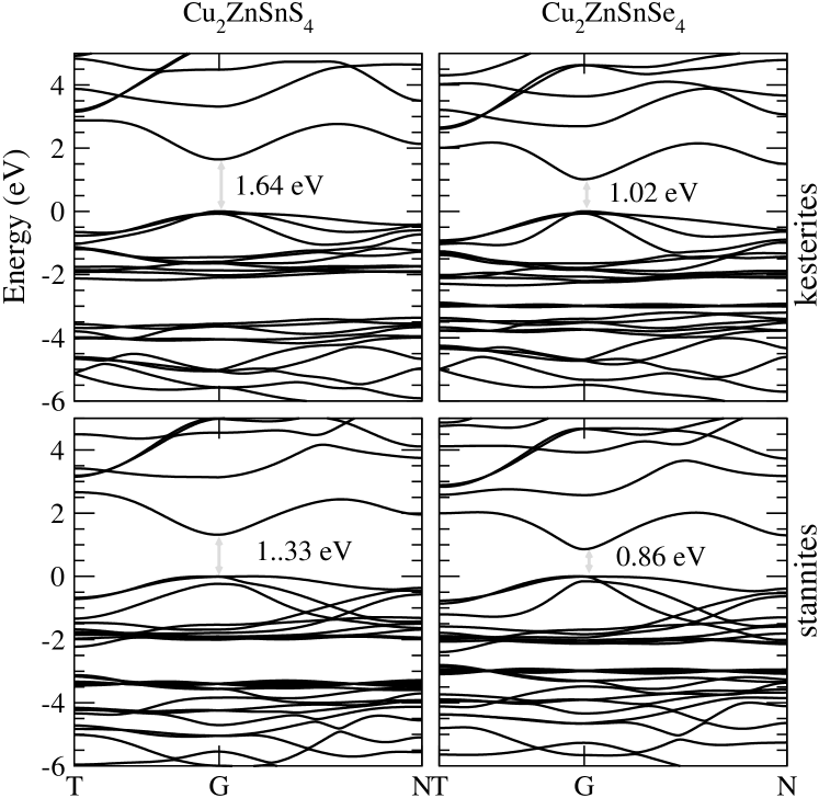
In Fig. 3 we can see the sc band structures of the four compounds of the CZTS family. For the kesterite Cu2ZnSnS4 and stannite Cu2ZnSnSe4 the experimental geometries were used exp-geo . For the remaining compounds, the experimental anion displacements are not reported exp-geo , and it was therefore necessary to resort to the theoretical structures. In view of the strong variation of the gap mentioned before, the choice of the theoretical framework for the geometry optimization is essential. In fact, we verified that LDA/GGA relaxed structures lead to unacceptably large errors (up to 40%) in the sc band gap, essentially related to the error in : Cu–(S,Se) and Zn–(S,Se) bond lengths are too small in DFT-LDA, while Sn–(S,Se) bond lengths are too large. The solution to this issue relies on the use of the HSE06 functional, that yields extremely accurate values for and the cell parameters, thanks to a better description of the localized states participating in the bonds. The major difference among the four band structures of Fig. 3 is the width of the band gaps, which are in excellent agreement with experimental results. As in the CIGS family, the Se compounds have a smaller gap with respect to the S ones. Furthermore, stannites have consistently smaller gaps than kesterites.
| LDA | GGA+U | HSE | sc | exp. | |||
| kesterite | S | 0.09 | 0.86 | 1.52 | 1.64 | 1.4–1.6 kes-S-gaps | |
| 0.00 | -0.52 | -0.81 | -0.49 | ||||
| Se | -0.24 | 0.34 | 0.94 | 1.02 | 0.8–1.0 ahn10 | ||
| 0.00 | -0.27 | -0.55 | -0.31 | ||||
| stannite | S | -0.11 | 0.63 | 1.27 | 1.33 | 1.4–1.5 stan-S-gaps | |
| 0.00 | -0.53 | -0.80 | -0.42 | ||||
| Se | -0.41 | 0.15 | 0.75 | 0.87 | 0.8–1.0 ahn10 | ||
| 0.0 | -0.28 | -0.56 | -0.35 |
Finally, in table 1 we show the band gaps and the top valence shifts with respect to DFT-LDA, obtained by aligning the average electrostatic potential in the different theoretical schemes. The validity of this alignment scheme is discussed in Ref. pasquarello, . Band edge-shifts are essential quantities to determine the position of defect levels in the gap and band offsets at interfaces. The most striking feature is that, even if HSE06 gives very good band gaps, the top valence and bottom conduction bands are systematically too low. These results suggest that the fact that hybrids (and more in general tuned hybrids) can give good gaps, does not mean that they always are able to reproduce correctly band-edge shifts pasquarello . We observe also that the valence band shift in GGA+U is close to the one obtained using sc, despite the underestimation of the gap. Note however, that GGA+U does not account for the dependence on of the valence-band shift, that is particularly strong in this family.
In conclusion, we obtained from many-body calculations a very accurate description of the electronic properties of the CZTS family. We proved that the HSE06 hybrid functional offers a good compromise between accuracy and computational cost, yielding good gaps and relaxed structures. Nevertheless, it cannot assure a reliable description of the valence and conduction contributions to the band-edge corrections, which has decisive implications for the position of the defect levels in the corrected band gap.
Furthermore we found a remarkable similarity between the electronic properties of the stannites and kesterite compounds, and to a large extent between these and the CIGS family. This once more points to the direction that CZTS materials are excellent candidates to replace the more costly CIGS in the absorbing layer of thin film photovoltaic cells.
SB acknowledges support from EUs 7th Framework Programme (e-I3 contract ETSF), and MALM from the French ANR (ANR-08-CEXC8-008-01). Calculations were performed at GENCI (project x2010096017).
References
- (1) K. Todorov, K. B. Reuter, and D. B. Mitzi, Adv. Mater. 22, E156 (2010).
- (2) A. Redinger, D. M. Berg, P. J. Dale, and S. Siebentritt, J. Am. Chem. Soc. 133, 3320 (2011).
- (3) C. Persson, J. of Appl. Phys. 107, 053710 (2010).
- (4) S. Chen, X. G. Gong, A. Walsh, and S.-H. Wei, Appl. Phys. Lett. 94, 041903 (2009).
- (5) S. Chen, A. Walsh, Y. Luo, J.-H. Yang, X.G. Gong, and S.-H. Wei, Phys. Rev. B 82, 195203 (2010).
- (6) J. Paier, R. Asahi, R. Wahl, and G. Kresse, Phys. Rev. B 79, 115126 (2009).
- (7) S. Chen, X. G. Gong, A. Walsh, and S.-H. Wei, Appl. Phys. Lett. 96 021902 (2010); S. Chen, J.-H. Yang, X. G. Gong, A. Walsh, and S.-H. Wei, Phys. Rev. B 81, 245204 (2010).
- (8) A. Nagoya, R. Asahi, R. Wahl, and G. Kresse, Phys. Rev. B 81, 113202 (2010).
- (9) S. Chen, X. G. Gong, A. Walsh, and S.-H. Wei, Phys. Rev. B 79, 165211 (2009).
- (10) S. Schorr, Thin Solid Films 515 (2007).
- (11) J. E. Jaffe and A. Zunger, Phys. Rev. B 29, 1882 (1984).
- (12) J. M. Merino, J. M. de Vidales, S. Mahanty, R. Díaz, F. Rueda, and M. Léon, J. Appl. Phys. 80, 5610 (1996).
- (13) S. R. Hall, J. T. Szymanski, and J. M. Stewart, Can. Mineral. 16, 131 (1978); H. Hahn and H. Schulze, Naturwiss. 52, 426 (1965); G. S. Babu, Y. B. K. Kumar, P. U. Bhaskar, and V. S. Raja, Semicond. Sci. Technol. 23, 085023 (2008); D. Olekseyuk, L. D. Gulay, I. V. Dydchak, L. V. Piskach, O. V. Parasyuk, and O. V. Marchuk, J. Alloys Compd. 340, 141 (2002).
- (14) H. Katagiri, K. Saitoh, T. Washio, H. Shinohara, T. Kurumadani, and S. Miyajima, Sol. Energy Mater. Sol. Cells 65, 141 (2001); J.-S. Seol, S.-Y. Lee, J.-C. Lee, H.-D. Nam, and K.-H. Kim, Sol. Energy Mater. Sol. Cells 75, 155 (2003); T. Tanaka, T. Nagatomo, D. Kawasaki, M. Nishio, Q. Guo, A. Wakahara, A. Yoshida, and H. Ogawa, J. Phys. Chem. Solids 66, 1978 (2005); N. Kamoun, H. Bouzouita, and B. Rezig, Thin Solid Films 515, 5949 (2007);
- (15) N. Nakayama and K. Ito, Appl. Surf. Sci. 92, 171 (1996); J. Zhang, L. Shao, Y. Fu, and E. Xie, Rare Metals 25, 315 (2006).
- (16) S. Ahn et al., Appl. Phys. Lett. 97, 021905 (2010) and references therein.
- (17) J. Vidal, S. Botti, P. Olsson, J.-F. Guillemoles, and L. Reining, Phys. Rev. Lett. 104, 056401 (2010).
- (18) L. Hedin and S. Lundqvist, Solid State Phys. 23, 1 (1970).
- (19) F. Bruneval, N. Vast, and L. Reining, Phys. Rev. B 74, 045102 (2006);
- (20) J. Vidal, F. Trani, F. Bruneval, M. A. L. Marques, and S. Botti, Phys. Rev. Lett. 104, 136401 (2010).
- (21) G. Kresse and J. Furthmüller, Comput. Mater. Sci. 6, 15 (1996).
- (22) J. Heyd, G. E. Scuseria, and M. Ernzerhof, J. Chem. Phys. 118, 8207 (2003); 124, 219906(E) (2006).
- (23) J. Paier, M. Marsman and G. Kresse, Phys. Rev. B 78, 121201 (2008).
- (24) M. A. L. Marques, J. Vidal, M. J. T. Oliveira, L. Reining, S. Botti, Phys. Rev. B 83, 035119 (2011).
- (25) A. Alkauskas, P. Broqvist, and A. Pasquarello, Phys. Status Solidi B, 248, 775 (2011).