High-Transconductance Graphene Solution-Gated Field Effect Transistors
Abstract
In this work, we report on the electronic properties of solution-gated field effect transistors (SGFETs) fabricated using large-area graphene. Devices prepared both with epitaxially grown graphene on SiC as well as with chemical vapor deposition grown graphene on Cu exhibit high transconductances, which are a consequence of the high mobility of charge carriers in graphene and the large capacitance at the graphene/water interface. The performance of graphene SGFETs, in terms of gate sensitivity, is compared to other SGFET technologies and found to be clearly superior, confirming the potential of graphene SGFETs for sensing applications in electrolytic environments.
pacs:
81.05.ue,07.07.Df,85.30.TvDue to its extraordinary chemical and electrochemical properties,Tang et al. (2009) graphene is a promising candidate for sensing in electrolyte environments.
To date, most reports in this area concern the use of graphene and graphene-related materials as electrodes for sensing applications.Lu et al. (2009) However, the implementation of transistor-based sensor concepts offers several advantages, such as intrinsic signal amplification and facile integration with microelectronic circuits. For the particular case of graphene solution-gated field effect transistors (SGFETs), the high mobilities reported for electrons and holes suggest devices with large transconductances and, thus, high sensitivities.
In addition to the detection of electrolyte properties, such as pH or ionic strength,Ang et al. (2008) graphene SGFETs are suitable for the investigation of more complex systems and phenomena, including the electrical activity of living cells.Cohen-Karni et al. (2010) Recently, graphene SGFETs have been realized using exfoliated graphene flakesHeller et al. (2010) and epitaxially grown graphene on SiC.Ang et al. (2008); Dankerl et al. (2010); Ristein et al. (2010) For biological applications, arrays of m-sized transistors are advantageous, e.g. for the investigation of cellular communication in neural networks. In this respect, large-scale graphene sheets grown by thermal decomposition of SiCBerger et al. (2006) or by chemical vapor deposition (CVD)Li et al. (2009) are of special interest. In this work, we demonstrate the fabrication of arrays of SGFETs using epitaxial graphene as well as CVD graphene. In comparison to devices based on competing material systems, such as Si, diamond, or AlGaN/GaN, graphene SGFETs exhibit superior transconductances, which as we show arises from the combined contribution of the high carrier mobilities in graphene and the large capacitance of the graphene/electrolyte interface.
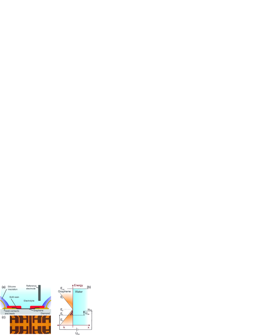
CVD graphene was grown on copper foil at in a CH4/H2/Ar atmosphere, as reported previously.Li et al. (2009) Following growth, standard methods for selective Cu etching and material transferMattevi, Kim, and Chhowalla (2011) were used to place graphene onto insulating oxygen-terminated single-crystalline diamond, which was pre-patterned with Ti/Au metal contacts. The active areas of the graphene transistors, with gate widths of 40 m and lengths of either 16 m or 26 m, were defined by UV-photolithography and oxygen plasma etching. Finally, the samples were annealed in vacuum at to remove residual contamination. SGFETs were also prepared from epitaxial graphene on the Si-face of SiC by thermal decomposition at under argon atmosphere.Emtsev et al. (2009) For these devices, the electrical leads were fabricated by local plasma oxidation of the graphene and evaporation of Ti/Au. For both CVD and SiC graphene devices, the metal contacts and leads were insulated from the electrolyte by a chemically stable photoresist (SU8). The partial overlap of the SU8 layer with the graphene in the transistor active area (3 m on both the drain and source region) resulted in devices with effective gate lengths of 10 m and 20 m. The experiments were performed in a 10 mM sodium phosphate-buffered electrolyte adjusted to a total ionic strength of 50 mM by adding NaCl. The transistors were biased in a two-electrode setup using a Ag/AgCl-wire as the reference electrode (see Fig. 1(a)). Drain-source and gate-source biases were applied using two source meters.
Fig. 2(a) shows the experimental results of the drain-source current as function of the gate voltage at a drain-source voltage of 100 mV. The current modulation shown in Fig. 2(a) results from the gate-induced shift of the Fermi level (Fig. 1(b)) which controls the density and type of charge carriers. The current minimum, which corresponds to the Dirac point , is observed at = +430 mV for CVD graphene and = -250 mV for SiC graphene. The different gate potentials of the Dirac point can be explained by substrate-induced doping. The Fermi level of ungated graphene can be estimated considering the intrinsic work function of undoped graphene ( eVYu et al. (2009)), the potential of the Ag/AgCl reference of 4.7 eV below the vacuum level, and the Dirac point. Fig. 2(a) shows that the SiC graphene is n-type doped in good agreement with previous results,Emtsev et al. (2009) with meV. On the other hand, a p-type doping, with meV, is obtained for the CVD-grown graphene. A similar position has been observed for SiO2 and is attributed to the doping effect of a water layer underneath the graphene.Wehling, Lichtenstein, and Katsnelson (2008)
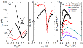
For both the electron () and the hole regime (), a deviation from a linear dependence can be observed for mV. However, the observed behavior is not symmetric for electrons and holes. For SGFET devices on CVD graphene, the slope of the curve is clearly higher for , whereas on SiC graphene devices the opposite effect is observed. Fig. 2(b) shows the transconductance of the CVD graphene SGFET in Fig. 2(a), calculated as the derivative of with respect to . This parameter is of special interest for sensor applications as it specifies the response of the transistor, i.e. the current response to a small modulation of the gate voltage, and thus its sensitivity. Maxima of are observed in both the electron and hole regimes, reaching values of 250 S (electrons) and 420 S (holes) for CVD graphene, and 110 S (electrons) and 80 S (holes) for SiC graphene.
The flattening of the current response to gate voltage observed away from the Dirac point is a consequence of the access regions. As shown in Fig. 1(a), the graphene conductivity in the region covered with SU8 cannot be controlled by the electrolytic gate. These regions will be referred to as access regions, and can be modeled by a gate independent access resistance , which is extracted by comparing transistors with different effective channel lengths but identical access regions. By removing from the total resistance of the device, the ”internal” conductivity of the transistor can be calculated (solid lines in Fig. 2(a)). The reduced current response is still present in the CVD G-SGFET for , and in the SiC G-SGFET for , suggesting a difference in electron and hole transport for both types of devices. This asymmetry can be explained by considering the contribution of the fixed Fermi level in the graphene below the SU8. Depending on the carrier type in the open channel, a p-n junction can form at the boundary with the access region, resulting in an additional resistance due to restricted carrier injection.
Based on the discussion of the substrate-induced doping, the ungated regions of the graphene transistors under the SU8 layer are expected to be p-type and n-type doped for the CVD and SiC graphene, respectively. Therefore, in the case of CVD graphene, a restriction of the electron conduction is expected when the graphene channel is biased in the n-type regime ().
For SiC graphene, on the other hand, the access regions are expected to be n-type, leading to the observed restricted hole conduction for . A similar asymmetry in the conductivity was previously observed and attributed to the doping effect of metal contacts on the underlying graphene.Huard et al. (2008) In our case, however, the local doping effect is expected to be mostly caused by the access regions.

The high transconductance of graphene SGFETs, calculated from the data in Fig. 2(a), can be explained by the combined effects of two notable properties of graphene. The interfacial capacitance of the graphene/water system has been reported to be as high as several Fcm-2.Dankerl et al. (2010) In addition, the charge carrier mobilities observed in graphene are very high, even for large-scale graphene sheets.Li et al. (2009) Both the interfacial capacitance and the mobility enter linearly into the transistor transconductance.
For the interfacial capacitance of the graphene/water interface, the contributions of the quantum capacitance of graphene and the double layer capacitance have to be considered. Recently, we have modeled the graphene/water interface using an extended Poisson-Boltzmann (ePB) model which considers the microscopic structure of interfacial water.Dankerl et al. (2010)
Fig. 3(a) shows how the total interfacial capacitance derived from the ePB model can be described by the series combination of and a of about 3 F/cm2. Using this model for the interfacial capacitance, the field effect mobility of charge carriers in the device can be obtained after correction for the access resistance.
Fig. 3(b) shows calculated from the curves of the graphene SGFETs in Fig. 2(a).
For the CVD G-SGFETs, hole mobilities greater than 1700 cm2/Vs are observed at the point of maximum transconductance. In the n-type region, however, the calculated mobilities are significantly lower. For the case of epitaxial graphene on SiC, electron mobilities are larger than hole mobilities. The lower carrier mobilities for the SiC G-SGFETs compared to the CVD G-SGFETs is consistent with previous publicationsEmtsev et al. (2009); Li et al. (2009), and is attributed to the strong electronic coupling between graphene and the underlying SiC.
Fig. 3(b) reveals that carriers in the open channel with an opposite charge to those in the access regions show a lower mobility. That is, in the presence of the p-n junctions induced by the access regions, is reduced for both CVD and SiC graphene, suggesting that the calculated for carriers in the low mobility regimes (electrons in CVD graphene, holes in SiC graphene) may require correction by considering the effect of the p-n junction.
We further compare the graphene transistors to SGFETs based on silicon, diamond, and AlGaN/GaN heterostructures. The nitride-based devices were fabricated from GaN/AlGaN/GaN heterostructures.Steinhoff et al. (2005) Diamond SGFETs were prepared using the surface conductivity of hydrogenated single crystalline diamond.Garrido et al. (2005)
Fig. 2(c) shows a comparison of the normalized transconductance for all the studied SGFETs. The maximum transconductance of the CVD graphene devices is about 20 times higher than for silicon. The superior performance of G-SGFETs can be explained by the combined effect of the mobility and the interfacial capacitance, as summarized in Table 1. AlGaN/GaN transistors, with mobilities similar to graphene, have a significantly lower interfacial capacitance due to the dielectric between the 2D electron gas and the electrolyte.Steinhoff et al. (2005) The interfacial capacitance of the diamond devices is comparable to the graphene transistors, however, the observed hole mobilities are considerably lower. In the case of silicon SGFETs,Sprössler et al. (1999) the relatively low values of capacitance and mobility result in the lowest transconductance.
| Material | (cm2/Vs) | (F/cm2) | (mS/V) |
|---|---|---|---|
| Silicon | 450 | 0.35 | 0.20 |
| Diamond | 120 | 2 | 0.29 |
| AlGaN/GaN | 1240 | 0.32 | 0.51 |
| SiC-Graphene | 400 | 2 | 1.14 |
| CVD-Graphene | 1700 | 2 | 4.23 |
In summary, solution-gated field effect transistors have been fabricated from large-scale graphene grown by CVD and by thermal decomposition of SiC. The transconductive sensitivity of the CVD graphene SGFETs is found to exceed 4 mS/V, almost one order of magnitude higher than for SGFETs based on other material systems, and results from the high interfacial capacitance and the large carrier mobilities in graphene. Recent progress in the growth of graphene with high carrier mobilities, together with improved device design which minimizes the access resistance, is expected to further increase the substantial advantages of graphene for sensing applications.
We thank A. Offenhäusser for the Si-based SGFETs and J. Howgate for the GaN-based SGFETS. This work is funded by the German Research Foundation (DFG) in the framework of the Priority Program 1459 ”Graphene”, the Bavarian Graduate School CompInt, the TUM Institute for Advanced Study (TUM-IAS), and the Nanosystems Initiative Munich (NIM).
References
- Tang et al. (2009) \BibitemOpen\bibfieldauthor L. Tang, Y. Wang, Y. Li, H. Feng, J. Lu, and J. Li, \bibfieldjournal Adv. Funct. Mater. 19, 2782 (2009)\BibitemShutNoStop
- Lu et al. (2009) \BibitemOpen\bibfieldauthor C.-H. Lu, H.-H. Yang, C.-L. Zhu, X. Chen, and G.-N. Chen, \bibfieldjournal Angewandte Chemie 121, 4879 (2009)\BibitemShutNoStop
- Ang et al. (2008) \BibitemOpen\bibfieldauthor P. K. Ang, W. Chen, A. T. S. Wee, and K. P. Loh, \bibfieldjournal J. Am. Chem. Soc. 130, 14392 (2008)\BibitemShutNoStop
- Cohen-Karni et al. (2010) \BibitemOpen\bibfieldauthor T. Cohen-Karni, Q. Qing, Q. Li, Y. Fang, and C. M. Lieber, \bibfieldjournal Nano Lett. 10, 1098 (2010)\BibitemShutNoStop
- Heller et al. (2010) \BibitemOpen\bibfieldauthor I. Heller, S. Chatoor, J. Männik, M. A. G. Zevenbergen, C. Dekker, and S. G. Lemay, \bibfieldjournal J. Am. Chem. Soc. 132, 17149 (2010)\BibitemShutNoStop
- Dankerl et al. (2010) \BibitemOpen\bibfieldauthor M. Dankerl, M. V. Hauf, A. Lippert, L. H. Hess, S. Birner, I. D. Sharp, A. Mahmood, P. Mallet, J.-Y. Veuillen, M. Stutzmann, and J. A. Garrido, \bibfieldjournal Adv. Funct. Mater. 20, 3117 (2010)\BibitemShutNoStop
- Ristein et al. (2010) \BibitemOpen\bibfieldauthor J. Ristein, W. Zhang, F. Speck, M. Ostler, L. Ley, and T. Seyller, \bibfieldjournal J. Phys. D: Appl. Phys. 43, 345303 (2010)\BibitemShutNoStop
- Berger et al. (2006) \BibitemOpen\bibfieldauthor C. Berger, Z. Song, X. Li, X. Wu, N. Brown, C. Naud, D. Mayou, T. Li, J. Hass, A. N. Marchenkov, E. H. Conrad, P. N. First, and W. A. de Heer, \bibfieldjournal Science 312, 1191 (2006)\BibitemShutNoStop
- Li et al. (2009) \BibitemOpen\bibfieldauthor X. Li, W. Cai, J. An, S. Kim, J. Nah, D. Yang, R. Piner, A. Velamakanni, I. Jung, E. Tutuc, S. K. Banerjee, L. Colombo, and R. S. Ruoff, \bibfieldjournal Science 324, 1312 (2009)\BibitemShutNoStop
- Mattevi, Kim, and Chhowalla (2011) \BibitemOpen\bibfieldauthor C. Mattevi, H. Kim, and M. Chhowalla, J. Mater. Chem. 21, 3324 (2011)\BibitemShutNoStop
- Emtsev et al. (2009) \BibitemOpen\bibfieldauthor K. V. Emtsev, A. Bostwick, K. Horn, J. Jobst, G. L. Kellogg, L. Ley, J. L. McChesney, T. Ohta, S. A. Reshanov, J. Rohrl, E. Rotenberg, A. K. Schmid, D. Waldmann, H. B. Weber, and T. Seyller, \bibfieldjournal Nat. Mater. 8, 203 (2009)\BibitemShutNoStop
- Yu et al. (2009) \BibitemOpen\bibfieldauthor Y.-J. Yu, Y. Zhao, S. Ryu, L. E. Brus, K. S. Kim, and P. Kim, \bibfieldjournal Nano Lett. 9, 3430 (2009)\BibitemShutNoStop
- Wehling, Lichtenstein, and Katsnelson (2008) \BibitemOpen\bibfieldauthor T. O. Wehling, A. I. Lichtenstein, and M. I. Katsnelson, \bibfieldjournal Appl. Phys. Lett. 93, 202110 (2008)\BibitemShutNoStop
- Huard et al. (2008) \BibitemOpen\bibfieldauthor B. Huard, N. Stander, J. A. Sulpizio, and D. Goldhaber-Gordon, \bibfieldjournal Phys. Rev. B 78, 121402 (2008)\BibitemShutNoStop
- Steinhoff et al. (2005) \BibitemOpen\bibfieldauthor G. Steinhoff, B. Baur, G. Wrobel, S. Ingebrandt, A. Offenhäusser, A. Dadgar, A. Krost, M. Stutzmann, and M. Eickhoff, \bibfieldjournal Appl. Phys. Lett. 86, 033901 (2005)\BibitemShutNoStop
- Garrido et al. (2005) \BibitemOpen\bibfieldauthor J. A. Garrido, A. Härtl, S. Kuch, M. Stutzmann, O. A. Williams, and R. B. Jackmann, \bibfieldjournal Appl. Phys. Lett. 86, 073504 (2005)\BibitemShutNoStop
- Sprössler et al. (1999) \BibitemOpen\bibfieldauthor C. Sprössler, M. Denyer, S. Britland, W. Knoll, and A. Offenhäusser, \bibfieldjournal Phys. Rev. E 60, 2171 (1999)\BibitemShutNoStop