Evidence for semiconducting behavior with a narrow band gap of Bernal graphite
Abstract
We have studied the resistance of a large number of highly oriented graphite samples with areas ranging from several mm2 to a few m2 and thickness from nm to several tens of micrometers. The measured resistance can be explained by the parallel contribution of semiconducting graphene layers with low carrier density cm-2 and the one from metalliclike internal interfaces. The results indicate that ideal graphite with Bernal stacking structure is a semiconductor with a narrow band gap meV.
pacs:
73.90.+f,61.80.-x,81.05.Uwe-mail: esquin@physik.uni-leipzig.de
1 Introduction
The study of the transport properties of graphite has been object of discussion for more that 60 years[1, 2, 3, 4, 5, 6]. The work of Slonczewski and Weiss [4] as well as that of McClure [5, 6] - both a continuation of the work of Wallace [1] on the band structure of graphene - introduced several (free) coupling parameters within a tight binding calculation and the k.p. method to obtain the graphite band structure. The parameters were then fixed using as reference transport results obtained in bulk graphite samples with carrier density per graphene layer cm-2. The apparent existence of a relatively large carrier density seemed to be compatible with the relatively small and metalliclike resistivity measured in several bulk graphite samples [7]. All these early results obtained for the graphite structure were resumed later within the so-called two-bands model for graphite developed by Kelly [7]. After that, many band structures calculations using the local density as well as others approximations [8] reached the same conclusions and claimed to fit well the experimental results, see e.g. Refs. [9, 10]. Note, however, that all these calculations depend on parameters that are being fixed to fit experimental data. If those experimental results do not reflect the intrinsic properties of ideal graphite, clearly those calculations as well as the obtained parameters cannot be taken as intrinsic of the graphite structure.
A different approach to obtain the binding energy between the planes of graphite has been proposed using Lennard-Jones potential and assuming that the binding between graphene layers is due to van der Waals forces [11, 12, 13]. These forces represent a very weak interaction and therefore it is rather clear that this approach will not give a similar band structure for graphite as the one proposed with large coupling between the graphene planes. From the experimental point of view we may now doubt that the large amount of the reported data, e.g. , do reflect ideal graphite. The exhaustive experience accumulated in gapless or narrow gap semiconductors [14] indicates already that care should be taken with the measured carrier density because it can easily be influenced by impurities and/or defects in the graphite/graphene lattice[15, 16].
We believe that the multigrain morphology of real oriented graphite samples has not been taken into account appropriately in the literature, especially its influence to the carrier density and other transport phenomena. For example, electron back scattering diffraction (EBSD) reveals typical size of the grains of a few microns in the plane within HOPG samples, see Ref. [17], a size that limits the carrier mean free path at low temperatures [18]. Moreover, the contribution to the transport properties of internal two-dimensional interfaces found recently between single crystalline regions inside the HOPG samples [19] was apparently never taken into account in the existence literature of graphite. Why these interfaces can be of extreme importance in graphite? As the results from various semiconductors show (e.g. n-Ge bicrystals [20, 21], p-InSb [22] as well as in Hg1-xCdxTe grain boundaries [23]) internal interfaces lead to the formation of confined quasi-two dimensional carrier systems with cm-2 and clear signs for the Quantum Hall effect[21]. Recently done studies demonstrated the large sensitivity of the resistivity of graphite samples to the internal interfaces that exist between crystalline regions of nm thickness, a few microns long and running mostly parallel to the graphene planes[19]. These results indicate that the earlier reported values of as well as the metalliclike behavior of the resistivity are not intrinsic of the graphite Bernal structure but are due to a large extent to the contribution of internal interfaces and defects.
The aim of this work is to propose a simple model to explain the experimental longitudinal resistance data obtained in different oriented graphite samples of different thickness and areas. The rather complicated behavior of the longitudinal resistivity can be explained assuming the parallel contribution of regions with semiconducting graphene layers and the ones from the interfaces between them, as transmission electron microscopy studies revealed[19].
2 Sample characteristics
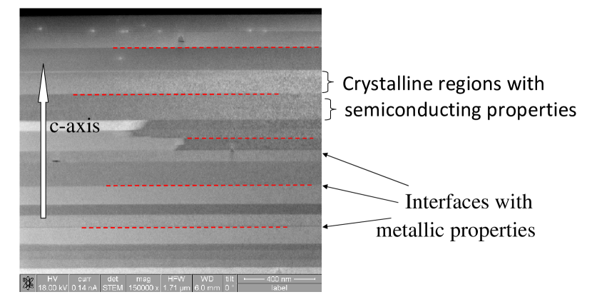
All the graphite samples were taken from the same Bernal-type highly oriented pyrolytic graphite (HOPG) sample from Advanced Ceramic of high purity (see, e.g., Ref. [24]) and with a rocking curve width of . As shown by Bernal[25], this structure has the usual ABABABA stacking of the single graphene layers inside graphite. This is the stable graphite structure, which is obtained by suitable annealing treatments eliminating also possible rhombohedral modification that results from deformation of the original hexagonal structure. The internal structure of the used samples is shown in a transmission electron microscope picture in Fig. 1. As shown in Ref. [19] this picture reveals single crystalline regions of graphene layers of thickness between 30 nm and nm. These regions are clearly recognized in Fig. 1 through the different gray scales and have sightly different orientation between each other, e.g. different angle misalignments. We note that a rotation up to 30 degrees between the graphene layers from neighboring graphite regions has been seen by HRTEM in few layers graphene sheets in Ref. [26].
Important to understand the measured behavior of the resistance of graphite samples is the existence of well defined interfaces between the single crystalline regions. As we mentioned in the introduction, interfaces between crystalline regions in semiconductors with different orientations for example [20, 21, 22, 23], lead to confined quasi-two dimensional carrier systems with much larger carrier density than the bulk matrix. We assume therefore that these interfaces running parallel to the graphene layers of the graphite structure are the origin of the metallic like resistivity as well as for the apparent large carrier density measured in bulk samples, i.e. cm-2, an assumption that is supported by the change of the absolute resistivity with thickness [19].
Taking into account the internal microstructure of the graphite samples it is clear that it is necessary to measure the resistance of samples of small enough thickness in order to get the intrinsic transport of the graphite structure with its weak coupled graphene layers. The micrometer small samples and with thickness below 100 nm were prepared by a rubbing method[19]. The resistivity data were obtained with four contacts and checking the ohmic behavior at room temperature. The deposited Pd/Au contacts on the micrometer large graphite flakes were prepared by electron lithography and micro-Raman characterization was used to check for the sample quality[19], as the inset in Fig. 2 demonstrates. Following the characterization work of Ref. [27], the Raman spectra confirm the similar stacking between the bulk and thin graphite samples. Micrometer large mean free path at 300 K and low carrier density[28, 29] are a further proof of the high quality of the thin graphite flakes discussed in this work.
3 Temperature dependence of the carrier density
We start with the temperature dependence of the carrier density obtained from a 40 nm thin and several micrometers large graphite flake sample. It is important to recognize that due to the large mean free path of the carriers in the graphene layers within the graphite structure, ballistic not diffusive transport has to be taken into account[18, 29]. To obtain the mean free path or the intrinsic carrier density of the graphene layers inside graphite one cannot use straightforwardly the Boltzmann-Drude approach to interpret the longitudinal and transverse resistances. Due to the large mean free path of the carriers in the weakly coupled graphene layers within the graphite structure it is possible to use experimental methods where the ballistic transport is clearly revealed. One possible experimental method is the constriction method based on the measurement of the longitudinal resistance as a function of the width of a constriction located between the voltage electrodes. When the ballistic contribution overwhelms the diffusive ones and allows us to obtain and without the need of free parameters or arbitrary assumptions[18, 28]. Other experimental method is the measurement of the length dependence of the resistance. If ballistic transport is important then a finite resistance is extrapolated at zero sample length, a value that can be used to obtain directly the mean free path without free parameters or arbitrary assumptions [29]. Both independent methods provide similar large carrier mean free path as well as much lower carrier density as those found in the literature for bulk graphite samples.
Figure 2 shows for a thin graphite sample; it follows an exponential dependence with an activation energy or energy gap meV. Due to the small gap and from Fig. 2 it is not obvious that the experimental curve follows an exponential behavior and not a linear one at temperatures above the saturation region. A simple way to distinguish that, it is calculating the temperature derivative. In case of a linear temperature behavior we expect a saturating upper derivative value at high temperatures but a shallow maximum for the exponential function at intermediate temperatures. The bottom right inset shows the calculated derivative for both curves, the experimental and the exponential function fit. It is clear that the exponential function provides the correct temperature dependence of the carrier density. The shallow minimum in (main panel in Fig. 2) at K is an artifact due to interfaces, at least that one between the substrate and sample and/or the sample free surface. The finite value of can be due to this interface contribution or due to lattice defects[15] including a very small amount of impurities like hydrogen; note that cm-2 would mean of the order of a single hydrogen atom or C-vacancy in m2 graphene area.
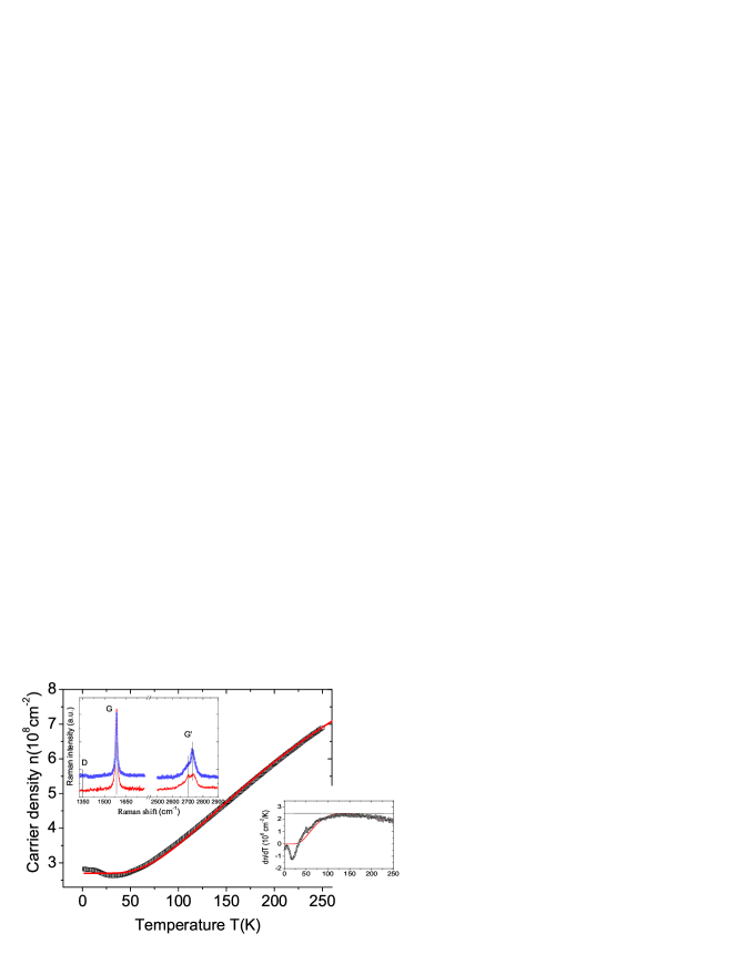
One may be surprised to get such low carrier density in comparison with usual values reported in the literature for graphite, e.g. cm-2 [7, 9, 10]. We note first that the measured graphite sample has a thickness less than 50 nm and therefore much less contribution of interfaces. Second, the measured carrier density of graphite reported in literature was obtained mostly for bulk samples with an unknown concentration of interfaces as well as defects. Further independent evidence that supports an intrinsic low carrier density in graphite is given by the vanishing of the Shubnikov-de Haas (SdH) oscillations in the magnetoresistance the thinner the graphite sample, an experimental fact already reported in 2001 that to our knowledge remained without explanation [30]. Note that older publications reported SdH oscillations of very large amplitude, e.g. Ref. [31], in comparison with the rather weak amplitudes, if at all observed, found nowadays in better quality samples or thin enough graphite samples. A clear demonstration that these SdH oscillations are actually non-intrinsic of ideal graphite is given by their appearance in thin graphite samples after introducing defects by irradiation as shown in Refs. [15, 32].
4 Temperature dependence of the resistance of different graphite samples
Following the results from Ref. [19] as well as the semiconducting behavior of , see Fig.2, obtained for a thin graphite sample, we assume therefore that the graphene layers inside each graphite sample are semiconducting and altogether and between the voltage electrodes their signal depends on an effective resistance of the type:
| (1) |
The prefactor depends basically on the mobility, i.e. the mean free path and on details of the carriers band structure (e.g. effective mass). If we take into account in the temperature dependence of the mean free path recently obtained for similar samples, i.e. ( in m and in K), see Ref. [29], the absolute value of the energy gap obtained from the fits to the data remains the same within the confidence limits of 35%. For simplicity we will take as a temperature independent parameter as well as the energy gap . The absolute value of the prefactor (as well as of the other prefactors) will change from sample to sample; note that we estimate the resistance of a given sample not its resistivity.
For samples with thickness larger than nm and of several micrometers length there is a larger probability to have interfaces, which signals will be picked up by the voltage contact electrodes (usually several micrometers apart). Therefore, in parallel to we simulate the contribution from the interfaces through the resistance:
| (2) |
where the coefficients as well as the activation energy are free parameters. The temperature independent term in Eq. (2) represents the residual resistance measurable at low enough temperatures. The unusual thermally activated term as well as the, in general weak, linear one will be discussed at the end. The total resistance is given by the parallel contribution of and as . Clearly, by changing the parameters one can obtain all types of behavior for . We will see that a consistent description of the data can be indeed reached and that the main free parameter is similar for all samples.
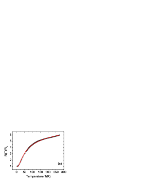
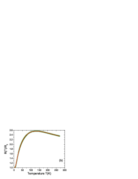
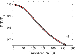
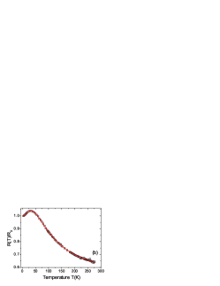
Figures 3 and 4 show the normalized resistance vs. temperature and the fits with the parallel resistance model described above of six different samples with different weights between the intrinsic semiconducting and the non-intrinsic interface contribution. That is why the pre-factors of the main terms in must change from sample to sample, i.e. and , because we do not fit the resistivity but the resistance. From all the obtained data and within the confidence limits of the fitting we obtain an energy gap meV, independently of the sample geometry, i.e. a similar energy gap is obtained for very thin as well as thick graphite samples if the contribution of the interfaces does not short circuit completely that from the graphite crystalline regions. This fact indicates that we are not dealing here with a special graphite structure found only in a few tens of nanometers thick samples. This is the main result of this study.
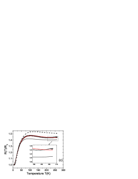
We stress that the interfaces as well as the single crystalline regions are restricted in thickness as well as in the plane parallel to the graphene layers. This fact supports the use of the simple parallel resistance model. For thick enough graphite samples (thickness m) the contribution of the interfaces overwhelms and the measured resistance will be mainly given by Eq. (2), as the results for bulk HOPG sample shows, see Fig. 3(a). The exponential term with an activation energy K is of the same order as reported in Ref. [33] for similar samples. To fit the data shown in Fig. 3(a) a relatively small linear-temperature term contributes at high temperatures.
, ,
,
,
 ,
, 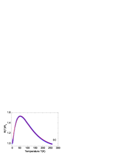
In general the semiconducting behavior starts to be clearly visible in thinner samples due to the decrease in the amount of interfaces; obviously there is no sharp thickness threshold because the properties of the interfaces as well as the defects and carrier concentrations vary from sample to sample, affecting the relative weight between the two parallel contributions. The results shown in Figs. 3(b) and (c) are examples where the two contributions and compete. For samples thinner than nm the semiconducting behavior starts to overwhelm that from the interfaces, see Fig. 4.
Note that this semiconducting behavior is observed for a range of about five orders of magnitude in sample area and that the width or length of the samples overwhelms the intrinsic Fermi wavelength of the graphene planes inside the sample[28] m. Therefore, the semiconducting behavior is not due to a quantum confinement shift, as observed in Bi nanowires[34] of small diameter . We stress that our results should not be interpreted as a metallic to semiconducting transition as a function of thickness, but only the weight between the two parallel contributions changes upon sample thickness. Because at least the interfaces sample-substrate and sample-surface remain, as for the sample of Fig. 4(a), both parallel contributions are always present. We note that the dependence of the axis resistivity of graphite with pressure [35] shows similar characteristics as the ones for the resistivity in plane shown here. The axis resistivity behavior was basically interpreted with a tunnel barrier for the electrons between planes and crystallites.
5 Discussion
We would like to discuss the question of the existence of an energy gap taking into account results from literature and whether this intrinsic semiconducting behavior has been observed in the past. (a) As we discussed above and taking into account the contribution of the interfaces bulk graphite samples have, it is clear that the behavior obtained in transport measurements of those samples is not intrinsic. Therefore we cannot consider those experimental results as a proof for the apparent metallicity of graphite.
(b) One would expect that infrared (IR) measurements show somehow the semiconducting behavior. However, those measurements, as for example in Ref. [36], were done in bulk samples (several mm2 area and several hundreds of micrometers thick) that show clear SdH oscillations [37] with the usual carrier density above cm-2 per graphene layer and therefore do not represent intrinsic graphite. Note that the internal interfaces, see Fig. 1, and due to their large carrier density in comparison with the crystalline regions, are those regions that provide a shielding to the electromagnetic wave used in IR measurements. In general we remark that spectroscopy methods are not completely reliable when one wants to resolve a gap of 40 meV in samples that are inhomogeneous for the reasons discussed above. Therefore, we believe that the intrinsic properties of the single crystalline graphite regions are not actually seen by this technique. Also other experimental techniques, see e.g. Ref. [38], would have problems to recognize an electronic band structure with an energy gap of the order of 40 meV if the carrier density is much larger than the intrinsic one of ideal, defect free graphite.
(c) We may ask about the results on graphite using angle-resolved photoemission spectroscopy (ARPES) published several times in the past. There are three points we should take into account about ARPES results. Firstly, this technique is surface sensitive, although we may expect to see to some extent a vestige of the bulk band edge. Second, different samples may provide different results. A clear correlation between sample quality and other of its characteristics with the ARPES results is difficult because one not not always find the necessary information in the reported studies. Finally the scanned sample area and the energy resolution of the usual spectroscopy systems. We know from other techniques like electron back scattering diffraction (EBSD) [17] or electron force microscopy (EFM) [39] that homogeneous regions of graphite appear to be in the region of m (parallel to the planes) or smaller. Regarding the energy resolution we find, for example, in the ARPES work of Ref. [40] a resolution of 15 meV to 65 meV, in Ref. [41] it is from 15 meV to 40 meV and in Ref. [42] 40 meV. This resolution appears to be too low to clearly resolve an energy gap of the order of 30 to 50 meV in bulk graphite. A better energy resolution between 4 to 15 meV has been achieved in Refs. [43, 9] using kish and natural graphite samples, respectively. Interestingly, in Ref. [43] an energy gap of 25 meV between the and bands at the K(H) point was reported whereas in Ref. [9] an energy gap of meV has been inferred from the band fits near the H point, although the used sample had apparently an average carrier density of cm-2 (at 25 K). Clearly, higher energy resolution, smaller scanned areas and clearer sample quality aspects are necessary in future experiments using this technique.
(d) In general we note that techniques that are sensitive to the surface do not necessarily provide the intrinsic properties of graphite. Apart from the extra doping graphite surfaces may have due to defects and added atoms or molecules, we note that the surface itself may have a different electronic structure as the graphene layers inside the Bernal structure due to the total absence of coupling with a graphene layer above it. Therefore, STM experiments on the graphite surface do not necessarily provide the intrinsic behavior of graphite with certainty. However, there are STM experiments that suggest the existence of an energy gap of the same magnitude as the one obtained in this work. This energy gap appeared in a few graphene layers[44] from ”unidentified states” or levels that at zero magnetic field do not coalesce, a result supported by Hubbard calculations with a constant potential[45]. Clearly, if a few graphene layers shows an energy gap, there seems to be no simple reason to rule out that graphite should not have it. Note also that in Ref. [44] other electronic contributions, partially due to Dirac fermions, have been obtained at the surface. This fact suggests that the resistance of this interface (or between the sample and substrate) will provide a different conduction path in parallel to the semiconducting one from the internal graphene layers. This gives a simple explanation for the saturation in resistance measured at low temperatures.
(e) In order to compare the results of the temperature dependence of the resistance obtained in single or a few layers graphene samples with our results one should compare the one obtained at the lowest carrier density possible. This has been done in, e.g., Ref. [46] where one recognizes that at the lowest carrier density reached near the neutrality point (former Dirac point) the resistance does not behave metallic but rather semiconducting. Increasing the carrier density only slightly with the bias voltage, the resistance starts to show signs of metallicity[46] . Further semiconducting behavior in has been seen in Refs. [47] and [48].
(f) And at last but not least we would like to point out the recently done optical pump-probe spectroscopy experiments on 30 nm thick graphite flake [49], a sample geometry relevant for comparison with our study. Even for excitation densities 10 times larger than the one of our samples, these experiments suggest a renormalization of the band gap by meV, which is nearly constant during the first picosecond. The authors in Ref. [49] conclude that carrier equilibration in graphite is similar to semiconductors with a nonzero band gap.
The interaction between graphene planes in graphite is van der Waals type, which gives a binding energy of K. That means that each graphene layer should be very little affected and therefore the electron electron interaction may be also active in graphite as also in ideal single graphene as well. This cannot be excluded because the data obtained in the literature are for large and therefore any gap of the magnitude we obtain here will not be so easily measurable. Electron interactions are large and for a small enough carrier density the expected screening will be very weak promoting therefore the existence of an energy gap. This is what it is observed in Monte Carlo simulations for the unscreened Coulomb interaction in graphene with different Dirac flavors[50].
Before concluding we would like to discuss the possible origin of the exponential function in Eq. (2) because this is not the usual one expects for metals or semimetals and cannot be understood within the usual electron-phonon interaction mechanisms also in two dimensions. We note that this function has been already used to describe the increasing resistance of bulk graphite samples with temperature and speculated to be related to some superconducting-like behavior in graphite[33]. We note further that a similar dependence has been observed in granular Al-Ge[51], which shows for a particular Al concentration a semiconductor-superconductor transition practically identical to that in Fig. 4(c). The thermally activated behavior in Eq. (2) can be understood on the basis of the Langer-Ambegaokar-McCumber-Halperin (LAMH) model[52, 53] that applies to narrow superconducting channels in which thermal fluctuations can cause phase slips. The value of the activation energy obtained from the fits depends on the measured sample and it is between 10 K and 40 K for a large amount of measured samples.
Although we do not claim that this exponential function is due to granular superconductivity embedded within the interfaces shown in Fig. 1, this speculation matches however a series of experimental hints obtained recently. We would like to mention that the possible existence of high-temperature superconductivity in non-percolative regions within the internal interfaces found in highly oriented pyrolytic graphite has been proposed recently [19] . The experimental hints are quite diverse and all of them point in the same direction: (1) Huge magnetic field driven metal-insulator transition in bulk graphite [54, 55]. This transition vanishes for thin enough samples because of the lack of the internal interfaces. (2) Superconducting-like hysteresis loops in the magnetization of pure HOPG samples [56, 57]. (3) Anomalous hysteresis in the magnetoresistance of mesoscopic graphite samples, similar to those found in granular superconductors [58, 59]. (4) Quantum oscillations in the magnetoresistance in multigraphene samples based on Andreev-scattering mechanism [58]. (5) Superconducting-like magnetic field driven transition in the resistance of an internal interface of a graphite flake [60]. (6) Finally, Josephson-like characteristic curves found in thin graphite lamellas [61].
Since most of the theoretical predictions emphasize that superconductivity should be possible under the premise that the carrier density per graphene area cm-2 in order to reach K, it is then appealing that regions at the internal interfaces within the graphite structure may have superconducting patches due to its much higher carrier density. We note that interfaces in some semimetals materials like Bi can be superconducting [62, 63].
The weak linear term in Eq. (2) provides a typical metallic dependence to the resistance, which may come from the metallic regions within the interfaces. This small term is not always necessary to get a reasonable fit to the data and can be even negative (or may follow a weak variable range hopping dependence) as appears to be the case for the sample-substrate and/or sample-surface interfaces, see Fig. 4(a). Even in the case of total absence of internal interfaces, as for example for thin enough samples, it is clear that the semiconducting behavior of the intrinsic graphite regions cannot be observed at low enough temperatures due to the parallel contributions of the surface and/or substrate/sample.
Concluding, the temperature dependence of the electrical resistance of oriented graphite samples can be quantitatively understood assuming the parallel contribution of semiconducting and normal metallic (and/or granular superconducting) regions. The semiconducting contribution clearly indicates that Bernal graphite is a semiconductor with a narrow gap of the order of 40 meV. We speculate that the existence of narrow band gap we observe in graphite may be applicable to other semimetals. In other words we doubt on the existence of strictly zero band gap in nature.
This work is supported by the Deutsche Forschungsgemeinschaft under contract DFG ES 86/16-1. S.D. is supported by the Graduate School of Natural Sciences “BuildMoNa” of the University of Leipzig.
References
- [1] P. R. Wallace. The band theory of graphite. Phys. Rev, 71:622, 1947. see also the Erratum in Phys. Rev. 72, 258 (1947),.
- [2] R. R. Haering and P. R. Wallace. The electric and magnetic properties of graphite. J. Phys. Chem. Solids, 3:253–274, 1957.
- [3] R. R. Haering and S. Mrozowski. Progress in Semiconductors, volume V. Heywood and Company Ltd., London, 1960.
- [4] J. C. Slonczewski and P. R. Weiss. Band structure of graphite. Physical Review, 109:272, 1958.
- [5] J. W. McClure. Band structure of graphite and de Haas-van Alphen effect. Physical Review, 108:612, 1957.
- [6] J. W. McClure. Analysis of multicarrier galvanomagnetic data for graphite. Physical Review, 112:715, 1958.
- [7] B. T. Kelly. Physics of Graphite. London: Applied Science Publishers, 1981.
- [8] M. C. Schabel and J. L. Martins. Energetics of interplanar binding in graphite. Phys. Rev. B, 46:7185–7188, 1992.
- [9] A. Grüneis, C. Attaccalite, T. Pichler, V. Zabolotnyy, H. Shiozawa, S. L. Molodtsov, D. Inosov, A. Koitzsch, M. Knupfer, J. Schiessling, R. Follath, R. Weber, P. Rudolf, R. Wirtz, and A. Rubio. Electron-electron correlation in graphite: A combined angle-resolved photoemission and first-principles study. Phys. Rev. Lett., 100:037601, 2008.
- [10] J. M. Schneider, M. Orlita, M. Potemski, and D. K. Maude. Consistent interpretation of the low-temperature magnetotransport in graphite using the Slonczewski-Weiss-McClure 3d band-structure calculations. Phys. Rev. Lett., 102:166403, 2009.
- [11] L. A. Girifalco, Miroslav Hodak, and Roland S. Lee. Carbon nanotubes, buckyballs, ropes, and a universal graphitic potential. Phys. Rev. B, 62:13104–13110, 2000.
- [12] L. A. Girifalco and R. A. Lad. Energy of cohesion, compressibility, and the potential energy functions of the graphitic system. The Journal of Chemical Physics, 25:693, 1956.
- [13] N. García. unpublished, 2011.
- [14] I. M. Tsidilkovski. Electron Spectrum of Gapless Semiconductors, volume 116 of Springer Series in Solid-State Sciences. Springer Verlag, 1997.
- [15] A. Arndt, D. Spoddig, P. Esquinazi, J. Barzola-Quiquia, S. Dusari, and T. Butz. Electric carrier concentration in graphite: Dependence of electrical resistivity and magnetoresistance on defect concentration. Phys. Rev. B, 80:195402, 2009.
- [16] T. Stauber, N. M. R. Peres, and F. Guinea. Electronic transport in graphene: A semiclassical approach including midgap states. Phys. Rev. B, 76:205423, 2007.
- [17] J. C. González, M. Muñoz, N. García, J. Barzola-Quiquia, D. Spoddig, K. Schindler, and P. Esquinazi. Sample-size effects in the magnetoresistance of graphite. Phys. Rev. Lett., 99:216601, 2007.
- [18] N. García, P. Esquinazi, J. Barzola-Quiquia, B. Ming, and D. Spoddig. Transition from ohmic to ballistic transport in oriented graphite: Measurements and numerical simulations. Phys. Rev. B, 78:035413, 2008.
- [19] J. Barzola-Quiquia, J.-L. Yao, P. Rödiger, K. Schindler, and P. Esquinazi. Sample size effects on the transport properties of mesoscopic graphite samples. phys. stat. sol. (a), 205:2924–2933, 2008.
- [20] B. M. Vul and E. Y. Zavaritzkaya. Two dimensional electronic phenomena in bicrystals of germanium at He temperatures. Zh. Eksp. Teor. Fiz., 76:1089–1099, 1979.
- [21] S. Uchida, G. Landwehr, and E. Bangert. Electric subbands in p-type germanium inversion layers. Solid State Commun., 45:869–872, 1983.
- [22] R. Herrmann, W. Kraak, G. Nachtwei, and G. Worm. Shubnikov-de Haas effect of n-inversion layers in InSb grain boundaries. Solid State Commun., 52:843–845, 1984.
- [23] F. Ludwig, G. Nachtwei, M. Watts, N. J. Bassom, H.-U Müller, W. Kraak, P. Gille, and R. J. Nicholas. Cyclotron resonance of the quasi-two-dimensional electron gas at Hg1-xCdxTe grain boundaries. Semicond. Sci. Technol., 7:511–515, 1992.
- [24] H. Ohldag, P. Esquinazi, E. Arenholz, D. Spemann, M. Rothermel, A. Setzer, and T. Butz. The role of hydrogen in room-temperature ferromagnetism at graphite surfaces. New Journal of Physics, 12:123012, 2010.
- [25] J. D. Bernal. The structure of graphite. Proc. R. Soc. Lond., 106:749–773 , 1924.
- [26] J. H. Warner, M. H. R mmeli, T. Gemming, B. B chner, and G. A. D. Briggs. Direct imaging of rotational stacking faults in few layer graphene. Nano Letters, 9(1):102–106, 2009.
- [27] A. C. Ferrari, J. C. Meyer, V. Scardaci, C. Casiraghi, M. Lazzeri, F. Mauri, S. Piscanec, D. Jiang, K. S. Novoselov, S. Roth, and A. K. Geim. Raman spectrum of graphene and graphene layers. Phys. Rev. Lett., 97:187401, 2006.
- [28] S. Dusari, J. Barzola-Quiquia, P. Esquinazi, and N. García. Ballistic transport at room temperature in micrometer-size graphite flakes. Phys. Rev. B, 83:125402, 2011.
- [29] P. Esquinazi, J. Barzola-Quiquia, S. Dusari, and N. García. Length dependence of the resistance in graphite: Influence of ballistic transport. J. Appl. Phys., 111:033709, 2012.
- [30] Y. Ohashi, K. Yamamoto, and T. Kubo. Shubnikov - de Haas effect of very thin graphite crystals. 2001. Carbon’01, An International Conference on Carbon, Lexington, KY, United States, July 14-19.
- [31] D. E. Soule, J. W. McClure, and L. B. Smith. Study of the Shubnikov-de Haas effect. determination of the Fermi surfaces in graphite. Phys. Rev., 134:A453–A470, 1964.
- [32] J. Barzola-Quiquia, S. Dusari, G. Bridoux, F. Bern, A. Molle, and P. Esquinazi. The influence of Ga+ irradiation on the transport properties of mesoscopic conducting thin films. Nanotechnology, 21:145306, 2010.
- [33] Y. Kopelevich, P. Esquinazi, J. Torres, R. da Silva, H. Kempa, F. Mrowka, and R. Ocaña. Studies of High Temperature Superconductors, volume 45, chapter 3, pages 59–106. Nova Science Publishers, Inc., 2003. ISBN 1-59033-697-6.
- [34] T. E. Huber, A. Nikolaeva, L. Konopko, and M. J. Graf. Observation of three-dimensional behavior in surface states of bismuth nanowires and the evidence for bulk-bi surface quasiparticles. Phys. Rev. B, 79:201304, 2009.
- [35] C. Uher, R. L. Hockey, and E. Ben-Jacob. Pressure dependence of the c-axis resistivity of graphite. Phys. Rev. B, 35:4483–4488, 1987.
- [36] Z. Q. Li, S.-W. Tsai, W. J. Padilla, S. V. Dordevic, K. S. Burch, Y. J. Wang, and D. N. Basov. Infrared probe of the anomalous magnetotransport of highly oriented pyrolytic graphite in the extreme quantum limit. Phys. Rev. B, 74:195404, 2006.
- [37] Y. Kopelevich, P. Esquinazi, J. H. S. Torres, R. R. da Silva, and H. Kempa. volume 43 of Advances in Solid State Physics, B. Kramer (Ed.), pages 207–222. Springer-Verlag Berlin, 2003.
- [38] P. Kossacki, C. Faugeras, M. Kühne, M. Orlita, A. A. L. Nicolet, J. M. Schneider, D. M. Basko, Yu. I. Latyshev, and M. Potemski. Electronic excitations and electron-phonon coupling in bulk graphite through raman scattering in high magnetic fields. Phys. Rev. B, 84:235138, 2011.
- [39] Y. Lu, M. Muñoz, C. S. Steplecaru, Cheng Hao, Ming Bai, N. García, K. Schindler, and P. Esquinazi. Electrostatic force microscopy on oriented graphite surfaces: Coexistence of insulating and conducting behaviors. Phys. Rev. Lett., 97:076805, 2006. See also the comment by S. Sadewasser and Th. Glatzel, Phys. Rev. Lett. 98: 269701, 2007 and the reply by Lu et al., idem 98: 269702, 2007 and also R. Proksch, Appl. Phys. Lett. 89: 113121, 2006.
- [40] S. Y. Zhou, G.-H. Gweon, J. Graf, A. V. Fedorov, C. D. Spataru, R.D. Diehl, Y. Kopelevich, D.-H. Lee, S. G. Louie, and A. Lanzara. Direct observation of Dirac fermions in graphite. Nature Physics, 2:595, 2006.
- [41] S. Y. Zhou, G.-H. Gweon, and A. Lanzara. Low energy excitations in graphite: the role of dimensionality and lattice defects. Annals of Physics, 321:1730, 2006.
- [42] C. S. Leem, B. J. Kim, Chul Kim, S. R. Park, T. Ohta, A. Bostwick, E. Rotenberg, H. D. Kim, M. K. Kim, H. J. Choi, and C. Kim. Effect of linear density of states on the quasiparticle dynamics and small electron-phonon coupling in graphite. Phys. Rev. Lett., 100:016802, 2008.
- [43] K. Sugawara, T. Sato, S. Souma, T. Takahashi, and H. Suematsu. Anomalous quasiparticle lifetime and strong electron-phonon coupling in graphite. Phys. Rev. Lett., 98:036801, 2007.
- [44] G. Li and E. Y. Andrei. Observation of Landau levels of Dirac fermions in graphite. Nat. Phys., 3:623, 2007.
- [45] Z. Y. Meng, T. C. Lang, S. Wessel, F. F. Assaad, and A. Muramatsu. Quantum spin liquid emerging in two-dimensional correlated Dirac fermions. Nature, 464:847–851, 2010.
- [46] V. Skákalová, A. B. Kaiser, J. S. Yoo, D. Obergfell, and S. Roth. Correlation between resistance fluctuations and temperature dependence of conductivity in graphene. Phys. Rev. B, 80:153404, 2009.
- [47] S. V. Morozov, K. S. Novoselov, M. I. Katsnelson, F. Schedin, D. C. Elias, J. A. Jaszczak, and A. K. Geim1. Giant intrinsic carrier mobilities in graphene and its bilayer. Phys. Rev. Lett., 100:016602, 2008.
- [48] Y.-W. Tan, Y. Zhang, H.L. Stormer, and P. Kim. Temperature dependent electron transport in graphene. Eur. Phys. J. Special Topics, 148:15–18, 2007.
- [49] M. Breusing, C. Ropers, and T. Elsaesser. Ultrafast carrier dynamics in graphite. Phys. Rev. Lett., 102:086809, 2009.
- [50] J. E. Drut and T. A. Lähde. Is graphene in vacuum an insulator? Phys. Rev. Lett., 102:026802, 2009. See also Phys. Rev. B 79, 241405(R) (2009).
- [51] Y. Shapira and G. Deutscher. Semiconductor-superconductor transition in granular Al-Ge. Phys. Rev. B, 27:4463–4466, 1983.
- [52] J. S. Langer and Vinay Ambegaokar. Intrinsic resistive transition in narrow superconducting channels. Phys. Rev., 164:498–510, 1967.
- [53] D. E. McCumber and B. I. Halperin. Time scale of intrinsic resistive fluctuations in thin superconducting wires. Phys. Rev. B, 1:1054–1070, 1970.
- [54] H. Kempa, Y. Kopelevich, F. Mrowka, A. Setzer, J. H. S. Torres, R. Höhne, and P. Esquinazi. Magnetic field driven superconductor-insulator-type transition in graphite. Solid State Commun., 115:539–542, 2000.
- [55] X. Du, S.-W. Tsai, D. L. Maslov, and A. F. Hebard. Metal-insulator-like behavior in semimetallic bismuth and graphite. Phys. Rev. Lett., 94:166601, 2005.
- [56] Y. Kopelevich, P. Esquinazi, J.H.S. Torres, and S. Moehlecke. Ferromagnetic- and superconducting-like behavior of graphite. J. Low Temp. Phys., 119:691–702, 2000.
- [57] Y. Kopelevich and P. Esquinazi. Ferromagnetism and superconductivity in carbon-based systems. J. Low Temp. Phys., 146:629–639, 2007. and refs. therein.
- [58] P. Esquinazi, N. García, J. Barzola-Quiquia, P. Rödiger, K. Schindler, J.-L. Yao, and M. Ziese. Indications for intrinsic superconductivity in highly oriented pyrolytic graphite. Phys. Rev. B, 78:134516, 2008.
- [59] S. Dusari, J. Barzola-Quiquia, and P. Esquinazi. Superconducting behavior of interfaces in graphite: Transport measurements of micro-constrictions. J Supercond Nov Magn, 24:401–405, 2011.
- [60] J. Barzola-Quiquia and P. Esquinazi. Ferromagnetic- and superconducting-like behavior of the electrical resistance of an inhomogeneous graphite flake. J Supercond Nov Magn, 23:451–455, 2010.
- [61] J. Barzola-Quiquia, A. Ballestar, S. Dusari, and P. Esquinazi. Experimental Study of the Intrinsic and Extrinsic Transport Properties of Graphite and Multigraphene Samples, chapter 8 Graphene. Intech, Open Access Publisher, 2011. ISBN 978-953-307-292-0.
- [62] F.M. Muntyanua, A. Gilewski, K. Nenkov, J. Warchulska, and A. Zaleski. Experimental magnetization evidence for two superconducting phases in Bi bicrystals with large crystallite disorientation angle. Phys. Rev. B, 73:132507, 2006.
- [63] F.M. Muntyanua, A. Gilewski, K. Nenkov, A. Zaleski, and V. Chistol. Superconducting crystallite interfaces with up to 21 K in Bi and Bi-Sb bicrystals of inclination type. Solid State Commun., 147:183, 2008.