Doping effects in AlGaAs lasers with separate confinement heterostructures (SCH). Modeling optical and electrical characteristics with Sentaurus TCAD.
Abstract
Optical and electrical characteristics of AlGaAs lasers with separate confinement heterostructures are modeled by using Synopsys’s Sentaurus TCAD and open source software for semi-automatic data analysis of large collections of data. The effects of doping in all laser layers are investigated with the aim to achieve optimal characteristics of the devise. The results are compared with these obtained for real lasers produced at Polyus research institute in Moscow, showing that a significant improvement can be achieved, in particular an increase in optical efficiency (up to over 70 %) by careful control of type and level of doping through out the entire structure.
1 Introduction
An idea of Alferov et al., [1], comprising the use of a geometrically-narrow active recombination region where photon generation occurs (Quantum Wells; QW), with waveguides around improving the gain to loss ratio (separate confinement heterostructures; SCH), has largely dominated the field of optoelectronics development in the past years. AlGaAs edge emitting lasers are an example of practical realization of these ideas.
Now, they are mostly used for pumping solid state lasers used either in high-power metallurgical processes or, already, in first field experiments as a highly directional source of energy in weapons interceptors.
In our earlier works we first were able to find agreement between our calculations of quantum well energy states and the lasing wavelength observed experimentally [2]. Next [3], several changes in structure of SCH AlGaAs lasers have been shown to considerably improve their electrical and optical parameters. We compared computed properties with these of lasers produced by Polyus research institute in Moscow [5], [6].
In particular, by changing the width of active region (Quantum Well), waveguide width, as well by changing the waveguide profile by introducing a gradual change of Al concentration, we were able to decrease significantly the lasing threshold current, increase the slope of optical power versus current, and increase optical efficiency [3].
We have shown also [4] that the lasing action may not occur at certain widths or depths of Quantum Well (QW), and the threshold current as a function of the width may have discontinuities. The effects are more pronounced at low temperatures. We argue that these discontinuities occur when the most upper quantum well energy values are very close to either conduction band or valence band energy offsets. The effects may be observed at certain conditions in temperature dependence of lasing threshold current as well.
The main chalanges with the broader use of AlGaAs based SCH lasers are related to improving some of their electro-optical characteristics, in particular their optical efficiency.
The purpose of this work is to investigate the role of doping levels across the laser structure, and, if only possible, to find doping concentrations that would lead to the best opto-electrical parameters, maximizing optical efficiency.
We assume here uniform doping profiles accross laser layers.
For simulations, we use Sentaurus TCAD from Synopsys [7], which is an advanced commercial computational environment, a collection of tools for performing modeling of electronic devices.
2 Lasers structure and callibration of modeling.
We model a laser with cavity length and laser width, with doping/Al-content as described in Table 1. The table 2 describes its experimental parameters.
Synopsys’s Sentaurus TCAD, used for modeling, can be run on Windows and Linux OS. Linux, once mastered, offers more ways of an efficient solving of problems by providing a large set of open source tools and ergonomic environment for their use, making it our preferred operating system. This is an advanced, flexible set of tools used for modeling a broad range of technological and physical processes in the world of microelectronics phenomena. In case of lasers, some calculations in Sentaurus have purely phenomenological nature. The electrical and optical characteristics depend, primarily, on the following computational parameters that are available for adjusting:
of electrodes, , in Physics section, , electrical contact resistance . There are several parameters for adjustment that are related to microscopic physical properties of materials or structures studied. However, often their values are either unknown exactly or finding them would require quantum-mechanical modeling of electronic band structure and transport, based on first-principles. This is however not the aim of our work.
In order to find agreement between the calculated results and these observed experimentaly (the threshold current and the slope of Optical Power, , are such most basic laser parameters), we adjust accordingly values of and .
The results for and , in this paper, are all shown normalized by and , respectively, which are the values computed for the reference laser described in Table 1.
We neglect here the effect of contact resistance, , by not including buffer and substrate layers and contacts into calculations (compare with structure described in Table 1). We use parameter available in Sentaurus and treat it as a physical quantity that is closely related to voltage applied. Another parameter available in Sentaurus, , is simply related to by the ohmic formula: . Hence, any results shown here may be easy adjusted after calculations by adding the effect of .
Let us estimate the value of . We assume that this is the sum of electrical resistance of n-substrate, n-buffer, and p-contact layers (see Table 1). By using simplified formula for each of these layers, , and electron/hole mobility from database of Synopsys, we have the following specific resistivity values for these layers (indexed as rows in Table 1): , , and . Taking into account appropriate geometrical dimensions, we obtain: , , and . Hence, is dominated by the resistance of n-substrate layer and it is of the order of . At threshold current of , that small resistance will cause a difference between computed by us lasing offset voltage and that one measured by about only. In will however have a noticeable contribution to differential resistance .
| No | Layer | Composition | Doping [] | Thickness [] |
| 1 | n-substrate | n-GaAs (100) | 350 | |
| 2 | n-buffer | n-GaAs | 0.4 | |
| 3 | n-emitter | 1.6 | ||
| 4 | waveguide | none () | 0.2 | |
| 5 | active region (QW) | none () | 0.012 | |
| 6 | waveguide | none () | 0.2 | |
| 7 | p-emitter | 1.6 | ||
| 8 | contact layer | p-GaAs | 0.5 |
| Temperature [K] | 300 |
|---|---|
| Lasing wavelength [nm] | 808 |
| Offset voltage [V] | 1.56-1.60 |
| Differential resistance, [m] | 50-80 |
| Threshold current [mA] | 200-300 |
| Slope of optical power, [W/A] | 1.15-1.25 |
| Left mirror reflection coefficient | 0.05 |
| Right mirror reflection coefficient | 0.95 |
3 Methods of data analysis.
3.1 Using Perl, TCL, gnuplot, and other open source tools on Linux.
It is possible to work in a batch mode in Sentaurus TCAD. However, we find it more convenient to use Perl222Perl stands for Practical Extraction and Report Language; http://www.perl.org scripts rather for control of batch processing and changing parameters of calculations. It is a very flexible programming language, suitable in particular for working on text files (e.g. manipulation on text data files), and it is convenient to be used from terminal window rather, not by using a GUI interface, which is a more productive approach towards computation.
Tcl333Tool Command Language; http://www.tcl.tk is a very powerful but easy to learn dynamic programming language, suitable for a wide range of uses. Sentaurus TCAD contains libraries designed to be used together with TCL. They are run through Sentaurus’s tdx interface and are used for manipulating (extracting) spacial data from binary TDR files.
Besides, we use tools/programs like gnuplot, grep, shell commands, etc. A more detailed description, with examples of scripts, is available on our laboratory web site444http://www.ostu.ru/units/ltd/zbigniew/synopsys.php.
3.2 Threshold current and dependence.
The most accurate way of finding is by extrapolating the linear part of to just after the current larger than . We used a set of gnuplot and perl scripts for that that could be run semi-automatically on a large collection of data. One should only take care here that a properly chosen is the data range for fiting, since is a linear function in a certain range of values only. The choice of that range may affect accuracy of data analysis. We find however that this is the most accurate effective method to analyse the data from a large collection of datasets.
3.3 Three ways of finding lasing offset voltage .
3.3.1 from fiting dependence
Textbooks’ exponential dependence is fullfiled well at voltages which are well below the lasing offset voltage . Near the lasing threshold, we observe a strong departure from that dependence, and, in particular, for many data curves a clear kink in is observed at . We find that a modified exponential dependence describes the data very well:
| (1) |
where , , as well , , , and are certain fiting parameters.
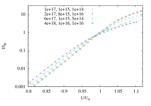
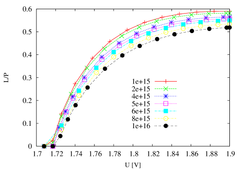
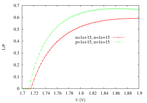
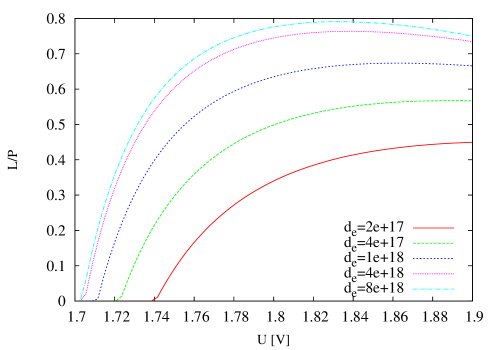
The above function is continuous at , as it obviously should, but it’s derivative is usually not. We used Equation (1) to find out and . However, the accuracy of this method was found lower than accuracy of the following two methods described. Figure 1 shows a few typical examples of I(U) dependencies, together with lines computed to fit them by using (1).
Let us notice that since (1) may have a discontinuous derivative, using it to find out differential resistance at is ambiguous. From Equation (1), at , we will have on the side and on the side .
In fact, the differential resistance measured in experiments is, to some extend, determined by the resistance of buffer layers and contacts, and by the way how it has been actually defined for non-linear curves.
In practice, the dependence, above but not far above, may be asummed to be a linear function. In such a case, we find from data anaylysis, for the third dataset, for instance, in Figure 1, , which, together with computed contact resistance gives good qualitative agreement with the differential resistance expected for real laser, as listed in Table 2.
3.3.2 from maximum of .
Another approach to find is by finding position of maximum in derivative of logarithm of versus voltage: . This is a very accurate method when there is a sufficiently large number of datapoints available near . However, for that, we would have to perform a lot of computations that are time consuming, in small enough steps in . Hence, this method is not always effective.
3.3.3 from gain versus voltage curves.
We find that a good accuracy of determining is from extrapolating linearly gain versus voltage curve in a near range of voltage values below , to the value of maximal gain, which is constant above . The results presented in this paper were obtained that way.
3.4 Differential resistance and optical efficiency.
Let us use the simplified assumption that is linear above : . Together with linear dependence of lasing light power versus current, , we have the following relation between optical power efficiency, , and current :
| (2) |
Equation 2 gives a resonably accurate qualitative description of . The parameter determining position and value of maximum, , is governed by factor . In a typical case, with , , and , we have .
We sometime prefer to use another form of Equation 2, where as a function of voltage is used:
| (3) |
where .
4 N-N waweguide structure.
By "N-N" waveguide structure we mean a doping structure as described in Table 1, where both waveguides and the active region (QW) are n-type doped.
We present here selected examples only of data obtained from semi-automatic analyses of thousands of datasets.
4.1 The role of doping in Active Region (QW).
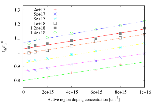
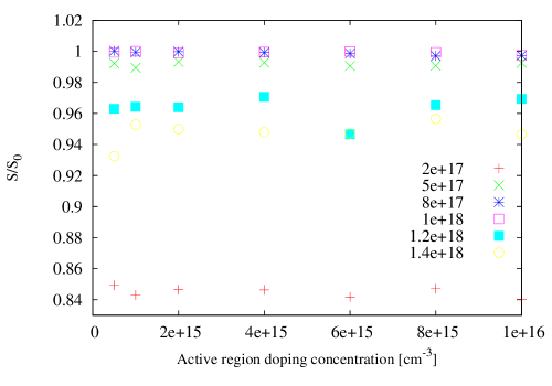
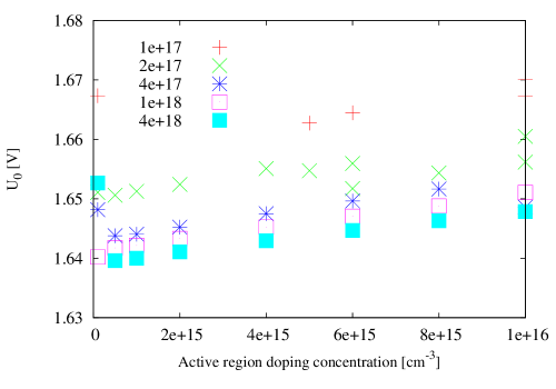
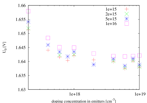
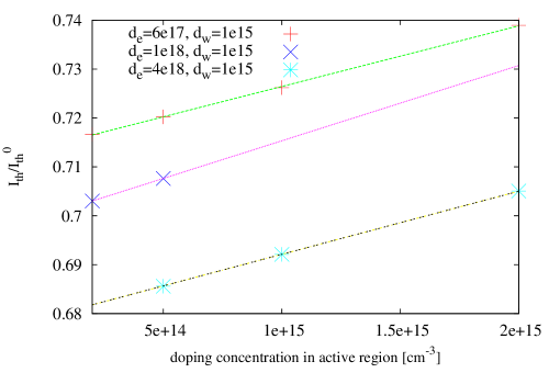
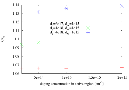
Figures 3, 4, and 5 show the role of doping concentration in active region, for a few values of doping concentrations in emitter regions, on basic characteristics of lasers: threshold current, slope of light power versus current, , and lasing offset voltage, respectively. The doping concentration in waveguide regions is the same on these three figures; it is .
We see that none of these quantities, i.e. , , , depends strongly on active region doping.
Therefore, it is not unexpected that the optical efficiency, the ratio of optical power to total power supplied to the laser, , as shown in Figure 6, weakly depends on doping concentration in active region as well. Though for the lower doping the higher optical efficiency is obtained.
4.2 The role of doping in Waveguide Regions.
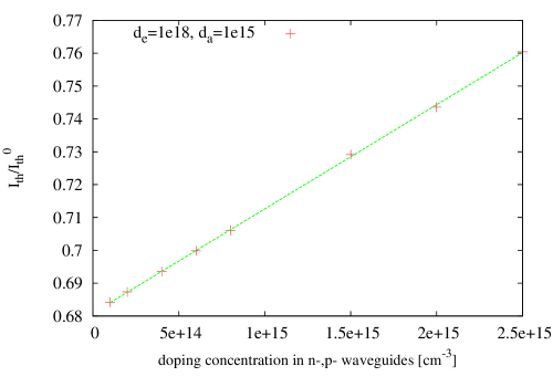
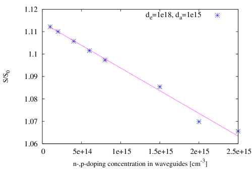
The effects of doping in waveguide regions are similar to these in the active region, but stronger.
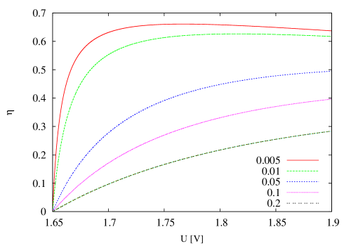
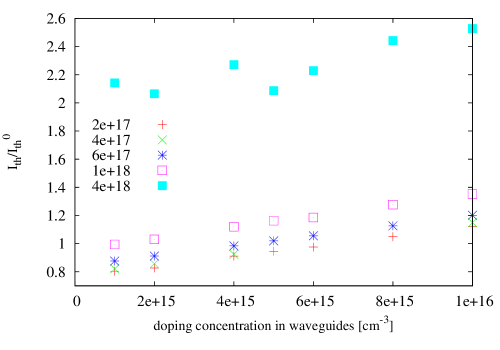
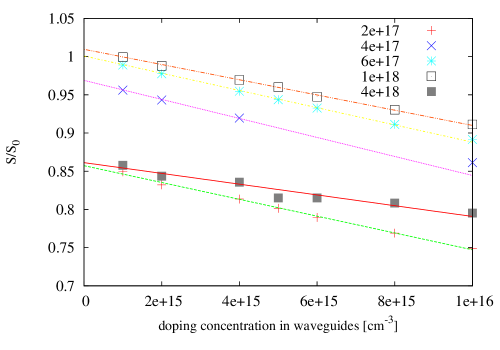
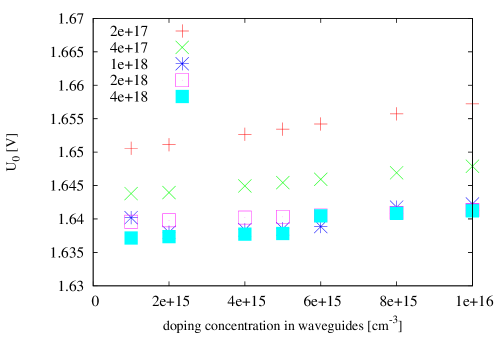
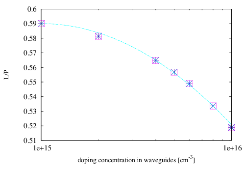
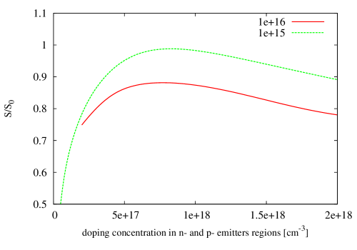
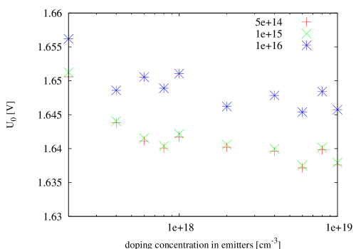
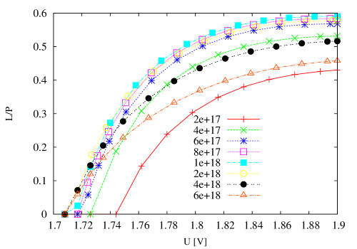
Figures 7, 8, 9, and 10 illustrate, respectively, dependencies of threshold currend, , lasing offset voltage , and optical efficiency on doping levels in waveguide regions. We observe, again, that the best characteristics (lowest and highest values) are at lowest doping levels in waveguides. also weekly depends on doping in waveguides. The most significant role is played by doping in emitters regions, rather. However, as Figure 10 shows, optical efficiency changes significantly with doping levels. One would like here to use Equation 3 to describe the data in this Figure. However, it could provide only a very qualitative fiting of the data. Since all the data in this figure indicate on the same or very close values of (compare also results of Figure 9), we attribute large differences between these curves to significant increase of differential resistance when doping level increases. And that could be understood as building up of p-n junction outside of quantum well region, with increase of doping.
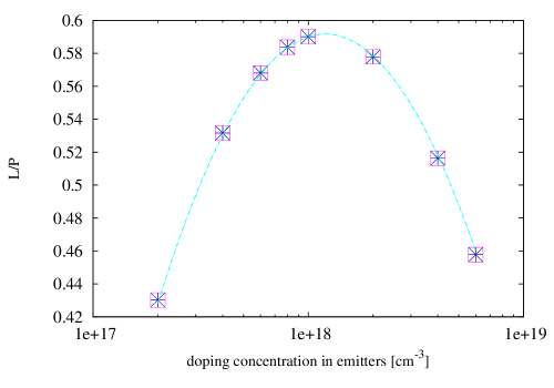
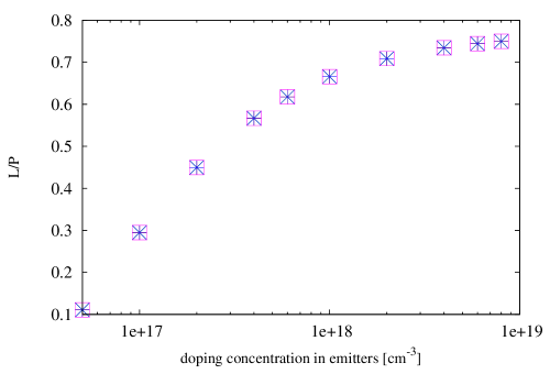
A characteristic for "N-N" structure is parabolic dependence of optical efficiency on doping levels, as shown in Figure 11.
4.3 The role of doping in Emitters Regions.
Doping levels in emitters regions contribute in the most prominent degree to laser characteristics.
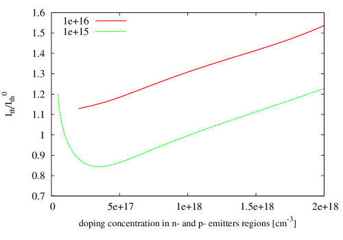
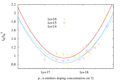
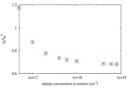
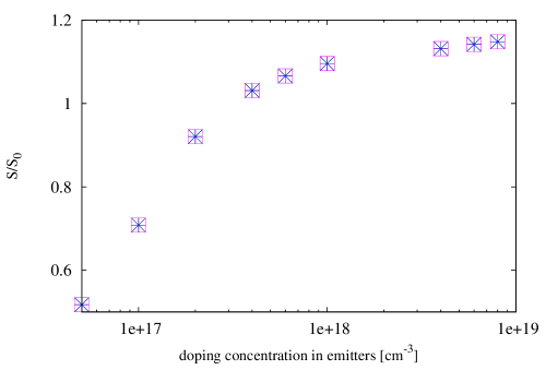
Figures 12 and 13 show typical example dependencies of and on doping in emitters. Clearly is observed a minimum in at somewhat lower than , and a maximum in at a value of close to that but not the same.
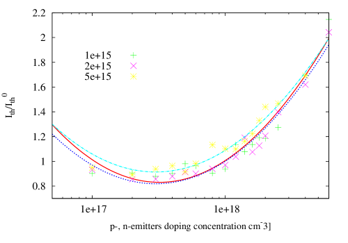
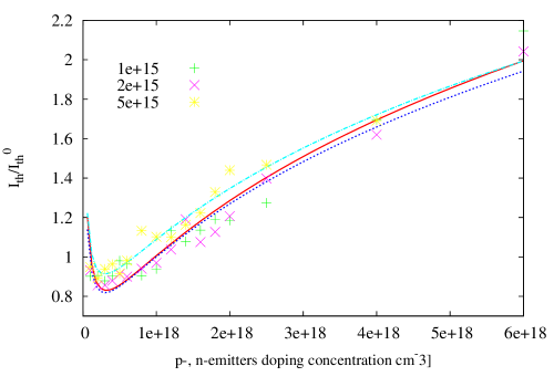
In Figures 14, 15 and 16, we show the presence of such a minimum in for a few more sets of data. We show that a parabolic dependence (when doping concentration is drawn on logarythmic axes) is a good approximation of the data: compare the same results as in Figure 15 shown however in linear scale in Figure 16:
| (4) |
where , , and are certain fiting parameters.
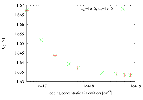
The lasing offset voltage (Figures 17 and 18) is sensitive to emitters doping at low levels, only, below around .
Strong dependencies of and on doping manifest itself in a strong dependence of optical efficiency on doping levels, as Figure 19 shows. Again, it has a parabolic character (Figure 19), similar to that one found for waveguides (Figure 11).
5 N-P waveguide structure.
By "N-P" waveguide structure we mean a doping structure that differes from that described in Table 1, where both waveguides and the active region (QW) are n-type doped. Here we assume that the waveguide on the side of n-emitter is of n-type, the other one is of p-type, and QW doping is of n-type.
The most remarkable difference between N-N and N-P structures is that in case of the last one a large reduction of and a significant increase in and in optical efficiency are found.
5.1 Active region doping
.
Figures 21 and 21 show the role of doping concentration in active region, for a few values of doping concentrations in emitter regions, on basic characteristics of lasers: threshold current and slope of light power versus current, , respectively.
We see that none of these quantities depends strongly on active region doping. These effects are similar to the onse observed for "N-N" type of waveguide structure.
5.2 Waveguides doping
.
The effects of doping in waveguide regions are much stronger for N-P structure than these reported for N-N one.
Both, lasing threshold current (Figure 23) and corresponding (Figure 23) show a nice strong linear dependence on waveguides doping. Since the first one has a positive slope and the second one negative, there will no maximum as a function of in this case, which is different that for the case of N-N structure.
The lasing offset voltage corresponding to the data displayed in Figures 23 and 24 does not change with waveguide doping (within the accuracy of our modeling, and the studied doping range), and it is of the value of .
In Figure 25 we compare optical efficiency for both types of structures.
5.3 Doping in Emitters
.
As in case on N-N structures, here also doping levels in emitters regions contribute the most to laser characteristics.
Figures 26 and 26 show example dependencies of and on doping in emitters. There are no maxima/minima there like in case of N-N structure, and at concentrations above about the effect of doping becomes small.
The lasing offset voltage (Figure 28) is sensitive to emitters doping at low levels, only, below around . This is the same as for N-N structure.
Optical efficiency does depend weekly on doping at large doping levels, unlike for N-N structures (Figures 29 and 30).
6 Summary and Conclusions.
SCH AlGaAs lasers with two kinds of waveguide doping structures have been modeled with Synopsys TCAD: "N-N" type structure where both waveguides have n-type of doping (with QW doping of n-type as well), and "N-P" structure where the waveguide on the side of p-emitter has p-type doping. The "N-N" structure is of the type we have experimental data for and it was used as a reference in our calculation calibration.
We observed that the doping level in active region has a small only influence on laser characteristics (lasing threshold current, slope of light power versus current, lasing offset voltage, optical efficiency). Better results are obtained for the lowest possible doping. More pronounced influence is of doping in waveguide regions. For "N-N" type of structure an optimal doping level is of around , but for "N-P" type of structure, it is desirable to have lower level of doping concentration there.
The most significant is the role of doping levels in emitters. It should be around in case of both types of structures. However, "N-P" type of structure gives significantly better results than "N-N" one, with threshold current lowered to about 70% and optical efficiency increased to near 80%.
References
- [1] Zh. I. Alferov, The double heterostructure concept and its applications in physics, electronics, and technology, Rev. Mod. Phys. 2001. V.73. No.3. P.767-782.
- [2] S. I. Matyukhin, Z. Koziol, and S. N. Romashyn, The radiative characteristics of quantum-well active region of AlGaAs lasers with separate-confinement heterostructure (SCH), arXiv:1010.0432v1 [cond-mat.mtrl-sci] (2010)
- [3] Z. Koziol, S. I. Matyukhin, Waveguide profiling of AlGaAs lasers with separate confinement heterostructures (SCH) for optimal optical and electrical characteristics, by using Synopsys’s TCAD modeling, unpublished.
- [4] Z. Koziol, S. I. Matyukhin, and S. N. Romashyn, Non-monotonic Characteristics of SCH Lasers due to Discrete Nature of Energy Levels in QW, accepted for presentation at Nano and Giga Challenges in Electronics, Photonics and Renewable Energy Symposium and Summer School, Moscow - Zelenograd, Russia, September 12-16, 2011
- [5] A. Yu. Andreev, S. A. Zorina, A. Yu. Leshko, A. V. Lyutetskiy, A. A. Marmalyuk, A. V. Murashova, T. A. Nalet, A. A. Padalitsa, N. A. Pikhtin, D. R. Sabitov, V. A. Simakov, S. O. Slipchenko, K. Yu. Telegin, V. V. Shamakhov, I. S. Tarasov, High power lasers ( = 808 nm) based on separate confinement AlGaAs/GaAs heterostructures, Semiconductors, 2009, 43(4), 543-547.
- [6] A. V. Andreev, A. Y. Leshko, A. V. Lyutetskiy,A. A. Marmalyuk, T. A. Nalyot, A. A. Padalitsa, N. A. Pikhtin, D. R. Sabitov, V. A. Simakov, S. O. Slipchenko, M. A. Khomylev, I. S. Tarasov, High power laser diodes ( = 808 – 850 nm) based on asymmetric separate confinement heterostructure, Semiconductors, 2006 40(5), 628-632.
- [7] Sentaurus Device User Guide, Synopsys, 2010, www.synopsys.com