Gap Anisotropy in Iron-Based Superconductors: A Point-Contact Andreev Reflection Study of BaFe2-xNixAs2 Single Crystals
Abstract
We report a systematic investigation on -axis point-contact Andreev reflection (PCAR) in BaFe2-xNixAs2 superconducting single crystals from underdoped to overdoped regions (0.075 ). At optimal doping () the PCAR spectrum feature the structures of two superconducting gap and electron-boson coupling mode. In the scenario, quantitative analysis using a generalized Blonder-Tinkham-Klapwijk (BTK) formalism with two gaps: one isotropic and another angle dependent, suggest a nodeless state in strong-coupling limit with gap minima on the Fermi surfaces. Upon crossing above the optimal doping (), the PCAR spectrum show an in-gap sharp narrow peak at low bias, in contrast to the case of underdoped samples (), signaling the onset of deepened gap minima or nodes in the superconducting gap. This result provides evidence of the modulation of the gap amplitude with doping concentration, consistent with the calculations for the orbital dependent pair interaction mediated by the antiferromagnetic spin fluctuations.
pacs:
74.20.Rp, 74.25.Ha, 74.70.DdIt is generally accepted that superconductivity in iron pnictides results from a superexchange repulsion mediated by magnetic excitations, which couple electron and hole pockets of the Fermi surface MazinPRL ; LeeDH ; Kuroki . Such pairing interactions favor either isotropic -wave order parameters with opposite signs on different sheets of the Fermi surface (FS)( model) or anisotropic -wave or even -wave order parameters with nodes Kuroki2 ; Graser . Consensuses have been reached on several systems, e. g. LaFePO Flet , KFe2As2 LiSY , BaFe2(As1-xPx)2 Hashi , and so on, that nodes exist on the gap structure. However, experimental confirmations of such a nodal-gap state remains highly controversial in other systems DingH ; ARPES ; ZhangXH ; Hardy ; Taillefer ; Prozorov1 ; Prozorov2 ; Imai ; MuG ; Fukazawa ; Raman ; WuD . For example, measurements of the electronic specific heat of Ba(Fe1-xCox)2As2 have shown a field dependence consistent with both a fully gapped FS Hardy and a nodal quasiparticals at the Fermi level Imai ; MuG . Such scattered experimental results and interpretations may come from the different qualities and doping level of the samples studied.
Point-contact Andreev reflection (PCAR) spectroscopy has been adopted for probing the density of state (DOS) of superconductors with the high energy resolution. In addition, the capability of this technique to study the anisotropy and the temperature dependence of the superconducting gap make it a unique tool in providing invaluable information for various mechanisms of unconventional superconductivity (for a review, see Refs. 21, 22). Several theoretical calculations have been reported on the PCAR conductance characteristics of a junction involving the symmetry in iron pnictide superconductors Golubov ; WangQH . However, due to the long-standing issue of surface or/and interface degradation, experimental results by PCAR technique reveal a wide variation in the measured Andreev conductance spectra and consequently, the gap values, especially for the case of -axis junctions Sameuley ; LGreene . In this Letter, we fabricate highly transparent -axis direct contacts to perform the PCAR spectroscopy study on a series of electron-doped BaFe2-xNixAs2 single crystals over a wide doping range. The conductance spectra show a systematic and consistent behavior with the variation of the doping level, indicative of a doping dependence of the order parameter for Ni-122 superconductor. In the scenario, by using a generalized two-gap Blonder-Tinkham-Klapwijk (BTK) model, we estimate the gap amplitude on the hole and electron FS sheets.
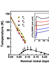
High-quality single crystals of BaFe2-xNixAs2 were grown from a self-flux method, as described elsewhere Luo . The crystals were characterized using x-ray diffraction and energy dispersion (EDX). The doping level in the crystals was determined by inductive coupled plasma emission spectrometer (ICP), which gave a Ni concentration roughly 0.8 times the nominal content . We choose five compositions: underdoped, =0.075 (UD13), 0.085 (UD17); overdoped, with =0.12 (OD18), 0.15 (OD14), and optimally doped with (OP20). The typical level of impurity phases has been checked by specific heat measurement on the optimally doped crystal , in which a residual component at revealed an impurity phases of Wen-Ni . The temperature dependence of resistivity for these five compositions under investigation is displayed in inset of Fig. 1, by which the bulk transition temperature is determined (95% of the normal state resistivity) for each composition. Consequently, the value for each composition is shown on the phase diagram in the main panel of Fig. 1.
Point contacts to the flat and shiny surfaces cleaved along the -axis of BaFe2-xNixAs2 crystals were made using thick silver paste (4929N DuPont) bonding with gold wires (of 16 m diameter). The typical size of these planar contact is about 0.08-0.15 mm under a microscope. Due to the nanocrystalline nature of the silver paint, the contact made in this way, is actually formed by many nanocontacts analog to tip point-contact technique Italy . For the backside electrical wiring, we applied ultrapure indium or silver paste to cover the whole area of the bottom surfaces of the crystals. On each piece of the crystal, 5-6 planar contacts were made from point to point to ensure the reproducibility and consistency of the junction conductance spectra and their spectroscopic nature.
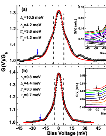
Fig. 2(a) and (b) show the raw (inset) and normalized conductance curves of two -axis Ag/BaFe1.9Ni0.1As2 point contacts (OP20a and OP20b), respectively. The contacts made in this way remain stable in thermal cycling, and the contact resistance at high bias varies very little (%) over the whole range up to . The Andreev signal as the conductance enhancement decreases on increasing and vanishes at , leaving a slightly asymmetrical -shaped normal state. Shown in the main panels of Fig. 2(a) and (b), the magnitude of the Andreev reflection reaches as high as 30%-40%, implying a relatively transparent boundary between Ag nanoparticle and BaFe2-xNixAs2 superconductors. The stabilities in and the high level of Andreev signal indicate that the conduction channels through the contact is in ballistic regime, and therefore, energy-resolved spectroscopy is possible. A feature shows up in these conductance curves: an additional peak at mV, and the peak gradually disappears with approaching . It seems that this peak is much pronounced when the Andreev signal is relatively low, which is close to the case of tunneling side (see below). Very recently, this conductance peak at the edge of the gap has been observed in Co-122 crystals Italy2 , and is attributed to the signature of an electron-boson coupling associated with the superconducting gap. The observation of the electron-boson coupling mode in the conductance spectra implies the high quality of the point-contacts and thus their spectroscopic nature.
The two-gap superconductivity manifests itself as a “kink” in the in-gap conductance, marked at the dashed lines in Fig. 2 (a) and (b). To explicitly describe the variety of spectral behavior observed and quantitatively resolve the gap amplitude, we invoke a generalized BTK formula BTK with three parameters: a dimensionless parameter which represents the interface transparency; an imaginary quasiparticle energy modification Dynes which reflects the spectral broadening, and the superconducting gap . In BTK model, the normal and Andreev reflection probabilities, respectively, are related to the DOS of the superconductor with the normal-state DOS and the crystalline angle parallel to the current injection. To choose a gap function to calculate these two-gap conductance spectra, we assume, based on the scenario, an isotropic gap and an anisotropic gap of the general form , with the gap anisotropy ratio varying from (isotropic state) to (completely -wave) Chubukov ; MazinRaman ; WuD . Therefore, by the standard two component conductance (current) model the conductance spectra is the contributions of the hole-like () and electron-like () Fermi pockets: , where is the spectral weight. For simplicity, we assume a balanced contribution of hole and electron Fermi surfaces to the spectral conductance by taking =0.5.
Examples of normalized curves and their fits at K are shown in the main panels of Fig. 2(a) and (b) for junctions OP20a and OP20b, respectively. The two-gap BTK model (red lines) fit very well the main features of the experimental curves except the electron-boson coupling mode around 20 meV, yielding a set of fitting parameters associated with gap magnitude and anisotropy ratio: meV, =4.2, and =0.3 for OP20a and meV, meV, and =0.3 for OP20b, respectively. It is noted that the same gap magnitude is also extracted from a recent PCAR experiment on a -axis Ag/BaFe1.8Co0.2As2 with the comparable K Italy2 . Here we emphasize that a two-gap formula with two -wave gap () can also fits our experimental data rather well. However, the parameters are applied to fulfill the fit at this low , which brings a large uncertainty in the gap magnitude.
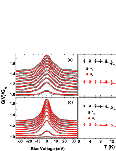
With these fitting parameters, we check the validity of these fits by extending the fit to the overall temperature spectral. As shown in Fig. 3(a) and (c), the two-gap model still fits reasonably well the -dependence of these curves with fitted gap magnitude. In this overall- spectral fit, and are constant with while and meV (OP20a) and and meV (OP20b) are almost constant or slightly increase with . From the fits of various curves we obtain the gaps and as a function of , which is plotted in Fig. 3(b) and (d) for these two junctions, respectively. For comparison, the obtained gaps can be approximated by an empirical gap formula: with for and 1.86 for (cf. for weak-coupling BCS gap).
We analyze the physical meanings of the obtained gap values and gap function. It is shown from angle-resolved photoemission spectroscopy experiment on a Co-122 crystal that the large gap is located on the hole FS sheet, instead, the small gap is presented on one of the electron FS sheets ARPES . The gap values and , both above the BCS weak-coupling ratio. Besides, the value from the function also points to a strong-coupling character for both (hole FS) and (outer electron FS). These results are consistent with a three-band Eliashberg model threeTHY , in which spin fluctuations mainly provide the interband coupling, and thus so in the electron-boson coupling matrix. On the other aspect, the existence of strong electron-boson coupling in this compound is manifested by the observation of the spectral peak at about 20 mV. In our low-transparency (large for OP20a) point contact, a characteristic energy of meV and 11 meV (OP20b junction with small ). This energy scale is compatible with the spin-resonance energy observed by neutron scattering on the same crystals a1 .
The obtained anisotropy ratio , resolved in our -axis PCAR spectroscopy of BaFe1.9Ni0.1As2, indicates a full gap state with gap minima along axis. This nodeless state of optimally doped Ni-122 is in similarity with that of optimally-doped Co-122, in which a gap minima is already present at maximal by the -axis thermal conductivity measurements Taillefer ; Taillef .
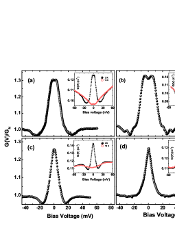
It is natural, however, to inspect the manner of the superconducting gaps in the crystals with doping away from the optimum. We have measured the point-contact curves in whole range up to for junctions with (UD13), 0.085 (UD17), 0.12 (OD18), and 0.15 (OD14). The typical curves at K () and are shown in Fig. 2(a)-(d) for these four samples respectively. As shown, these curves exhibit a consistent behavior: 1) An underlying feature of a dominant single gap is unambiguously identified with a similar conductance enhancement of 25%-35% for each junction; 2) A parabolic normal-state curve with a slight asymmetry at for each , opposite to those of hole-doped K-122 LGreene ; ZhangXH , implies the similar origin of the underlying normal-state background. Nevertheless, a striking feature in these normalized (and the raw) curves is that: at K, a conductance plateau and/or a double peak around zero bias for junctions UD13 and UD17 gradually evolutes into an in-gap sharp peak in for junctions OD18 and OD14. Considering the overall spectral consistency in these junctions, the systematic evolution of the Andreev conductance spectra with doping concentration is nontrivial. Qualitatively, for highly transparent junctions at finite , the appearance of an in-gap plateau in Andreev conductance spectrum is a signature of a fully gapped state. In contrast, an in-gap conductance peak is a characteristic of an anisotropic gap state due to the presence of a finite DOS at low energy, like a -wave gap in cuprates Deutscher . We note that it is not easy to describe the spectral behavior using simple formulism, because we are dealing with multi-band or/and even multi-gap system. Therefore, our observation that the systematic evolution from the in-gap conductance plateau for the underdoped samples to the in-gap peak in curves for the overdoped samples indicates the existence of doping induced evolution of superconducting gaps with an isotropic feature in the underdoped region to an anisotropic, even, nodal gap in the overdoped side. This is highly consistent with the result of the -dependent penetration depth in a series of Ni-122 superconductors, in which with the exponent for underdoped samples and becomes more linear- dependent for overdoped samples, indicating the development of nodal gaps in the overdoped region Prozorov1 .
In conclusion, measurements on point-contact junctions made on single crystals of BaFexNi1-xAs2 illustrate an interesting evolution of the gap structure. The Andreev conductance spectra clearly show a full-gap state for underdoped crystals and a highly anisotropic, perhaps nodal-like gap state for overdoped crystals. Quantitative analysis of the spectral data of optimally-doped contacts using a generalized BTK formalism resolves two superconducting gaps in strong coupling limit. Resulted from the analytical fitting, the small gap on the electron-like FS sheets shows a crossover from a nodeless in the underdoped side to a nodal feature in the overdoped region. This result provides evidence of the modulation of the gap amplitude on the FS with doping concentration, consistent with the calculation for the orbital dependent pair interaction mediated by the antiferromagnetic spin fluctuations.
Acknowledgement: The authors are grateful to Profs. R. Prozorov, Qiang-Hua Wang and Dr. Gang Mu for intensive discussions. This work is supported by the National Science Foundation of China, the Ministry of Science and Technology of China (973 project No: 2011CBA00100), and Chinese Academy of Sciences (Project ITSNEM).
cong_ren@iphy.ac.cn
References
- (1) I. I. Mazin et al., Phys. Rev. Lett. 101, 057003 (2009).
- (2) F. Wang et al., Phys. Rev. Lett. 102, 047005 (2008).
- (3) K. Kuroki et al., Phys. Rev. Lett. 101, 087004 (2008).
- (4) K. Kuroki et al., Phys. Rev. B 79, 224511 (2009).
- (5) S. Graser et al., Phys. Rev. B 81, 214503 (2010); T. A. Maier, et al., Phys. Rev. B 79, 224510 (2009).
- (6) D. Fletcher et al., Phys. Rev. Lett. 102, 147001 (2009); C. W. Hick et al., Phys. Rev. Lett. 103, 127003 (2009).
- (7) J. K. Dong et al., Phys. Rev. Lett.104, 087005 (2009); K. Hashimoto et al., Phys. Rev. B 82, 014526 (2010).
- (8) K. Hashimoto et al., Phys. Rev. B 81, 220501 (2010).
- (9) H. Ding et al., EPL. 83, 47001 (2008).
- (10) K. Terashima et al., Proc. Natl. Acad. Sci. U.S.A. 106, 7330 (2009).
- (11) X. H. Zhang et al., Phys. Rev. Lett. 102, 147002 (2009); ibid. Phys. Rev. B 82, 020515(R) (2010).
- (12) F. Hardy et al., Phys. Rev. Lett. 102, 187004 (2009); ibid, arXiv:1007.2218.
- (13) J.-Ph Reid et al., Phys. Rev. B 82, 064501 (2010).
- (14) R. Prozorov et al., Phys. Rev. B 80, 174517 (2009).
- (15) C. Martin et al., Phys. Rev. B 81, 060505 (2010).
- (16) K. Gofryk et al., Phys. Rev. B 83, 064513 (2011).
- (17) G. Mu et al., arXiv: 1103.1300 (2011).
- (18) H. Fukazawa et al., J. Phys. Soc. Jpn 78, 033704 (2009).
- (19) B. Muschler et al., Phys. Rev. B 80, 180510(R) (2009).
- (20) E. Schachinger, and J. P. Carbotte, Phys. Rev. B 80, 174526 (2009); D. Wu, et al., Phys. ReV. B 82, 184527 (2010).
- (21) G. Deutscher, Rev. Mod. Phys. 77, 109 (2005)
- (22) D. Daghero, and R.S. Gonnelli, Supercond. Sci. Technol. 23, 043001 (2010).
- (23) A. A. Golubov et al., Phys. Rev. Lett. 103, 077003 (2009); P. Ghaemi, F. Wang, and A. Vishwanath, Phys. Rev. Lett. 102, 157002 (2009).
- (24) Da Wang, Yuan Wan, and Qianh-Hua Wang, Phys. Rev. Lett. 102, 197004 (2009); I. B. Sperstad, J. Linder, and A. Sudbø, Phys. Rev. B 80, 144507 (2009). M. A. N. Araujo and P. D. Sacramento, Phys. Rev. B 79, 174529 (2009).
- (25) P. Samuely et al., Physica C 469, 507 (2009).
- (26) Xin Lu et al., Supercond. Sci. Technol. 23, 054009 (2009).
- (27) Yan-Chao Chen et al., SST 24, 065004 (2011).
- (28) Bing Zeng et al., arXiv:1006.2785.
- (29) M. Tortello et al., Phys. Rev. Lett. 105, 237002 (2010).
- (30) G. E. Blonder, M. Tinkham, and T. M. Klapwijk, Phys. Rev. B 25, 4515 (1982).
- (31) R. Dynes et al., Phys. Rev. Lett. 41, 1509 (1978).
- (32) A. V. Chubukov, M. G. Vavilov, and A. B. Vorontsov, Phys. Rev. B 80, 140515(R) (2009).
- (33) A. B. Vorontsov, and I. Vekhter, Phys. Rev. Lett. 105, 187004 (2010); I. I. Mazin, et al., Phys. Rev. B 82, 180502 (2010).
- (34) G. A. Ummarino et al., Phys. Rev. B 80, 172503 (2009); L. Benfatto, E. Cappelluti, and C. Castellani, Phys. Rev. B 80, 214522 (2009).
- (35) Miaoyin Wang et al., Phys. Rev. B 81, 174524 (2010).
- (36) M. A. Tanatar et al., Phys. Rev. Lett. 104, 067002 (2010).