Controlled fabrication of single-walled carbon nanotube electrodes by electron-beam-induced oxidation
Abstract
The fabrication of metallic single-walled carbon nanotube electrodes separated by gaps of typically 20 nm width by electron-beam-induced oxidation is studied within an active device configuration. The tube conductance is measured continuously during the process. The experiment provides a statistical evaluation of gap sizes as well as the electron dose needed for gap formation. Also, the ability to precisely cut many carbon nanotubes in parallel is demonstrated.
I Introduction
In recent experiments, individual carbon nanotubes have been used as true nanoscale electrodes for contacting different types of materials such as nanocrystalsP. Qi, A. Javey, M. Rolandi, Q. Wang, E. Yenilmez and H. Dai (2004), single moleculesX. Guo, J.P. Small, J.E. Klare, Y. Wang, M.S. Purewal, I.W. Tam, B.H. Hong, R. Caldwell, L. Huang and S. O’Brien (2006); C.W. Marquardt, S. Grunder, A. Blaszscyk, S. Dehm, F. Hennrich, H.v. Löhneysen, M. Mayor and R. Krupke (2010), and phase-change materialsF. Xiong, A. Liao, D. Estrada and E. Pop (2011). The carbon nanotube electrodes were thereby fabricated by making gaps in pristine nanotubes either using current-induced oxidation or plasma oxidation through masks. A challenge to those techniques is the limited reliability in fabricating small and reproducible gap sizes. Recently it has been shown that nanogaps in carbon nanotubes can be formed by electron-beam-induced oxidation within a scanning electron microscopeT.D. Yuzvinsky, A.M. Fennimore, W. Mickelson, C. Esquivias and A. Zettl (2005); P. Liu, F. Arai and T. Fukuda (2006); P.S. Spinney, D.G. Howitt, S.D. Collins, R.L. Smith (2009). However, this technique has not been used to fabricate single-walled carbon nanotube (SWNT) electrodes within a device geometry. Also the detailed mechanism that leads to gap formation remains vague. In this work, we study the process of gap formation in metallic SWNTs (mSWNTs) within a three-terminal device configuration by electron-beam-induced oxidation (EBIO), while simultaneously measuring the tube conductance. The experiment provides the critical dose for gap formation, a statistical evaluation of the gap size, and identifies the type of electrons that lead to local oxidation.
II Experimental Details
Devices were fabricated on a degenerately doped silicon backgate with 800 nm of thermal oxide and on 50 nm thick Si3N4 membranes of 50 x 50 µm2 lateral size, supported by a silicon substrate frame. 200 nm wide contacts were prepared by standard electron-beam lithography and metallization with 5 nm titanium and 50 nm palladium. The gap between metallic contacts was adjusted to the length distribution of the nanotube dispersion and was typically 700 nm wide.
mSWNTs were prepared by pulsed laser vaporization followed by sonication in 1 wt% sodium cholate in D2O and subsequent sorting using density-gradient centrifugation and size-exclusion chromatography as has been reported elsewhereS. Lebedkin, P. Schweiss, B. Renker, S. Malik, F. Hennrich, M. Neumaier, C. Stoermer and M.M. Kappes (2002); M.C. Hersam (2008); K. Moshammer, F. Hennrich and M.M. Kappes (2009). mSWNTs with a diameter distribution of 1.20.2 nm and a length of 1 0.5 m were used for the nanogap devices.
mSWNTs were deposited onto the metal contacts by dielectrophoresisA. Vijayaraghavan, C. Sciascia, S. Dehm, A. Lombardo, A. Bonetti, A.C. Ferrari and R. Krupke (2009). For the single-tube devices, a peak-to-peak voltage of Vpp = 1.5 V and a frequency of f = 300 kHz were used for a duration of 3 minutes, while a drop of nanotube dispersion with a concentration of 5 nanotubes per m3 was placed onto the device. For the fabrication of mSWNT thin-film devices, a discontinuous alternating voltage with Vpp = 6 V, ton = 10 ms and toff = 90 ms was used to prevent electroosmosis as explained in S. Blatt, F. Hennrich, H.v. Löhneysen, M.M. Kappes, A. Vijayaraghavan and R. Krupke (2007).
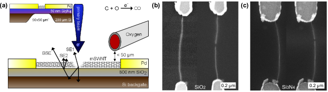
Imaging and cutting of the nanotubes were carried out in a Zeiss Ultra Plus scanning electron microscope, with the experimental setup shown in Fig. 1a. The built-in charge compensation module was used to inject oxygen gas (purity 99.998 %) through a needle of 500 m diameter. The lateral position of the tip of the needle was adjusted at 200 m off the center of the electron-beam scan window, while its vertical position was fixed to less than 50 m above the device surface.
Gas flow rate into the microscope was monitored by a mass flow controller and set to 35 2 sccm/min at a system pressure of 5.7 10-3 mbar. Molecular flux at the exit of the needle was calculated to 8 107 nm-2s-1. The local pressure at that point was estimated to 1 mbar. A Keithley 2636A two-channel source measure unit was used in combination with two MM3A-EM Kleindiek nanoprobers mounted inside the electron microscope for in-situ electrical characterization of the nanotube contacts.
Initially, the devices were current-annealed in vacuum to release charges trapped in the substrate from the lithographic fabrication of the contactsC.W. Marquardt, S. Dehm, A. Vijayaraghavan, S. Blatt, F. Hennrich and R. Krupke (2008). The current-annealed mSWNT devices showed linear current-voltage (I-V) curves and no gate dependence. I-V curves were measured before and after EBIO gap formation. During the EBIO process a constant source-drain voltage VSD of maximum 1 V was applied and the current continuously measured in intervals of 50 ms.
To cut the carbon nanotubes an electron-beam line scan was executed across the nanotube while injecting the oxygen. During line scans the microscope magnification was adjusted to be either 25 kX or 50 kX, yielding a line scan width of 4.57 m and 2.29 m, respectively. The primary electron-beam current used was 100 pA, which yields a line dose of 21.8 C/m and 43.7 C/m per second, respectively. Acceleration voltage of the primary electrons (PEs) was set to 10 kV. Scale-calibrated images were used to assess reproducibility of gap sizes.
III Results and Discussion
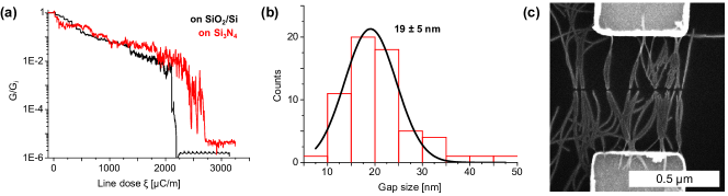
Fig. 1b shows SEM images of an individual mSWNT on SiO2/Si before (left) and after (right) EBIO-induced gap formation. The images were recorded with an in-lens detector that is expected to be sensitive to SE1 and SE2 secondary electronsJ. Frosien, S. Lanio and H.P. Feuerbaum (1995). For better visibility of the mSWNT, we used voltage-contrast scanning electron microscopy (VCSEM) to suppress the SEs of the SiO2/Si substrateA. Vijayaraghavan, S. Blatt, C.W. Marquardt, S. Dehm, R. Wahi, F. Hennrich and R. Krupke (2008). The required backgate voltage Vg = +10 V was applied with respect to the source-drain electrodes only for imaging. An effect of Vg on the EBIO process was not observed. The EBIO-induced gap shown in Fig. 1b is 20 nm wide. This is a typical result since the gap size average over 62 devices on SiO2/Si substrates is (19 5) nm, as shown in Fig. 2b. Similar results were also obtained with mSWNTs on 50 nm thick Si3N4 membranes. Fig. 1c shows such a device on Si3N4 before (left) and after (right) EBIO-induced gap formation. Although recorded without VCSEM, the membrane appears dark due to its limited SE2 generationGoldstein et al. (2003). We should note that the formation of a gap has also been confirmed by topography measurements with an atomic force microscope (not shown). The critical line dose ξC that is required for gap formation has been determined from in-situ conductance measurements. Fig. 2a shows the typical conductance reduction of a mSWNT-device on SiO2/Si and Si3N4, during the EBIO process. The traces of the conductance G have been normalized to their initial values Gi, at the beginning of the EBIO process at t = 0. Gi is typically on the order of (40 kΩ)-1 after current-annealing. G decreases with ξ almost exponentially by two orders of magnitude, before a sudden drop by additional 3-4 orders of magnitude down to the electron-beam-induced residual conductance is recorded (10 GΩ)-1. This last step indicates the formation of a gap in the nanotube. There are no plateaus in G which could indicate a step-wise introduction of defects. Typically ξC is on the order of a few mC/m. This behavior is in marked contrast to the continuous electron-beam-induced metal-to-insulator transitions, which are caused by charges trapped in the substrate surfaceC.W. Marquardt, S. Dehm, A. Vijayaraghavan, S. Blatt, F. Hennrich and R. Krupke (2008). It has been shown that such transitions require a line dose of 200 µC/m at 10 kV PE energy. During the EBIO process, such a small dose causes only a small reduction in G (see Fig. 2a), and cutting of tubes requires a dose which is ten times as high. We assume that charging is not important here since oxygen ions can compensate electron-beam-induced surface charges. Note also that it has been shown that trapped charges can be released under large bias and that the original conductance can be fully restored (reversibility)C.W. Marquardt, S. Dehm, A. Vijayaraghavan, S. Blatt, F. Hennrich and R. Krupke (2008). In the present case - due to the gap formation - the conductance drop remains irreversible even at VSD 10 V.
We now want to discuss the mechanism that leads to gap formation. Direct knock-on damage can be excluded, as the threshold for carbon nanotubes is 85 keVB.W. Smith and D.E. Luzzi (1999), much higher than the electron energies used in this and in previous workT.D. Yuzvinsky, A.M. Fennimore, W. Mickelson, C. Esquivias and A. Zettl (2005). We have also tested the use of argon instead of oxygen, but could not open a gap. It is likely that oxygen radicals forming under the electron beam are causing the gap formation. The lack of a significant difference between EBIO on a thick SiO2/Si substrate and a thin Si3N4 membrane implies that backscattered electrons (BSE) and BSE-generated secondary electrons (SE2) play a minor role since Monte Carlo simulations K.-P. Johnsen, C.G. Frase, H. Bosse and D. Gnieser (2010) showed that almost no electrons are backscattered from the Si3N4 membrane and its total SE yield (SE1 + SE2) is strongly reduced due to the absence of BSE and thus SE2. Moreover, the EBIO process appears to be insensitive to a suppression of SE1 and SE2 electrons by VCSEM. This indicates that the PEs are causing the gap formation.
A recent work on electron-beam-induced etching of SiO2 using XeF2 gasM.G. Lassiter and P.D. Rack (2008) indicates that the source of oxygen radicals is effectively limited to the area where the PE beam hits the surface, which for a line scan would be a strip of 1-2 nm width. What causes the gap to become 20 nm wide remains unclear at the moment. We assume that the gap acquires this large width either because of an exothermic chain reaction where the gap size is determined by the oxygen partial pressure in the systemC.W. Marquardt, S. Grunder, A. Blaszscyk, S. Dehm, F. Hennrich, H.v. Löhneysen, M. Mayor and R. Krupke (2010), or due to the diffusion of oxygen radicals. In both cases a variation of the pressure should have an influence on the gap size, which will be investigated in the future.
As an interesting final observation, we note EBIO is not limited to the cutting of individual nanotubes, but can also be extended to form gaps in devices with multiple nanotubes. Fig. 2c shows such an example. The device which contains 50 mSWNTs was produced by pulsed dielectrophoresis. With EBIO, gaps of similar size can be produced in all of the nanotubes at the same relative position. Such a result cannot be obtained by current-induced oxidationS. Shekhar, P. Stokes and S.I. Khondaker (2011); S. Shekhar, M. Erementchouk, M.N. Leuenberger and S.I. Khondaker (2011); D. Estrada and E. Pop (2011).
IV Conclusions
Reliable and lithographically precise fabrication of SWNT electrodes by electron-beam-induced oxidation was demonstrated for individual SWNT and SWNT thin-film devices. Nanogaps can be fabricated reliably down to a size of 19 5 nm. The independence of the gap size of the choice of substrate and of the number of secondary electrons suggests that the process is driven by primary electrons. Although the gaps produced by EBIO are still large compared to molecular scales, they have an advantageous size for addressing phase-change materialsF. Xiong, A. Liao, D. Estrada and E. Pop (2011) where reproducible gap sizes are required to obtain reproducible switching properties.
References
- P. Qi, A. Javey, M. Rolandi, Q. Wang, E. Yenilmez and H. Dai (2004) P. Qi, A. Javey, M. Rolandi, Q. Wang, E. Yenilmez and H. Dai, J. Am. Chem. Soc. 126, 11774 (2004).
- X. Guo, J.P. Small, J.E. Klare, Y. Wang, M.S. Purewal, I.W. Tam, B.H. Hong, R. Caldwell, L. Huang and S. O’Brien (2006) X. Guo, J.P. Small, J.E. Klare, Y. Wang, M.S. Purewal, I.W. Tam, B.H. Hong, R. Caldwell, L. Huang and S. O’Brien, Science 311, 356 (2006).
- C.W. Marquardt, S. Grunder, A. Blaszscyk, S. Dehm, F. Hennrich, H.v. Löhneysen, M. Mayor and R. Krupke (2010) C.W. Marquardt, S. Grunder, A. Blaszscyk, S. Dehm, F. Hennrich, H.v. Löhneysen, M. Mayor and R. Krupke, Nature Nanotechnology 5, 863–867 (2010).
- F. Xiong, A. Liao, D. Estrada and E. Pop (2011) F. Xiong, A. Liao, D. Estrada and E. Pop, Science 332, 568 (2011).
- T.D. Yuzvinsky, A.M. Fennimore, W. Mickelson, C. Esquivias and A. Zettl (2005) T.D. Yuzvinsky, A.M. Fennimore, W. Mickelson, C. Esquivias and A. Zettl, Appl. Phys. Lett. 86, 053109 (2005).
- P. Liu, F. Arai and T. Fukuda (2006) P. Liu, F. Arai and T. Fukuda, Appl. Phys. Lett. 89, 113104 (2006).
- P.S. Spinney, D.G. Howitt, S.D. Collins, R.L. Smith (2009) P.S. Spinney, D.G. Howitt, S.D. Collins, R.L. Smith, Nanotechnology 20, 465301 (2009).
- S. Lebedkin, P. Schweiss, B. Renker, S. Malik, F. Hennrich, M. Neumaier, C. Stoermer and M.M. Kappes (2002) S. Lebedkin, P. Schweiss, B. Renker, S. Malik, F. Hennrich, M. Neumaier, C. Stoermer and M.M. Kappes, Carbon 40, 417–423 (2002).
- M.C. Hersam (2008) M.C. Hersam, Nature Nanotechnology 3, 387–394 (2008).
- K. Moshammer, F. Hennrich and M.M. Kappes (2009) K. Moshammer, F. Hennrich and M.M. Kappes, Nano Res 2, 599–606 (2009).
- A. Vijayaraghavan, C. Sciascia, S. Dehm, A. Lombardo, A. Bonetti, A.C. Ferrari and R. Krupke (2009) A. Vijayaraghavan, C. Sciascia, S. Dehm, A. Lombardo, A. Bonetti, A.C. Ferrari and R. Krupke, ACS Nano 3, 1729–1734 (2009).
- S. Blatt, F. Hennrich, H.v. Löhneysen, M.M. Kappes, A. Vijayaraghavan and R. Krupke (2007) S. Blatt, F. Hennrich, H.v. Löhneysen, M.M. Kappes, A. Vijayaraghavan and R. Krupke, Nano Letters 7, 1960 (2007).
- C.W. Marquardt, S. Dehm, A. Vijayaraghavan, S. Blatt, F. Hennrich and R. Krupke (2008) C.W. Marquardt, S. Dehm, A. Vijayaraghavan, S. Blatt, F. Hennrich and R. Krupke, Nano Letters 8, 2767 (2008).
- J. Frosien, S. Lanio and H.P. Feuerbaum (1995) J. Frosien, S. Lanio and H.P. Feuerbaum, Nucl. Instr. and Meth. in Phys. Res. A 363, 25 (1995).
- A. Vijayaraghavan, S. Blatt, C.W. Marquardt, S. Dehm, R. Wahi, F. Hennrich and R. Krupke (2008) A. Vijayaraghavan, S. Blatt, C.W. Marquardt, S. Dehm, R. Wahi, F. Hennrich and R. Krupke, Nano Res 1, 321 (2008).
- Goldstein et al. (2003) J. Goldstein, D. Newbury, D. Joy, C. Lyman, P. Echlin, E. Lifshin, L. Sawyer, and J. Michael, Scanning electron microscopy and X-ray microanalysis (Springer, 2003) p. 205.
- B.W. Smith and D.E. Luzzi (1999) B.W. Smith and D.E. Luzzi, AIP Conf. Proc. 486, 360–363 (1999).
- K.-P. Johnsen, C.G. Frase, H. Bosse and D. Gnieser (2010) K.-P. Johnsen, C.G. Frase, H. Bosse and D. Gnieser, Proc. SPIE 7638, 76381O (2010).
- M.G. Lassiter and P.D. Rack (2008) M.G. Lassiter and P.D. Rack, Nanotechnology 19 (2008).
- S. Shekhar, P. Stokes and S.I. Khondaker (2011) S. Shekhar, P. Stokes and S.I. Khondaker, ACS Nano 5, 1739 (2011).
- S. Shekhar, M. Erementchouk, M.N. Leuenberger and S.I. Khondaker (2011) S. Shekhar, M. Erementchouk, M.N. Leuenberger and S.I. Khondaker, ArXiv e-prints (2011), arXiv:1101.4040 [cond-mat.mes-hall] .
- D. Estrada and E. Pop (2011) D. Estrada and E. Pop, Appl. Phys. Lett. 98, 073102 (2011).