Non-equilibrium inelastic electronic transport: Polarization effects and vertex corrections to the self-consistent Born approximation
Abstract
We study the effect of electron-vibron interactions on the inelastic transport properties of single-molecule nanojunctions. We use the non-equilibrium Green’s functions technique and a model Hamiltonian to calculate the effects of second-order diagrams (double-exchange DX and dressed-phonon DPH diagrams) on the electron-vibration interaction and consider their effects across the full range of parameter space. The DX diagram, corresponding to a vertex correction, introduces an effective dynamical renormalization of the electron-vibron coupling in both the purely inelastic and the inelastic-resonant features of the IETS. The purely inelastic features correspond to an applied bias around the energy of a vibron, while the inelastic-resonant features correspond to peaks (resonance) in the conductance. The DPH diagram affects only the inelastic resonant features. We also discuss the circumstances in which the second-order diagrams may be approximated in the study of more complex model systems.
pacs:
PACS numbers: 71.38.-k, 73.40.-c, 85.65.+h, 73.63.-bI Introduction
Junctions consisting of a single organic molecule between two metallic leads hold great promise for future nanoscale devices, where their potential applications include switches, transistors, and sensors. Experimentally, it has proved difficult to control their production in an atomistic manner, and so theoretical studies are crucial for a full understanding of their behaviour. It is known that inelastic effects play an important role in the behaviour of such devices Hipps and Mazur (1993); Liu et al. (2004); Kushmerick et al. (2004); Yu et al. (2004, 2006); Chae et al. (2006); Beebe et al. (2007); Okabayashi et al. (2008); Gawronski et al. (2009); Kim et al. , but as yet we lack a full understanding of the processes at play that will lead to a complete interpretation of experimental results.
In this paper, we use a model-system nanojunction including electron-vibration coupling Hyldgaard et al. (1994); Ness and Fisher (1999); Ness et al. (2001); Ness and Fisher (2002); Flensberg (2003); Mii et al. (2003); Montgomery et al. (2003); Troisi et al. (2003); Chen et al. (2005a); Lorente and Persson (2000); Frederiksen et al. (2004); Galperin et al. (2004a, b); Mitra et al. (2004); Pecchia et al. (2004); Pecchia and di Carlo (2004); Chen et al. (2005b); Paulsson et al. (2005); Ryndyk and Keller (2005); Sergueev et al. (2005); Viljas et al. (2005); Yamamoto et al. (2005); Cresti et al. (2006); Kula et al. (2006); Paulsson et al. (2006); Ryndyk et al. (2006); Troisi and Ratner (2006); de la Vega et al. (2006); Toroker and Peskin (2007); Frederiksen et al. (2007); Galperin et al. (2007); Ryndyk and Cuniberti (2007); Schmidt et al. (2007); Troisi et al. (2007); Asai (2008); Benesch et al. (2008); Paulsson et al. (2008); Egger and Gogolin (2008); Monturet and Lorente (2008); McEniry et al. (2008); Ryndyk et al. (2009); Schmidt et al. (2008); Tsukada and Mitsutake (2009); Loos et al. (2009); Avriller and Yeyati (2009); Haupt et al. (2009); Dash et al. (2010); Ness et al. (2010); Wang and Thoss (2011); Garcia-Lekue et al. (2011); Ueda et al. (2011) in order to determine, by investigating the whole parameter space, what level of diagrammatic expansion is appropriate to describe the electron-vibration interaction in such junctions. We cover the entire parameter space, thus accounting for all the physical analogues to our model. The parameters we can vary correspond to the lead-molecule-lead coupling, the electron-vibron coupling strength, and the resonance of the electronic level with the leads’ electronic states
In general, an organic molecule-based nanojunction is unlikely to have its HOMO or LUMO levels in alignment with the equilibrium Fermi level of the leads, and so such a nanojunction will be dominated by what we term the off-resonant regime with strong tunneling at low bias. Moreover, coupling between the leads and the central molecule is likely to be relatively weak, in the sense that the corresponding coupling to the leads is much smaller than the corresponding hopping integrals in the leads themselves. Conversely, a system consisting of a nanoconstriction in a gold wire will have electronic levels in the constriction that are close to those of the leads, and a larger coupling between the central region and the leads, closer to the tight-binding hopping parameter of the leads.
This work will distinguish between these regimes and discuss for which physical systems diagrams beyond the self-consistent Born approximation (SCBA) become relevant for electron-phonon coupling. We study this using a full non-equilibrium Green’s-function (NEGF) technique Hyldgaard et al. (1994); Mii et al. (2003); Frederiksen et al. (2004); Galperin et al. (2004b); Mitra et al. (2004); Pecchia and di Carlo (2004); Chen et al. (2005b); Ryndyk and Keller (2005); Sergueev et al. (2005); Viljas et al. (2005); Yamamoto et al. (2005); Cresti et al. (2006); de la Vega et al. (2006); Egger and Gogolin (2008); Dash et al. (2010) which allows us to study all the different transport regimes in the presence of electron-vibron interaction. Following the spirit of many-body perturbation theory and Feynman diagrammatics, we include the commonly-used SCBA diagrams as well as second-order diagrams in terms of the electron-vibron interaction. A detailed description of the formalism and the numerical implementation of the NEGF code we have developed is given in Ref. [Dash et al., 2010]. In this work we studied the equilibrium and non-equilibrium electronic structures of the nanojunctions in the presence of electron-vibron coupling. In the present paper, we now give and analyse results for the full non-equilibrium transport properties, namely the non-linear characteristics, the conductance , and especially the IETS signal calculated with our NEGF code.
The paper is structured as follows. In Section II we summarize the key aspect of our methodology detailed in Ref.[Dash et al., 2010]. Results for the effects of the second order diagrams on the non-equilibrium non-linear transport properties are presented in Section III. They are separated into the features we observe for the purely inelastic effects in the IETS signal at bias equal to an integer multiple of the vibron energy, and for the inelastic resonant features related to the vibron replica of the electronic resonances. Our conclusions are given in Section IV. In addition, we explain in detail in Appendix A how one of the second-order diagrams acts as a vertex correction to the Fock-like electron-vibron diagram.
II Model and Theory
A fully atomistic description of the non-equilibrium inelastic transport properties we wish to study is, unfortunately, beyond the reach of current ab initio methods. Instead we use a model system which retains the essential physics of the junction while reducing the calculations to a tractable size. A full description of both the model and our methodology is given in Ref. [Dash et al., 2010], and so we review only the most salient features here.
We use the single-site single-mode model (SSSM),in which the central molecule of the junction is represented by a single molecular level coupled to a single vibrational mode. We have already used this model and discussed its validity in our previous study on the equilibrium and non-equilibrium electronic structures of such a system coupled to two electron reservoirs Dash et al. (2010).
The total Hamiltonian for the nanojunction is given by
| (1) |
In this work, we represent the Hamiltonian of the left () and right () leads with a non-interacting tight-binding model with semi-elliptic bands, although in principle it can take any valid form. The hopping between leads and the central region is given by , where is the hopping integral between the lead and the central region. The central region contains the electron-vibron interactions. We choose that an electron couples linearly, via its density, to the displacement of a single vibration mode. The Hamiltonian for the central region in the SSSM model is then given by
| (2) |
where () creates (annihilates) an electron in the molecular level , which is coupled to the vibration mode of energy via the coupling constant .
A detailed analysis of the formalism of the non-equilibrium transport properties from NEGF and for interacting system is provided in Ref. [Ness et al., 2010]. The current passing through each lead is expressed in terms of two time Green’s functionsMeir and Wingreen (1992). It is transformed into frequency representation for the steady-state regime to give:
| (3) |
We vary the applied bias by moving the chemical potentials of the left and right leads. With the equilibrium Fermi energies , we introduce a quantity such that and following Ref. [Datta et al., 1997]. In this way we can create several forms for the potential drop across the junction. By setting , for example, we create an asymmetric drop whereby remains constant while is changed, whereas gives a symmetric potential drop where rises (lowers) as lowers (rises) by the same amount.
It now remains to construct our non-equilibrium Green’s functions (details given in Ref. Dash et al., 2010). The retarded and advanced Green’s functions are calculated using a Dyson equation
| (4) |
while the greater () and lesser () Green’s functions are obtained from a quantum kinetic equation with the form
| (5) |
where is the non-interacting Green’s function of the isolated central region.


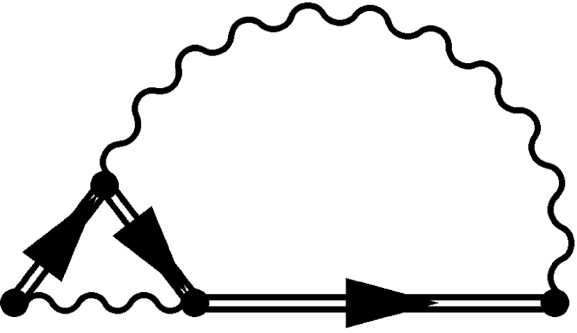
In this work we consider both first- and second-order contributions to the electron-vibron coupling. The first-order diagrams are shown in Fig. 1, and, if calculated self-consistently, equate to the commonly-used self-consistent Born approximation (SCBA). We also make use of the two second-order diagrams, those which involve two phonon excitations (Fig. 2). The first of these is similar in structure to the skeleton for electron-electron interactions, and consists of a Fock-like diagram where the phonon is dressed by a single electron-hole bubble (hence the appellation DPH for dressed-phonon diagram, Fig. 2 left). The second, which we call the double-exchange (DX) diagram (Fig. 2 right), includes two phonons simultaneously, with the second being emitted before the first is reabsorbed. The DX diagram is part of the skeleton diagrams corresponding to vertex corrections. We use these diagrams to construct expressions for the electron-vibron self-energy Dash et al. (2010) as the (total or partial) sum of each diagram: .
Note that in order to handle numerically sharply peaked functions or strongly discontinuous functions, we have found it necessary to include a very small but finite imaginary part in our expression for the bare vibron Green’s function Dash et al. (2010). This also allows us to perform calculations with a smaller number of -grid points, as long as our imaginary part in the bare vibron Green’s function is around two to three times the -grid spacing. We have already discussed in detail the effects of the corresponding extra broadening on the lineshape of the spectral functions and on the values of the linear conductance in Ref. [Dash et al., 2010].
III Results
In this section we present the effects of the second-order diagrams on the full non-equilibrium transport properties of the nanojunction in the presence of electron-vibron coupling. Calculations of the Green’s functions are performed with different levels of approximation for the electron-vibron self-energies (Figs. 1 and 2). Fully self-consistent calculations using the first-order diagrams are annotated SCBA, those using one or both second-order diagrams are annotated SC(BA+DX), SC(BA+DPH) or SC(BA+DX+DPH) as appropriate. In addition we have performed non-self-consistent second-order corrections, i.e. by using the SCBA Green’s functions to calculate the second-order diagrams, we then determine the new Green’s functions without full self-consistency. These calculations are annotated SCBA+DX or SCBA+DPH.
The inelastic properties of the system are present in the current but are better represented by the second derivative of the current as it is the signal that is directly measured experimentally in the form of the inelastic electron tunneling spectrum (IETS)Hipps and Mazur (1993).
The IETS curves present features, peaks or dips Galperin et al. (2004b); Ness et al. (2010) at biases corresponding to the energy of a specific excitation, in our case to the energy of one or several excitations of the vibration mode. The peak feature is commonly associated with the opening of a new inelastic channel for the conductance of nanojunctions in the off-resonant regime, i.e. when the electronic level is sufficiently far from the equilibrium Fermi level. In the case of the resonant transport regime (when is close to ), a dip feature is obtained in the IETS. It is associated with electron-vibron backscattering effects and a decrease in the conductance at the threshold bias. Furthermore, being the derivative of the conductance, the IETS curves also present features at biases corresponding to peaks in the conductance. We have found Dash et al. (2010) that in order to get a better aspect ratio for the IETS features corresponding to vibron excitations, it is more convenient to normalize the IETS curves by the dynamical conductance, i.e. as in Refs. Hipps and Mazur, 1993; Kushmerick et al., 2004; Yu et al., 2004, 2006; Beebe et al., 2007; Okabayashi et al., 2008; Kim et al., .
We divide our results into two sections; the first for purely inelastic features, and the second for inelastic features associated with the electron resonance effects. The first category corresponds to features observed in the IETS signal at bias equal to an integer multiple of the vibron energy , i.e. a tunneling electron excites vibrons. The second category corresponds to inelastic resonant tunneling via the vibron replica associated with the main electronic resonance at , and hence are observed in the IETS signal for biases . We will see below that the second-order diagrams have different effects on the IETS features depending upon their correspondence to one of these two categories.
III.1 Purely inelastic features
We consider first of all the off-resonant regime. In this limit the IETS features associated with inelastic resonant tunneling are sufficiently far (or sufficiently small for the higher vibron replica) from the inelastic feature at . We can thus avoid a superposition of the two different kinds of features.
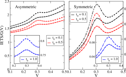
Results are presented in Fig. 3 for different electron-vibron couplings and for both symmetric and asymmetric potential drops. We note that, as would be expected intuitively, the size of the feature increases with the electron-phonon coupling —in fact the height with respect to the baseline is proportional to . As is increased, the IETS signal decreases in overall magnitude, although the feature at itself remains clear (Fig. 3 inset).
In the off-resonant regime, we do not find any difference to the curves when the second-order dressed-phonon (DPH) diagram is included. Possible reasons for this are discussed in section III.2.
We also note that the results are dependent on the symmetry of the potential drops at the left and right contact. As shown in the separate panels of Fig. 3, the curves for symmetric potential drops have a much lower baseline than for the asymmetric potential drops, although the inelastic features have the same lineshape, position and magnitude (see Figs. 3, 4 and 7). This is because (for positive bias) in the asymmetric case, is rising bias while is kept fixed at its equilibrium value. Thus is approaching the electron resonance twice as fast as in the symmetric case, where rises at the same rate as falls. The symmetric case therefore contains much less effect from the tail of the main electron resonance, and allows us to further isolate the purely inelastic part of the IETS signal.
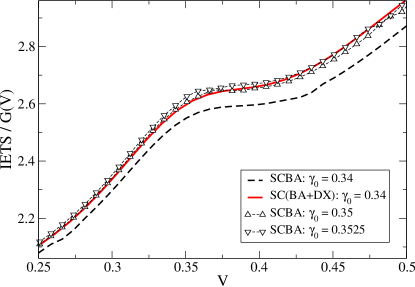
We now consider the effect of the double-exchange diagram (Fig. 2 right) on the inelastic peak at . Calculation of is extremely computationally intensive, as it can be reduced neither to a simple convolution product, nor even to a simple double-convolution product Dash et al. (2010). Calculations for the integration in the energy representation of the Green’s functions and the self-energies scale as the cube of the number of points in the energy-grid Dash et al. (2010). Moreover, as the finite imaginary part we have included in the vibron Green’s function causes extra broadening, if taken too large it washes out much of the effect of the DX diagram. In order to decrease we need to increase the number of grid points, and thus, even for our minimal model, a fully self-consistent calculation of the double-exchange diagram becomes intractable with . Hence for the DX calculations, we usually work with , giving for the total spectral width considered in our calculations.

We work around this by calculating the effects of the DX diagram both in a self-consistent manner SC(BA+DX) or non-self-consistenly as a second-order correction to the SCBA result.
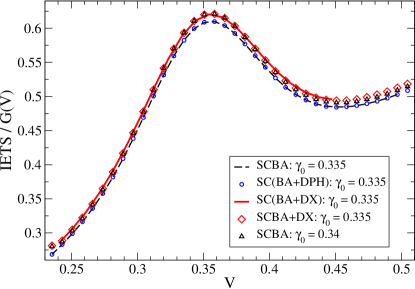
The results of this are plotted in Fig. 4. We see that the effect of the DX diagram is to both increase the height of the feature and to raise its baseline. For the set of parameters shown the self-consistency in the DX diagram calculations is not crucial.
We see that the effect of DX can also be reproduced with a SCBA calculation in which we increase the value of . Therefore the DX diagram has the effect of renormalizing as it is part of the skeleton family of vertex correction, as shown in Fig. 5. We can thus approximate the effect of the DX diagram in the IETS with a Fock-like diagram with one renormalized vertex .
The amplitude of the peak at , instead of varying as , therefore now depends on , and so we can define an effective electron-vibron coupling constant , with . This allows us to make a more quantitative analysis of by fitting the SCBA+DX curve to an SCBA curve with electron-vibron coupling , as shown in Fig. 4.
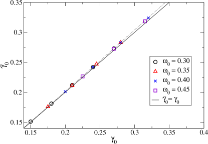
Furthermore, we can study how and are correlated by performing a series of calculations for different values of the parameters and , and then fitting the SCBA+DX results to those from SCBA calculations. The results of this are shown in Fig. 6, from which we can see that, to a first approximation, the DX diagram consistently raises the effective electron-vibron interaction by approximately 3% within the range of parameters we used.
However, we would like to point out that although the apparent effects of the DX diagram on the IETS signal is to renormalize the coupling constant , the reality is much more subtle. In Appendix A we discuss in detail the renormalization effect of the DX diagram in terms of vertex corrections, and we show that such vertex corrections do not simply correspond to a mapping of the SSSM Hamiltonian onto a similar Hamiltonian with a static renormalization of the electron-vibron coupling constant, i.e. . Rather, the vertex correction actually generates a dynamical renormalization of the electron-vibron coupling constant, i.e. .
This can be seen more clearly by considering SCBA calculations, for different values of the electron-vibron coupling parameter, and checking which of such calculations correspond the best to a SC(BA+DX) calculation. The result is shown in Fig. 7. Although the difference between the best SCBA fits and the SC(BA+DX) are not large, it is quite clear that a renormalized SCBA calculation does not provide exactly the same lineshape as a full SC(BA+DX) calculation for all the range of biases around the inelastic peak at .
Finally we expect to see a peak feature at in the IETS for the off-resonant transport regime. This peak feature is the two-vibration excitation equivalent of the feature observed at . Since this a higher-order process, the amplitude of the feature should be times smaller than the feature at . This feature has a rather small amplitude for all the electron-vibron coupling constants we have considered in this work since . An example of a close-up of the IETS feature around is given in Figure 8. We find that the amplitude of the peak with respect to the linear baseline is indeed approximately (one order of magnitude) smaller than the corresponding amplitude of the peak at (shown in Fig. 4). Once more we find that the effects of the DPH diagram are negligible for this part of the IETS signal. In Fig. 8 we also include the results of a SCBA calculation for a larger coupling which mimics the renormalization effects of the DX diagram as discussion above.
III.2 Inelastic resonant features
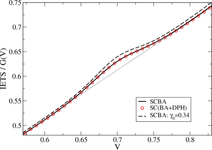
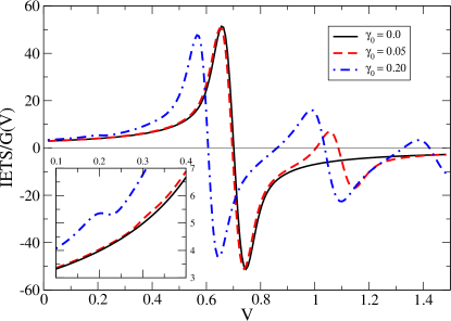
The main electron-resonance peak occurs at the polaron-shifted value of , and consists of a peak-dip feature in the IETS, as it corresponds to a resonant peak feature in the conductance. With no electron-phonon coupling (), the IETS curve has no features other than the one corresponding to the resonant transmission in the conductance at . Once the electron-phonon coupling is turned on, phonon side-band peaks emerge in the spectral function at energies . The features correspond to phonon emission (vibration excitation) by an electron, while the features correspond to phonon-emission by a hole. In the IETS, they appear as peak-dip features (derivatives of an inelastic resonant peak in the conductance) with amplitude decreasing as the bias is further increased. At lower biases however, there are no features at at the SCBA level except for very low values of the coupling to the leads (, Fig. 9 top inset).
Including the DPH diagram, however, introduces a small peak-dip features at just below the main peak-dip feature at in the IETS, as shown in Fig. 9). The DPH diagram also has a strong influence on the lineshape of the other phonon side-band peaks above , increasingly so as is brought within range of the equilibrium chemical potentials (i.e. in Fig. 9 bottom).
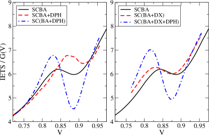
We now consider the combined effects of the DPH diagram as well as of the DX diagram on the specific case of the IETS feature at . This is shown in Figure 10. The DPH diagram increases strongly the peak-dip feature (at ) obtained from SCBA calculations at medium/strong electron-vibron coupling. Note here the importance of the self-consistency in the calculations: the second-order DPH diagram calculated as a second-order correction to SCBA (Fig. 10 left) gives a completely wrong feature in the IETS.
Interestingly, the self-consistent calculation with the DX diagram seems to give a similar feature to that observed in the SCBA calculations, but slightly shifted towards lower bias (Fig. 10 right). This is completely consistent with the renormalization effects of the electron-vibron coupling by the DX diagram as discussed in the previous section. Indeed, the DX diagram renormalizes the coupling towards a higher value . Consequently the renormalization of the molecular level by is more important than for SCBA calculations, and thus the feature is moved towards lower bias.
The calculations performed with both DX and DPH diagrams (Fig. 10 right) generate a hybrid feature in the IETS in comparison to individual calculations with the second-order diagrams. However the new IETS is not simply obtained by a linear superposition of the individual effects of the DPH and DX diagrams.
It might at first seem strange that the DPH self-energy is negligble at , where one might expect it to be influential, but that it has a significant effect at biases . While this is to some extent related to the strength of the electron-vibron coupling, there is another, more important, underlying cause. The DPH diagram involves an electron-hole bubble, and so for this diagram to become relevant, simultaneous electron and hole states must be available. This is not the case when the spectral functions of the coupled electron-vibron system are mostly empty or mostly filled. When the bias is significantly low and both Fermi levels are below the electron resonance level, these excitations are inaccessible and so there is no effects from the DPH diagram. Once the bias is increased to within range of , or however, these electron-hole states become accessible and the DPH diagram becomes influential (unless the spectral function is mostly filled). This is also borne out by the increasing contribution from DPH to the lineshape of the phonon side-band peaks as the electron level is decreased, moving DPH’s sphere of influence to lower and lower biases (see lower panel in Fig. 9).
III.3 Summary over the entire parameter range
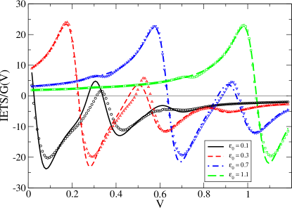
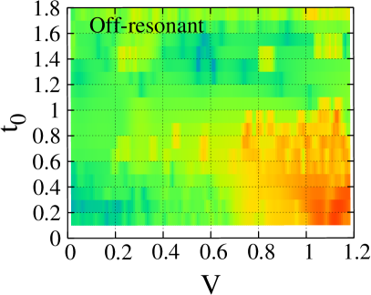
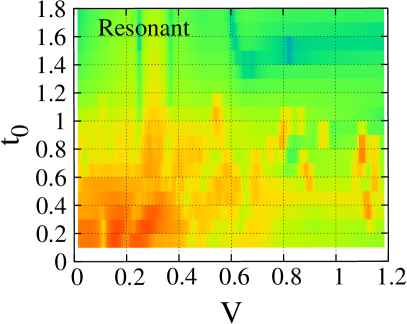
Having examined the role of the second-order diagrams in detail for characteristic selected sets of parameters, we now show results across the entire parameter range. In order to present this in a concise manner, we have compiled maps of our IETS results comparing SCBA calculations to those with SC(BA+DPH) indicating in which regimes the DPH self-energy has a significant effect. For the off-resonant regime (Fig. 11 left), we can see that the greatest effect of DPH is apparent at higher bias (i.e. approaching the electron resonance ) and when the lead-molecule-lead coupling is small. For the resonant case, however, we can see that the DPH self-energy only gives a non-negligble contribution in the region of parameter space where the coupling to the leads is small, and at low bias.
This has potential implications for real molecular junctions. Consider a junction which has its dominant molecular levels far from the equilibrium Fermi levels of the leads. At sufficiently high bias, the DPH self-energy will have a significant contribution to the inelastic spectra. This could occur in the case of a junction formed from an organic molecule if the electronic level of the molecule is within range of the intended operational bias of the junction. If however the dominant molecular electronic level is close to the leads’ Fermi levels, and the coupling to the leads is large (as would be the case, for example, in a gold nanoconstriction) then DPH will not give a significant contribution at any applied bias.
IV Conclusions
By using the non-equilibrium Green’s functions technique, we have studied the effect of electron-vibron interaction on the inelastic transport properties of single-molecule nanojunctions for a model system. We have included not only the first-order diagrams (BA) but also the second-order diagrams (double-exchange DX and dressed phonon DPH diagrams) for the electron-vibration interaction. We have calculated the inelastic electron tunneling spectrum (IETS) across the full range of parameters available to our model. The effects of the second-order DX and DPH diagrams are different and affect different features of the IETS signal. The effects of these diagrams are generally less visible in the integrated quantities, such as the current or the derivated IETS signal, than in the spectral functions Dash et al. (2010). However their effects are non-negligible, and are important for the full understanding of the spectroscopic information conveyed by the IETS signal.
The effect of the dressed-phonon (DPH) diagram is more important in the bias regions where one of the leads’ chemical potentials begins to impinge upon the electron resonance or one of its vibron replica (i.e. for resonant inelastic features). Its effect is reduced both by increasing the lead-molecule-lead coupling and/or reducing the electron-vibron interaction. The renormalization of the vibron propagator (DPH) has been shown to be strongly dependent on the self-consistency of the calculations. It would be interesting now to study the effects of the full series of the electron-hole bubble on the renormalised vibron propagator (i.e. full -like diagram).
The double-exchange diagram (DX) affects all the features in the IETS signal (i.e. resonant inelastic features and purely inelastic features at ). The corrections are small in the weak-to-medium electron-vibron coupling because they are of the order of . However we have shown, numerically and analytically, that the effect of DX is similar to a dynamical renormalization of one vertex in the Fock-like diagram. More interestingly, the complex form of the non-equilibrium dynamical renormalized electron-vibron coupling we have derived analytically can be adequately replaced in our IETS calculations by a single static renormalized parameter . This important result leads us to believe that the second-order DX calculations, which are extremely costly in computing time even for our model system, can be incorporated in calculations for realistic systems by an appropriate renormalization of the vertex in a low-computing-cost SCBA calculation.
Appendix A Non-equilibrium vertex corrections to the Fock diagram
In Appendix A of Ref.[Dash et al., 2010] we have given all the details for the derivations of the first- and second-order electron-vibron self-energies. In this section we show how the second-order double-exchange (DX) diagram can be recast in an effective first-order Fock-like diagram with a renormalized vertex.
We recall that for the SSSM model, the Fock and DX self-energies defined on the Keldysh contour are given by
| (6) |
and
| (7) |
The DX self-energy can be rewritten as an effective Fock-like diagram after introducing a renormalized electron-vibron coupling parameter and the vertex function :
| (8) |
with
| (9) |
and where the vertex function is given by
| (10) |
The above expression for the vertex function is compatible with the second-order expansion of the electron-vibron interaction. A generalization of the vertex function (see Fock-like diagram in Figure 5) to all orders of the interaction is possible, though beyond the scope of the present paper. Note that at the lowest order, the renormalized electron-vibron coupling parameter would be given by with . Hence Eq.(7) would simply be transformed Eq.(6) as expected.
Using the rules of analytical continuation on the real-time branches given in Appendix A of paper Ref.[Dash et al., 2010], we find the different components of the self-energies. Then after taking the Fourier transform of the different quantities in the steady-state limit, i.e. , we find the following expression for the different components of the energy-dependent self-energies:
| (11) |
and
| (12) |
where the non-equilibrium dynamical renormalised electron-vibron coupling is given by
| (13) |
(The index labels the branch of the Keldysh time-loop contour and are related to the usual convention: time-ordered (), anti time-ordered (), greater () and lesser () components.)
Because all the quantities are originally defined on and because the vertex function is a 3-point (3 times) function, the non-equilibrium dynamical renormalized electron-vibron coupling is a complex function of three indices and of two energy variables. Such a dynamical renormalization (including non-equilibrium conditions) is much more complicated than a simple static renormalization of the electron-vibron constant coupling .
In our analysis of the IETS signal in the off-resonant transport regime, we try to keep the interpretation of the results as simple as possible, and we show that the renormalization of the IETS signal due to the DX diagram can be fairly well approximated by a simple static renormalization of the coupling constant for applied bias around the vibration frequency .
Acknowledgements.
This work was funded in part by the European Community’s Seventh Framework Programme (FP7/2007-2013) under grant agreement no 211956 (ETSF e-I3 grant).References
- Hipps and Mazur (1993) K. W. Hipps and U. Mazur, Journal of Physical Chemistry 97, 7803 (1993).
- Liu et al. (2004) N. Liu, N. A. Pradhan, and W. Ho, Journal of Chemical Physics 120, 11371 (2004).
- Kushmerick et al. (2004) J. G. Kushmerick, J. Lazorcik, C. H. Patterson, and R. Shashidhar, Nano Letters 4, 639 (2004).
- Yu et al. (2004) L. H. Yu, Z. K. Keane, J. W. Ciszek, L. Cheng, M. P. Stewart, J. M. Tour, and D. Natelson, Physical Review Letters 93, 266802 (2004).
- Yu et al. (2006) L. H. Yu, C. D. Zangmeister, and J. G. Kushmerick, Nano Letters 6, 2515 (2006).
- Chae et al. (2006) D.-H. Chae, J. F. Berry, S. Jung, F. A. C. C. A. Murillo, and Z. Yao, Nano Letters 6, 165 (2006).
- Beebe et al. (2007) J. M. Beebe, H. J. Moore, T. R. Lee, and J. G. Kushmerick, Nano Letters 7, 1364 (2007).
- Okabayashi et al. (2008) N. Okabayashi, Y. Konda, and T. Komeda, Physical Review Letters 100, 217801 (2008).
- Gawronski et al. (2009) H. Gawronski, J. Fransson, and K. Morgenstern, Imaging of inelastic waves in iets maps (2009), eprint [arXiv]arXiv:0911.4053v1.
- (10) Y. Kim, H. Song, F. Strigl, H.-F. Pernau, and T. L. and, Mechanical control of vibrational states in single-molecule junctions, eprint [arXiv]arXiv:1011.3226v1.
- Hyldgaard et al. (1994) P. Hyldgaard, S. Hershfield, J. H. Davies, and J. W. Wilkins, Annals of Physics 236, 1 (1994).
- Ness and Fisher (1999) H. Ness and A. J. Fisher, Physical Review Letters 83, 452 (1999).
- Ness et al. (2001) H. Ness, S. A. Shevlin, and A. J. Fisher, Physical Review B 63, 125422 (2001).
- Ness and Fisher (2002) H. Ness and A. J. Fisher, Europhysics Letters 57, 885 (2002).
- Flensberg (2003) K. Flensberg, Physical Review B 68, 205323 (2003).
- Mii et al. (2003) T. Mii, S. Tikhodeev, and H. Ueba, Physical Review B 68, 205406 (2003).
- Montgomery et al. (2003) M. J. Montgomery, J. Hoekstra, A. P. Sutton, and T. N. Todorov, Journal of Physics: Condensed Matter 15, 731 (2003).
- Troisi et al. (2003) A. Troisi, M. A. Ratner, and A. Nitzan, Journal of Chemical Physics 118, 6072 (2003).
- Chen et al. (2005a) Y. C. Chen, M. Zwolak, and M. di Ventra, Nano Letters 4, 1709 (2005a).
- Lorente and Persson (2000) N. Lorente and M. Persson, Physical Review Letters 85, 2997 (2000).
- Frederiksen et al. (2004) T. Frederiksen, M. Brandbyge, N. Lorente, and A. P. Jauho, Physical Review Letters 93, 256601 (2004).
- Galperin et al. (2004a) M. Galperin, M. A. Ratner, and A. Nitzan, Nano Letters 4, 1605 (2004a).
- Galperin et al. (2004b) M. Galperin, M. A. Ratner, and A. Nitzan, Journal of Chemical Physics 121, 11965 (2004b).
- Mitra et al. (2004) A. Mitra, I. Aleiner, and A. J. Millis, Physical Review B 69, 245302 (2004).
- Pecchia et al. (2004) A. Pecchia, A. di Carlo, A. Gagliardi, S. Sanna, T. Frauenhein, and R. Gutierrez, Nano Letters 4, 2109 (2004).
- Pecchia and di Carlo (2004) A. Pecchia and A. di Carlo, Reports on Progress in Physics 67, 1497 (2004).
- Chen et al. (2005b) Z. Chen, R. Lü, and B. Zhu, Physical Review B 71, 165324 (2005b).
- Paulsson et al. (2005) M. Paulsson, T. Frederiksen, and M. Brandbyge, Physical Review B 72, 201101 (2005).
- Ryndyk and Keller (2005) D. A. Ryndyk and J. Keller, Physical Review B 71, 073305 (2005).
- Sergueev et al. (2005) N. Sergueev, D. Roubtsov, and H. Guo, Physical Review Letters 95, 146803 (2005).
- Viljas et al. (2005) J. K. Viljas, J. C. Cuevas, F. Pauly, and M. Häfner, Physical Review B 72, 245415 (2005).
- Yamamoto et al. (2005) T. Yamamoto, K. Watanabe, and S. Watanabe, Physical Review Letters 95, 065501 (2005).
- Cresti et al. (2006) A. Cresti, G. Grosso, and G. P. Parravicini, Journal of Physics: Condensed Matter 18, 10059 (2006).
- Kula et al. (2006) M. Kula, J. Jiang, and Y. Luo, Nano Letters 6, 1693 (2006).
- Paulsson et al. (2006) M. Paulsson, T. Frederiksen, and M. Brandbyge, Nano Letters 6, 258 (2006).
- Ryndyk et al. (2006) D. A. Ryndyk, M. Hartung, and G. Cuniberti, Physical Review B 73, 045420 (2006).
- Troisi and Ratner (2006) A. Troisi and M. A. Ratner, Nano Letters 6, 1784 (2006).
- de la Vega et al. (2006) L. de la Vega, A. Martín-Rodero, N. Agraït, and A. Levy-Yeyati, Physical Review B 73, 075428 (2006).
- Toroker and Peskin (2007) M. C. Toroker and U. Peskin, Journal of Chemical Physics 127, 154706 (2007).
- Frederiksen et al. (2007) T. Frederiksen, M. Paulsson, M. Brandbyge, and A.-P. Jauho, Physical Review B 75, 205413 (2007).
- Galperin et al. (2007) M. Galperin, A. Nitzan, and M. A. Ratner, Physical Review B 74, 075326 (2007).
- Ryndyk and Cuniberti (2007) D. A. Ryndyk and G. Cuniberti, Physical Review B 76, 155430 (2007).
- Schmidt et al. (2007) B. B. Schmidt, M. H. Hettler, and G. Schön, Physical Review B 75, 115125 (2007).
- Troisi et al. (2007) A. Troisi, J. M. Beebe, L. B. Picraux, R. D. van Zee, D. R. Stewart, M. A. Ratner, and J. G. Kushmerick, Proceedings of the National Academy of Sciences of the USA 104, 14255 (2007).
- Asai (2008) Y. Asai, Physical Review B 78, 045434 (2008).
- Benesch et al. (2008) C. Benesch, M. Čížek, J. Klimeš, I. Kondov, M. Thoss, and W. Domcke, Journal of Physical Chemistry C 112, 9880 (2008).
- Paulsson et al. (2008) M. Paulsson, T. Frederiksen, H. Ueba, N. Lorente, and M. Brandbyge, Physical Review Letters 100, 226604 (2008).
- Egger and Gogolin (2008) R. Egger and A. O. Gogolin, Physical Review B 77, 113405 (2008).
- Monturet and Lorente (2008) S. Monturet and N. Lorente, Physical Review B 78, 035445 (2008).
- McEniry et al. (2008) E. J. McEniry, T. Frederiksen, T. N. Todorov, D. Dundas, and A. P. Horsfield, Physical Review B 78, 035446 (2008).
- Ryndyk et al. (2009) D. A. Ryndyk, R. Gutiérrez, B. Song, and G. Cuniberti, in Energy Transfer Dynamics in Biomaterial Systems, edited by I. Burghardt, V. May, D. A. Micha, and E. R. Bittner (Springer Berlin Heidelberg, 2009), vol. 93 of Springer Series in Chemical Physics, pp. 213–335, ISBN 978-3-642-02306-4.
- Schmidt et al. (2008) B. B. Schmidt, M. H. Hettler, and G. Schön, Physical Review B (Condensed Matter and Materials Physics) 77, 165337 (2008).
- Tsukada and Mitsutake (2009) M. Tsukada and K. Mitsutake, Journal of the Physical Society of Japan 78, 084701 (2009).
- Loos et al. (2009) J. Loos, T. Koch, A. Alvermann, A. R. Bishop, and H. Fehske, Journal of Physics: Condensed Matter 21, 395601 (2009).
- Avriller and Yeyati (2009) R. Avriller and A. L. Yeyati, Physical Review B 80, 041309 (2009).
- Haupt et al. (2009) F. Haupt, T. Novotný, and W. Belzig, Phys. Rev. Lett. 103, 136601 (2009).
- Dash et al. (2010) L. K. Dash, H. Ness, and R. W. Godby, Journal of Chemical Physics 132, 104113 (2010).
- Ness et al. (2010) H. Ness, L. Dash, and R. W. Godby, Physical Review B 82, 085426 (2010).
- Wang and Thoss (2011) H. Wang and M. Thoss, Numerically exact, time-dependent treatment of vibrationally coupled electron transport in single-molecule junctions (2011), eprint [arXiv]arXiv:1103.4945v1.
- Garcia-Lekue et al. (2011) A. Garcia-Lekue, D. Sanchez-Portal, A. Arnau, and T. Frederiksen, Simulation of inelastic electron tunneling spectroscopy of single molecules with functionalized tips (2011), eprint [arXiv]arXiv:1103.4302v1.
- Ueda et al. (2011) A. Ueda, O. Entin-Wohlman, and A. Aharony, Effects of coupling to vibrational modes on the ac conductance of molecular junctions (2011), eprint [arXiv]arXiv:1101.4440v1.
- Meir and Wingreen (1992) Y. Meir and N. S. Wingreen, Physical Review Letters 68, 2512 (1992).
- Datta et al. (1997) S. Datta, W. D. Tian, S. H. Hong, R. Reifenberger, J. I. Henderson, and C. P. Kubiak, Physical Review Letters 79, 2530 (1997).