Terahertz radiation driven chiral edge currents in graphene
Abstract
We observe photocurrents induced in single layer graphene samples by illumination of the graphene edges with circularly polarized terahertz radiation at normal incidence. The photocurrent flows along the sample edges and forms a vortex. Its winding direction reverses by switching the light helicity from left- to right-handed. We demonstrate that the photocurrent stems from the sample edges, which reduce the spatial symmetry and result in an asymmetric scattering of carriers driven by the radiation electric field. The developed theory is in a good agreement with the experiment. We show that the edge photocurrents can be applied for determination of the conductivity type and the momentum scattering time of the charge carriers in the graphene edge vicinity.
pacs:
73.50.Pz, 72.80.Vp, 81.05.ue, 78.67.WjThe “bulk” transport properties of graphene have been studied intensively in recent years and yielded insight into the half-integer and fractional quantum Hall effect, phase-coherent effects or spin transport on the micrometer scale, to name a few examples Bib:Novoselov2004 ; sarma . While the details of each of those effects depend crucially on the linear dispersion relation of graphene and its specific material properties, most of the transport phenomena have already been studied in other two-dimensional systems. Graphene edges, on the other hand, were predicted to show insulating or metallic, even magnetic behavior, depending on the crystallographic orientation and edge chemistry. In scanning tunneling experiments, an enhanced edge density of states was shown Tun2 ; Tun4 and Raman scattering experiments provided evidence for the dependence of scattering mechanisms on the edge orientation Raman1 ; Raman3 . In transport experiments edge effects are usually masked by bulk properties, nonetheless the graphene edges are expected to play a crucial role in the electronic properties of graphene-based nanoscale devices.
Here, we present an opto-electronic method to uniquely distinguish edge from bulk scattering by exploring edge photocurrents in graphene samples illuminated by terahertz (THz) radiation. For circularly polarized light the edge current is observed to form a vortex winding around the edges of the square-shaped samples. Its direction reverses upon switching the radiation helicity from left- to right-handed. Evidently, the photocurrent is caused by the local symmetry breaking at the sample edges resulting in an asymmetric scattering of carriers driven by the radiation electric field. It gives rise to a directed electric current along the sample boundary in a narrow stripe of width comparable to the mean free path. We show that the photocurrent measurements provide direct access to electron scattering at the graphene edges and allow to map the variation of scattering times along the edges.
We investigated two types of single-layer graphene samples: (i) large-area epitaxial graphene prepared by high-temperature Si sublimation of 4H and 6H polytypes of semi-insulating SiC substrates erl1 ; LaraAvival09 ; erl2 and (ii) small area exfoliated graphene flakes Bib:Novoselov2004 deposited on oxidized silicon wafers. Below, we report results on epitaxial graphene samples (labeled #1-4H, #2-4H, and #3-6H) and three samples prepared from exfoliated graphene. Hall measurements indicate that the epitaxial samples are -doped (due to charge transfer from SiC erl1 ) while the exfoliated samples are -doped. The measured carrier density lies in the range 1012 cm-2, the Fermi energy ranges from 200 to 300 meV and the mobility is about 1000 cm2/Vs at room temperature. Ohmic contacts were made at samples’ edges (see, e.g., inset of Fig. 1). Details on the material growth and characterization can be found in Suppl .
The experiments on edge photocurrents are performed applying alternating electric THz fields of a high power pulsed NH3 laser JETP1982 ; laser2 ; Ganichevbook operating at wavelengths m, m or 280 m (frequencies THz, 2 THz and 1.1 THz, respectively). The radiation induces indirect (Drude-like) optical transitions, because the photon energies are much smaller than the carrier Fermi energy. The NH3 laser generates single pulses with a duration of about 100 ns, peak power of 10 kW, and a repetition rate of 1 Hz. A typical spot diameter from 1 to 3 mm. The beam has an almost Gaussian form, which is measured by a pyroelectric camera ch1Ziemann2000p3843 .
All experiments are performed at normal incidence of light and at room temperature. Elliptically and, in particular, circularly polarized radiation is obtained applying /4 quartz plates. The resulting polarization state described by the Stokes parameters Stokes , , and is directly related to the angle between the initial linear polarization of the laser light along the -axis and the plate optical axis. The experimental geometry is shown in Figs. 1, 2, and 3. The current is measured via the voltage drop across a 50 load resistor.
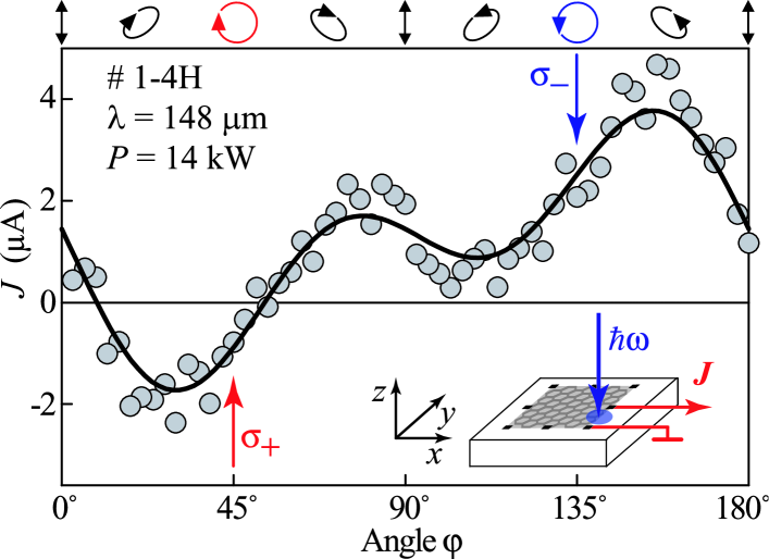
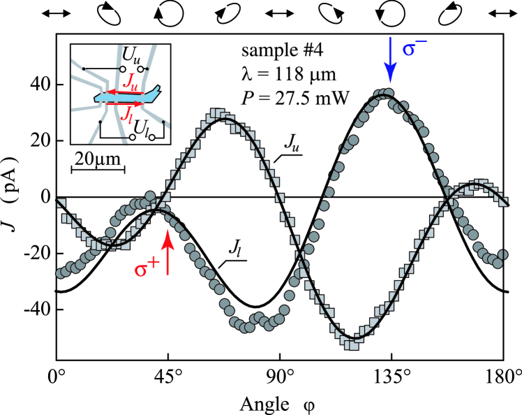
Illumination of the edge of unbiased large-area samples between any pair of contacts results in a photocurrent. By contrast, if the laser spot is moved toward the center the signal vanishes. The detected signal depends strongly on the radiation polarization, Fig. 1. The principal observation is that for right- () and left-handed () polarizations, i.e., for and 135∘, the signs of the photocurrent are opposite. The overall dependence is more complex. It is well described by
| (1) | |||||
and corresponds to the superposition of the Stokes parameters with different weights. The first term given by the coefficient is just proportional to the radiation helicity, whereas the second () and third () terms change with degree and orientation of the linear polarization. Note that the observed offset is usually smaller or comparable to , , and (see Fig. 1). In our present study we focus on the helicity driven photocurrent . This is the only contribution which reverses the current direction upon switching the radiation helicity from to . We also note that, for circularly polarized light ( and ) and , the current is solely determined by the first term in Eq. (1). Therefore, it would be sufficient to measure the response to circularly polarized radiation. However, to increase the accuracy, we always measured the whole polarization dependence, like the one shown in Fig. 1, and extracted by fitting Eq. (1) to the data.
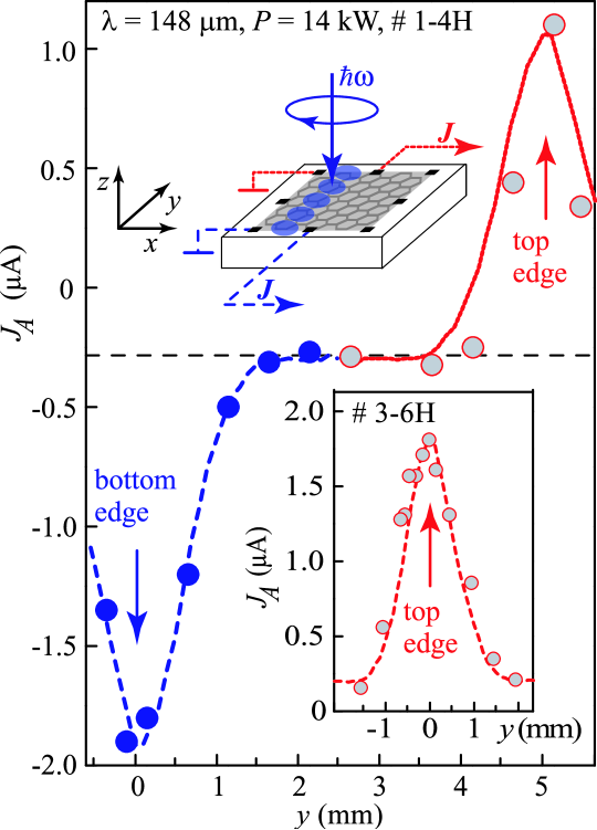
To prove that the photocurrent is caused by illuminating the graphene edges, we scanned the laser spot across the sample along the -axis. The signal was picked up from a pair of contacts at the sample top and bottom edges aligned along the -axis. The experimental geometry and the photocurrent versus the spot position are shown in Fig. 2. The current reaches its maximum for the laser spot centered at the edge and rapidly decays with the spot moving. Comparison of with the independently recorded laser profile (dotted line) shows that the signal just follows the Gaussian intensity profile. This observation unambiguously demonstrates that the photocurrent is caused by illuminating the sample edges. Moreover, Fig. 2 reveals that the helicity driven current changes its sign for opposite edges.
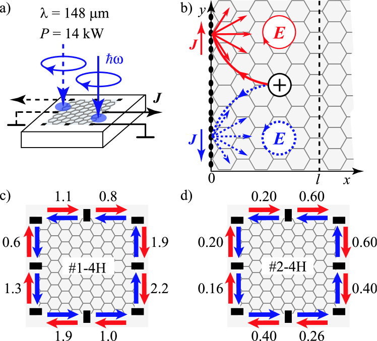
The above results show that the current direction at a specific edge depends on the light helicity. To check this in more detail, we investigated currents excited by circularly polarized radiation for different pairs of contacts. Here, the laser spot is always centered between the contacts, see Fig. 3a. The current direction for (red arrows) and (blue arrows) circularly polarized radiation and the magnitude of for various contact pairs are shown in Fig. 3b and 3c. The figures document a remarkable behavior of the circular edge photocurrent: it forms a vortex winding around the edges of the square shaped samples which reverses its direction upon switching from right- to left-handed. These dependencies are observed for all used wavelengths and samples. Helicity driven currents have also been observed for small area graphene flakes, see Suppl for details.
The observation that a photocurrent occurs only if the laser spot is adjusted to an edge agrees with the symmetry analysis: In the ideal honeycomb lattice of graphene and for our experimental geometry, any photoelectric effect is forbidden PRL10 , because the two-dimensional structure of graphene possesses a center of space inversion. Thus, the appearance of photocurrents at normal incidence of radiation is a clear manifestation of the symmetry reduction of the system, in our case, due to the edges. We also note that the typical photon energy 10 meV used in experiment is much smaller than the characteristic energy of carriers meV. Thus, the mechanism of current formation can be treated classically and should involve the action of the light’s electric field on free carriers in the vicinity of a graphene edge.
A microscopic process actuating the edge photocurrent generation is illustrated in Fig. 3b. It involves the time dependent motion of carriers under the action of the electric field of circularly polarized radiation and scattering at the sample edge. We note that this mechanism is similar to that of the surface photogalvanic effect observed in bulk materials Magarill ; Alperovich . The microscopic theory of edge currents is developed in the framework of the Boltzmann kinetic equation. In this approach, the electron (hole) distribution is described by the function . It depends on the carrier momentum , coordinate ( for a semi-infinite layer), time , and obeys the equation
| (2) |
where is the electric field of the radiation, is the electron velocity, m/s is the effective speed, is the carrier charge ( for holes and for electrons), and is the collision integral. The distribution function can be expanded in series of powers of the electric field,
| (3) |
where is the equilibrium distribution function with being the electron energy, , and . The first order in correction to the distribution function oscillates with frequency and does not contribute to a current. The directed electric current along the structure edge is, therefore, determined by the second order E-field correction and given by
| (4) |
The factor 4 accounts for the spin and valley degeneracy.
We solve Eq. (2) and calculate the current, Eq. (4), for the simple form of the collision integral,
| (5) |
with being the scattering time, and the boundary condition at ,
| (6) |
corresponding to diffusive scattering. In the case of a degenerate gas, the edge current takes the form (see Suppl for details):
| (7) |
The helicity-driven current is given by the first term because for our geometry where the light propagates along . The second term yields the current caused by linearly polarized radiation and vanishes for circular polarization. In the case of elliptically polarized light, . Both contributions are clearly detected in the experiment and correspond to the first () and second () terms in the empirical Eq. (1), see Fig. 1.
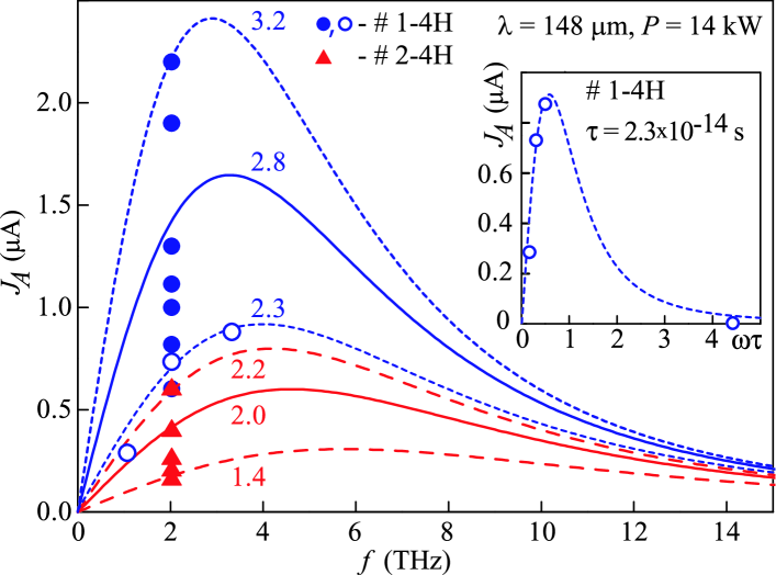
The helicity driven photocurrent described by Eq. (7) vanishes for zero frequency, has a maximum at and decreases rapidly at higher frequencies. Exactly this behavior is found in experiment (see inset of Fig. 4) as we explain in more detail below. The only free parameter in Eq. (7) is the scattering time . Corresponding data are shown in Fig. 3 where the photocurrent values measured at 2 THz for each of the contact pairs are plotted. These data points are first compared to calculated traces of employing Eq. (7). Solid lines are calculated using the bulk values for the time extracted from resistivity and carrier density for samples #1-4H ( s) and #2-4H ( s). The bulk scattering times used in Eq. (7) give for some of the contact pairs already perfect quantitative agreement. For other edge segments the current deviates significantly. This is a consequence of the strongly non-linear dependence of on . Varying by only 15% changes the current by %. By fitting the photocurrent we can extract the local scattering time for every edge segment shown in Figs. 3c and d). The best fits are shown by dashed lines in Fig. 4 and constitute a map of scattering times along the edge. The average value of the circular edge current scales with the sample mobility. To check the frequency dependence predicted by Eq. (7) we show in the inset of Fig. 4 vs. for one edge segment using the extracted . The data points are perfectly described by Eq. (7) and confirm the model.
While the magnitude of the circular edge photocurrent agrees well with theory, the expected polarity of for -type graphene is opposite to the one observed. This, at first glance, surprising result agrees with results from spatially resolved Raman measurements demonstrating that edges of -type graphene layers exhibit -type conductivity Raman1 ; Raman3 . This explains the sign of the photocurrent, which is generated in a narrow edge channel comparable to the mean free path ( nm) and has opposite sign for electrons and holes, see Eq. (7). Actually, the difference in the conductivity type can be also understood from the details of the sample fabrication. It is well established that epitaxial graphene on SiC(0001) is -doped due to charge transfer from the interfacial buffer layer (see, e.g., erl1 ; LaraAvival09 ), while so-called quasi-free-standing graphene, lacking such buffer layer and sitting on a hydrogen terminated SiC(0001) surface, is -doped erl5 . Therefore, it is reasonable that the edges of epitaxial graphene, exposed to the SiC substrate without the interfacial layer, can be -doped. This assumption is corroborated by similar reports on the transition from - to -type of doping at the edges of graphene flakes on SiO2, which were attributed to the difference in the work functions of graphene and the substrate SK_TS4 .
To summarize, our observations clearly demonstrate that illuminating monolayer graphene edges with polarized terahertz radiation at normal incidence results in a directed electric edge current. The effect is directly coupled to electron scattering at the graphene edge and vanishes in bulk graphene. Our results suggest that circular the photocurrents can be effectively used to study edge transport in graphene even at room temperature.
We thank K. S. Novoselov, V. Lechner, S. Heydrich and V. V. Bel’kov for fruitful discussions. Support from DFG (SPP 1459 and GRK 1570), EU-ConceptGraphene, Linkage Grant of IB of BMBF at DLR, RFBR, Russian Ministry of Education and Sciences, and “Dynasty” Foundation–ICFPM is acknowledged.
I Supplemental Material
I.1 S1. Details of the Samples
We investigated three epitaxial samples grown on SiC. Samples #1-4H and #2-4H were grown by the Linköping group on a Si-terminated surface of a 4H-SiC(0001) semi-insulating substrate (Cree Inc.) LaraAvival09 . The reaction kinetics on the Si-terminated surface is slower than on the C-face because of the higher surface energy, which fosters homogeneous and well controlled graphene formation erl1 . Graphene was grown at a temperature of 2000∘C and 1 atm Ar gas pressure resulting in monolayers of graphene atomically uniform over more than 1000 m2, as shown by low-energy electron microscopy Virojanadara08 . Eight contacts were produced by depositing 3 nm of Ti and 100 nm of Au. The quadratic sample size of mm2 was achieved by oxygen plasma etching of all four edges. Hall measurements indicate that the large area samples are -doped due to charge transfer from SiC LaraAvival09 ; erl1 ; Bostwick09 ; SK_TS1a ; SK_TS1b ; SK_TS2 . The measured carrier concentration is between 1012 cm-2 and 1012 cm-2, the Fermi energy ranges from 200 to 300 meV and the mobility is about 1000 cm2/Vs at room temperature. In these samples, as well as in other large-area samples, the resistance at room temperature is about 2 to 5 k.
The third epitaxial graphene sample #3-6H, was grown by the Erlangen group on 6H-SiC(0001) wafers (II-VI Inc.). Graphene growth was performed using sublimation growth in Ar atmosphere erl1 ; erl2 . First, polishing damage was removed by etching the substrate in 1 bar hydrogen at 1550∘C for 15 min. Second, graphene was grown by annealing the sample in 1 bar Ar at a temperature of 1650∘C for 15 min. The graphene coverage was determined by x-ray photoelectron spectroscopy (XPS). The square-shaped sample size of mm2 was achieved by mechanical cutting the edges. Both, carrier density and mobility in the -type sample #3-6H are very similar to those of the Linköping samples.
For all epitaxial graphene samples, low-temperature quantum Hall measurements reveal the high quality and homogeneity.
The exfoliated graphene samples (small-area graphene samples 4, 5, and 6) has been prepared from natural graphite using the mechanical exfoliation technique Bib:Novoselov2004 on an oxidized silicon wafer. The oxide thickness of nm allowed to locate graphene flakes in an optical microscope and to assess their thickness. We checked the reliability of this method using Raman spectroscopy and low-temperature quantum Hall measurements on similar samples jonathan1 . The single layer graphene flakes obtained by this method were typically -doped by adsorbed contaminants with carrier concentrations cm-2. The Fermi energies were meV and the mobilities at room temperature of the order of cm2/Vs. The flakes included in this study were all single layer with the flakes size of the order of 10 to 30 micrometers. The sample morphology was characterized by atomic force microscopy measurements under ambient conditions with the microscope in intermittent contact mode with standard silicon tips jonathan2 . After recording the position of the flakes with respect to predefined markers, we contacted them by electron beam lithography and thermal evaporation of 60 nm Pd electrodes. The resistance of graphene measured between various contacts was about 1 to 3 k.
I.2 S2. Laser beam parameters
In addition to the pulsed THz laser described in the main text, we also used a continuous-wave (cw) CH3OH laser (m) with a power of 20 mW. In the experiments applying the CH3OH laser, the cw radiation was modulated at chopper frequencies in the range from to Hz. The sign of the signal is defined as a relative phase with respect to the lock-in reference signal, which was kept the same for all measurements.
Elliptically and, in particular, circularly polarized radiation has been obtained by transmitting the laser beam, which is initially linearly polarized along the -direction for the pulsed laser and along the -direction for the cw laser, through /4 crystal quartz plates. The resulting polarization state is directly related to the angle between the initial linear polarization of the laser light and the optical axis of the plate. It is described by the Stokes parameters Stokes . In particular, the dependence of the circular polarization degree, given by , on the angle in our experimental geometry has the form
| (8) |
The parameters and are given by the bilinear combinations of the polarization vector components,
| (9) | |||
The parameters and describe the degree of linear polarization in the coordinate axes and in the coordinate frame rotated about an angle of 45∘, respectively Stokes . Note that radiation is incident along axis. The resulting polarization ellipses for the cw THz laser for some angles are sketched on top of Fig. 5. Further details on the experimental technique can be found in Ref. GaN2008 .
I.3 S3. Photocurrents in small-area samples
Helicity driven photocurrents excited at normal incidence have also been observed in small-area graphene flakes. Examples of the current polarization dependence are shown in Fig. 5 for two different pairs of contacts. Similar to data obtained in large-area samples, it can be well fitted by Eq. (1) of the main text, which reads
| (10) |
While photocurrents are observed in both large-area and small-area samples, the analysis of the edge photocurrents is much easier in the large-area samples. Actually only in the latter type of samples the illumination of a single edge by THz radiation could be realized in our experiments. Such selective excitation has enabled the accurate analyses of the edge currents. By contrast, in micron-sized exfoliated samples the spot size is much larger than the graphene flakes and the effects of different edges are superimposed.
I.4 S4. Theory
Equation (7) of the main text is obtained by expanding the distribution function in series of the electric field. To first order in the electric field, solution of Eq. (2) with the boundary condition (6) has the form
| (11) |
where . The equation for the second-order correction is given by
| (12) |
which yields
| (13) |
By using Eq. (4) for the edge electric current and Eq. (13) we derive
| (14) |
where the above two contributions to the current stem from the first and second terms on the right-hand side of Eq. (13), respectively. Finally, taking into account that the electron energy and velocity in graphene are given by and , respectively, and assuming that the electron gas is degenerate and is independent of , we obtain Eq. (7) of the main text.
The current Eq. (7) of the main text is consistent with the point-group symmetry Cs containing the mirror plane . It should be noted that for elliptical polarization, in some experiments the photocurrent described by Eq. (7) is superimposed with an additional contribution proportional to [see the third term in Eq. (10)]. This term can be attributed to a lowering of the system symmetry to C1 showing the non-equivalence of and directions, e.g., due to (i) inhomogeneous photoexcitation, (ii) macroscopic roughness of the investigated edges, (iii) non-equivalence of contacts, etc. The symmetry reduction hinders the edge photogalvanic currents under study and complicates their analysis. However, the obstacle can be easily overcome applying circularly polarized radiation, like used in the present work. Indeed, as addressed above the edge currents driven by circularly polarized light change their signs upon variation of the radiation helicity. By contrast, other current contributions caused by the additional symmetry lowering are insensitive to the radiation helicity and vanish for circularly polarized radiation.
References
- (1) K. S. Novoselov et al., Science 306, 666 (2004).
- (2) S. Das Sarma et al., Rev. Mod. Phys. 83, 407 (2011).
- (3) Y. Nimi, et al. Phys. Rev. B 73, 085421 (2006).
- (4) K. A. Ritter and J. W. Lyding Nature Mat. 8, 235 (2009).
- (5) C. Casiraghi et al., Nano Lett. 9, 1433 (2009).
- (6) S. Heydrich et al., Appl. Phys. Lett. 97, 043113 (2010).
- (7) K. V. Emtsev et al., Nature Mat. 8, 203 (2009).
- (8) A. Tzalenchuk et al., Nature Nanotech. 5, 186 (2010).
- (9) M. Ostler et al., Phys. Stat. Sol. B 247, 2924 (2010).
- (10) See Supplemental Material.
- (11) S. D. Ganichev, S. A. Emel’yanov, and I. D. Yaroshetskii, JETP Lett. 35, 368 (1982).
- (12) S. D. Ganichev et al., Phys. Rev. Lett. 80, 2409 (1998).
- (13) S. D. Ganichev and W. Prettl, Intense Terahertz Excitation of Semiconductors (Oxford Univ. Press, 2006).
- (14) E. Ziemann et al., J. Appl. Phys. 87, 3843 (2000).
- (15) B. E. A. Saleh and M. C. Teich, Fundamentals of Photonics (John Wiley & Sons, Inc., 2007).
- (16) J. Karch et al., Phys. Rev. Lett. 97, 182107 (2010).
- (17) L. I. Magarill and M. V. Entin, Phys. Solid State 21, 743 (1979).
- (18) V. L. Alperovich et al., JETP Lett. 31, 547 (1980).
- (19) F. Speck et al., arXiv:1103.399v1.
- (20) E. J. H Lee et al., Nature Nano. 3, 486 (2008).
- (21) C. Virojanadara et al., Phys. Rev. B 78, 245403 (2008).
- (22) A. Bostwick et al., Nature Phys. 3, 36 (2007).
- (23) T. Ohta et al., Phys. Rev. Lett. 98 206802 (2007).
- (24) K. V. Emtsev et al., Phys. Rev. B. 77, 155303 (2008).
- (25) S. Kopylov et al., Appl. Phys. Lett. 97, 112109 (2010).
- (26) J. Eroms and D. Weiss, New J. Phys. 11, 095021 (2009).
- (27) U. Stöberl et al., Appl. Phys. Lett. 93, 051906 (2008).
- (28) W. Weber et al., Phys. Rev. B 77, 245304 (2008).