Drift velocity peak and negative differential mobility in high field transport in graphene nanoribbons explained by numerical simulations
Abstract
We present numerical simulations of high field transport in both suspended and deposited armchair graphene nanoribbon (A-GNR) on HfO2 substrate. Drift velocity in suspended GNR does not saturate at high electric field (), but rather decreases, showing a maximum for kV/cm. Deposition on HfO2 strongly degrades the drift velocity by up to a factor of with respect to suspended GNRs in the low-field regime, whereas at high fields drift velocity approaches the intrinsic value expected in suspended GNRs. Even in the assumption of perfect edges, the obtained mobility is far behind what expected in two-dimensional graphene, and is further reduced by surface optical phonons.
pacs:
73.63.-b,73.50.Dn,72.80.Vp,63.22.-mAssessing the potential of Graphene Nanoribbons (GNRs) for future electronic applications requires full understanding of both quasi-equilibrium and far-from-equilibrium transport mechanisms Wang et al. (2008); Betti et al. (2011). However experimental low-field (LF) mobility in 1 nm-wide GNRs can be as low as 100 cm2/Vs and is limited by edge disorder Wang et al. (2008); Yang and Murali (2010). Furthermore, we know that achieving ideally smooth edges is not enough: full-band (FB) modeling shows that LF mobility due to only acoustic (AC) phonon scattering at low fields is close to 500 cm2/Vs for 1 nm-wide GNRs Betti et al. (2011a). Most importantly, nanoscale transistors do not operate in the LF mobility limit. Therefore, simulation of far-from-the-equilibrium transport conditions is required to understand achievable device performance. Whereas at low field carrier scattering is mainly due to low-energy intravalley acoustic phonons Betti et al. (2011a), at high electric field scattering is dominated by optical phonon emission (EM), which becomes relevant when electrons gain enough energy to emit optical phonons. High-field steady-state transport can be simulated by solving the Boltzmann transport equation (BTE) through the single-particle Monte Carlo (MC) method. When dealing with 1D systems, however, particular attention has to be paid in accurately describing the energy dispersion relation due to quantum lateral confinement: for each GNR subband there is a parabolic behavior close the subband minimum, and then the typical graphene quasi-linear behavior already for relatively small wavevector values, corresponding to a velocity m/s. Some authors have considered phonon confinement and multisubband transport, focusing on quantum wires with the effective mass approximation Briggs and Leburton (1988); Mickevicius et al. (1992). For GNRs, a multisubband MC approach has been followed in Zeng et al. (2009) and BTE has been solved in a deterministic way at criogenic temperatures in Huang et al. (2011). Bresciani et al. Bresciani et al. (2010) have used a 2D model, which is not fully adequate for sub-10 nm GNRs, where size effects are indeed relevant.
In this work, we adopt a steady-state single-particle full band MC approach accounting for carrier degeneracy Lugli and Ferry (1985), which has a significant effect for materials with a small density of states as graphene. Scattering rates are obtained within the Deformation Potential Approximation (DPA) from phonon dispersions described by means of the fourth-nearest-neighbour force-constant approach (4NNFC) Saito et al. (2003) and a pz tight-binding Hamiltonian for the electronic structure. We consider in-plane longitudinal acoustic and optical (LA and LO), transversal optical (TO) and surface optical (SO) phonons. In each subband, the rates are computed on a 2000-point grid in the -space (due to simmetry only longitudinal electron wavevectors have been taken into account), considering energy up to 1.5 eV above the bottom of the first subband and including up to 18 subbands: this ensures accurate results even for strong longitudinal electric field kV/m and for all the considered GNR widths ( 10 nm). Due to Van Hove singularities in the 1D rates, the self-scattering method Jacoboni and Reggiani (1983) is inefficient, so that we have adopted the MC procedure described in Ref. Jacoboni and Reggiani (1983) and extended to quasi-1D systems EPA . The whole story of an electron has a duration ( depending on and ), where is the -th time step and is the -th sampled time. At each , the wavevector , where is the transverse quantized electron wavevector Betti et al. (2011a), is computed and the average value of quantity X (either the drift velocity or the energy ) is evaluated according to Jacoboni and Reggiani (1983): The electronic temperature under an applied homogeneous field is computed by equating with the mean squared velocity at equilibrium EPA . For , is equal to the lattice room temperature , whereas for , . Once obtained , the distribution function is updated accordingly at each and final states for scattering are filled obeying to the Pauli exclusion principle (PEP).
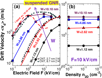
The computed average drift velocity limited by intrinsic phonons is plotted in Fig. 1a as a function of for suspended sub-10 nm GNRs and for a carrier density 1012 cm-2. strongly varies within the considered interval and a maximum appears at high electric field (). For , can be fitted by means of the Caughey-Thomas model, i.e. , where , is the intrinsic LF mobility and is the peak velocity, which ranges from to m/s, depending on (Table 1). does not saturate with , analogously to what has been observed in the case of zigzag CNTs Pennington and Goldsman (2003); Perebeinos et al. (2005). As shown in Fig. 1a, slightly decreases for increasing Pennington and Goldsman (2003). However, in constrast to Pennington and Goldsman (2003), the negative differential mobility (NDM) cannot be explained by the increased number of populated states in the second subband with smaller . Indeed, as in Perebeinos et al. (2005), we have verified for 10 nm that such effect is much more pronounced if we fictitiously limit transport to only one subband (red dashed line in Fig. 1a).
| 1.12 | 310 | 1.7 | 4.86 | 12000 | 1.4 | ||
| 2.62 | 2700 | 1.3 | 10.10 | 80000 | 2 |
The velocity peak can be explained by the combined effect of the quasi-linear dispersion relation in GNRs and the strong increase of optical EM at high , which increases the occurrence of backscattering events therefore reducing the average velocity. If we follow the story of a single electron, we can see that as increases, instantaneous electron velocity cannot increase beyond the limit imposed by the dispersion relation: any backscattering event will invert the instantaneous velocity sign and therefore reduce the average velocity. Therefore, in the absence of optical phonon EM, the drift velocity would saturate to about m/s. The onset of optical phonon EM makes peak at a fraction of that value and then decrease with . We believe that the very same mechanism explains also the NDM in zigzag CNTs, as well as in graphene Li et al. (2007), even if it has not been proposed before Pennington and Goldsman (2003); Perebeinos et al. (2005). One can also see that the peak velocity increases with . Indeed, if is the optical phonon energy ( meV for LA mode), the current can be estimated as Freitag et al. (2009), where is the Fermi velocity. Since and the Fermi wavevector , we obtain .
The threshold field strongly decreases with , because of the increased mean free path , which allows electrons to gain energy required to emit optical phonons at lower . can be roughly extimated by imposing the cutoff energy for optical EM equal to the mean kinetic energy gained between two scattering events, i.e. . Since by increasing from 1 to 10 nm, increases from nm to 1 m Betti et al. (2011a), decreases from kV/cm to kV/cm. We remark also that the obtained values for are in agreement with those found for zigzag CNTs with a circumference comparable with the considered , both in linear and in non-linear regimes Pennington and Goldsman (2003). In Fig. 1b, is plotted as a function of for 10 kV/cm: does not depend on even in the degenerate regime ( 1012 cm-2), where PEP limits up to the 50% of the scattering events.
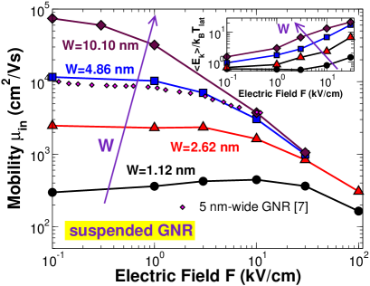
In Fig. 2, we show the intrinsic mobility as a function of for 1012 cm-2. Since in the linear transport regime , is constant for and decreases above as with . In addition, the narrower the ribbons, the stronger the suppression due to lateral confinement. Results are in good agreement with a multi-subband model for nm Zeng et al. (2009). In the inset of Fig. 2, the average kinetic electron energy in units of is shown as a function of for 1012 cm-2. While for low 0.1 kV/cm electrons tend to remain near the first conduction subband edge and for the narrowest ribbons, for high field kV/m, and higher energy states are occupied. Note also that increases with , since subbands become closer, allowing electrons to populate higher subbands.
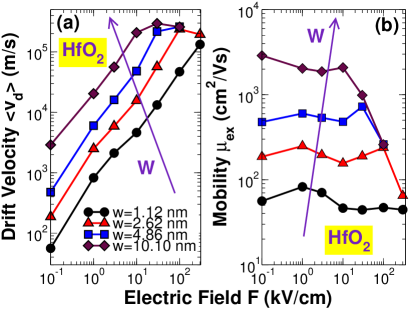
In Fig. 3a and 3b the average drift velocity and the mobility are shown, respectively, as a function of for GNRs deposited on HfO2 Betti et al. (2011a) including the effect of SO phonons ( 1012 cm-2), through the first SO(1) and second SO(2) modes ( 12.4 meV for SO(1) mode). With respect to the suspended GNR case, , as well as mobility in GNR on HfO2 are almost one order of magnitude smaller in the LF regime, while similar values are obtained for high field, as already noted for graphene on HfO2 Li et al. (2007). As in graphene Li et al. (2007), deposition on HfO2 leads to an extension of the linear region to fields up to a factor 10 larger than those corresponding to suspended GNRs. For narrow ribbons, does not saturate even for kV/cm.
In order to understand the different behaviour in suspended and deposited GNR on HfO2, in Fig. 4a we show the distribution function as a function of , where is the first subband edge, for 1 and 10 kV/cm ( nm) for GNRs, both suspended and deposited on HfO2. At low fields, decreases rapidly with energy in both cases, showing, unlike graphene, sharp peaks due to intersubband scattering. At high fields instead, electrons are excited up to energies close or above 1 eV, increasing (inset of Fig. 2).
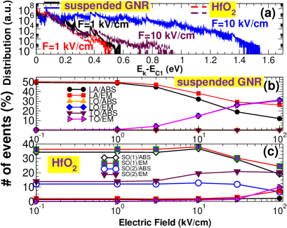
As expected, deposition on HfO2 leads to a shorter high energy tail compared to that in intrinsic GNR (Fig. 4a) due to the introduction of an additional channel for energy and momentum relaxation which increases total scattering rate and pushes electrons down to lower average electron energy. As for graphene on HfO2 Li et al. (2007), the rough absence of degradation of at high can be explained by the reduced population in the high energy tail, i.e. by a smaller amount of electrons in the nonlinear dispersion energy region where the band velocity is smaller, which more than counterbalances the decrease of resulting from the increased total scattering rate when depositing GNR on substrate. In order to explain the increase of the interval where shows a linear behavior in the GNR on HfO2 case, in Fig. 4b and 4c we show the relative ratio of scattering events for the different mechanisms as a function of for 5 nm-wide suspended GNR and GNR on HfO2, respectively. For intrinsic GNR and kV/cm, the main scattering events involve absorption (ABS) and EM of LA phonons (Fig. 4b). For kV/cm, optical phonon EM (of both LO and TO phonons) becomes predominant, increasing up to 30% of the total number of events. For GNR on HfO2 instead, scattering involving SO(1) phonons happens very often already for kV/cm whereas rates of LA, LO and TO phonons are limited to few percents even for high fields, as can be seen in Fig. 4c. In particular, the observed large absorption rate of SO(1) phonons (Fig. 4c), which is associated to the high Bose-Einstein occupation factor, appears to counterbalance SO(1) emission even at high , and is the responsible of the extension of the linear region up to fields of 10 kV/cm or above, depending on .
In conclusion, we have performed a FB investigation of the dependence of drift velocity and mobility on the electric fields in GNRs. Suspended GNRs exhibit a drift velocity peak and then a NDM for large electric field, as also observed in zigzag CNTs. This property is due to the combined effect of quasi-linear dispersion relation and the emission of optical phonons. In particular, the maxima occur for a threshold field . Depositing GNR on HfO2 substrate strongly degrades at low field by a factor , whereas at high fields no degradation is observed Li et al. (2007). Furthermore, in deposited GNRs velocity saturation and peak are shifted at higher , due to the compensation of SO absorption and EM mechanisms.
Authors gratefully acknowledge support from the EU FP7 Project NANOSIL (n. 216171), GRAND (n. 215752) grants, and by the MIUR-PRIN project GRANFET (Prot. 2008S2CLJ9) via the IUNET consortium.
References
- Wang et al. (2008) X. Wang, Y. Ouyang, X. Li, H. Wang, J. Guo, and H. Dai, Phys. Rev. Lett. 100, 206803 (2008).
- Betti et al. (2011) A. Betti, G. Fiori, and G. Iannaccone, IEEE Trans. Electron Devices 58, 2824 (2011).
- Yang and Murali (2010) Y. Yang and R. Murali, IEEE Elec. Dev. Lett. 31, 237 (2010).
- Betti et al. (2011a) A. Betti, G. Fiori, and G. Iannaccone, Appl. Phys. Lett. 98, 212111 (2011a).
- Briggs and Leburton (1988) S. Briggs and J. P. Leburton, Phys. Rev. B 38, 8163 (1988).
- Mickevicius et al. (1992) R. Mickevicius, V. V. Mitin, K. W. Kim, and M. A. Stroscio, Semicond. Sci. Technol. 7, B299 (1992).
- Zeng et al. (2009) L. Zeng, X. Y. Liu, G. Du, J. F. Kang, and R. Q. Han, Int. Conf. Simulation of Semiconductor Processes and Devices pp. 1–4 (2009).
- Huang et al. (2011) D. Huang, G. Gumbs, and O. Roslyak, Phys. Rev. B 83, 115405 (2011).
- Bresciani et al. (2010) M. Bresciani, P. Palestri, and D. Esseni, Solid-State Electronics 54, 1015 (2010).
- Lugli and Ferry (1985) P. Lugli and D. K. Ferry, IEEE Trans. Electron Devices 32, 2431 (1985).
- Saito et al. (2003) R. Saito, G. Dresselhaus, and M. Dresselhaus, Imperial College Press, London (2003).
- Jacoboni and Reggiani (1983) C. Jacoboni and L. Reggiani, Rev. Mod. Phys. 55, 645 (1983).
- (13) See EPAPS supplementary material at [].
- Pennington and Goldsman (2003) G. Pennington and N. Goldsman, Phys. Rev. B 68, 045426 (2003).
- Perebeinos et al. (2005) V. Perebeinos, J. Tersoff, and P. Avouris, Phys. Rev. Lett. 94, 086802 (2005).
- Li et al. (2007) X. Li, E. A. Barry, J. M. Zavada, M. Buongiorno Nardelli, and K. W. Kim, Appl. Phys. Lett. 97, 232105 (2010).
- Freitag et al. (2009) M. Freitag, M. Steiner, Y. Martin, V. Perebeinos, Z. Chen, J. C. Tsang, and P. Avouris, Nano Lett. 9, 1883 (2009).