Magnetotransport Properties of Quasi-Free Standing Epitaxial Graphene Bilayer on SiC: Evidence for Bernal Stacking
Abstract
We investigate the magnetotransport properties of quasi-free standing epitaxial graphene bilayer on SiC, grown by atmospheric pressure graphitization in Ar, followed by H2 intercalation. At the charge neutrality point the longitudinal resistance shows an insulating behavior, which follows a temperature dependence consistent with variable range hopping transport in a gapped state. In a perpendicular magnetic field, we observe quantum Hall states (QHSs) both at filling factors () multiple of four (), as well as broken valley symmetry QHSs at and . These results unambiguously show that the quasi-free standing graphene bilayer grown on the Si-face of SiC exhibits Bernal stacking.
Keywords: graphene, bilayer, SiC, quantum Hall, Bernal stacking
Graphene bilayers in Bernal stacking novoselov_natphys06 exhibit a transverse electric field tunable band-gap mccannprl06 ; min , as evidenced by angle-resolved photoemission ohta and transport measurements castro07 ; oostinga , a property that renders this material attractive for device applications. Bernal stacking is the lowest energy structure, and is found in the natural graphite crystal. Recent studies of graphene bilayer grown on SiC riedl and Cu lee ; yan have suggested the presence of Bernal stacking, based primarily on electron microscopy and Raman spectroscopy. However, there has been no firm evidence of Bernal stacking based on electron transport, which in turn would allow an assessment of its potential role for electronic devices xia . It is therefore of high interest to explore the electron transport in grown graphene bilayers, in order to determine the stacking of the layers and the key transport properties.
Here we investigate the transport properties of epitaxial graphene bilayer grown by atmospheric pressure graphitization of SiC followed by H2 intercalation, which renders the graphene quasi-free standing. Using top gated Hall bars with Al2O3 dielectric we probe the magneto-transport up to magnetic fields of 30 T and temperatures down to 0.3 K. The devices show a high field-effect mobility of 2,600 - 4,400 cm2/Vs, which changes little from room temperature down to 0.3 K, as well as a strong insulating behavior near the charge neutrality point. The magneto-transport data reveal quantum Hall states (QHSs) at filling factors , consistent with the four-fold, spin and valley degenerate Landau levels (LL) in Bernal stacked (A-B) graphene bilayer. More interestingly, the data also reveal developing broken valley symmetry QHSs at filling factors and , which testify to the high sample quality. Further supported by Raman spectroscopy and low energy electron microscopy (LEEM) data, these results unambiguously show that the quasi-free-standing epitaxial graphene bilayer grown on the Si face of SiC substrates exhibits Bernal stacking.
The graphene bilayer films studied in this paper are produced via a two step process beginning with a starting substrate of 6H-SiC(0001) (Si-face, 2.11011 cm, II-VI Incorporated). Prior to graphitization, the substrate is hydrogen etched (45 H2 - Ar mixture) at 1350 ∘C to produce well-ordered atomic terraces of SiC. Subsequently, the SiC sample is heated to 1000 ∘C in a 10 H2 - Ar mixture, and then further heated to 1550 ∘C in an Ar atmosphere emtsev ; pan . This graphitization process results in the growth of an electrically active graphene layer on top of the buffer layer, covalently bound to the substrate. Finally, hydrogen intercalation was carried out using 45 H2 - Ar mixture at 800 ∘C riedl , in order to decouple the buffer layer from the substrate. As we show here, the two graphene layers, a formally buffer layer (decoupled via hydrogen intercalation) and a monolayer graphene (formed via graphitization process), are in Bernal stacking.
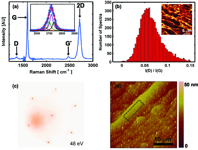
Both the number of layers and the quality of the resulting material are probed by Raman spectroscopy acquired over a 2525 m region, using a 532 nm excitation wavelength, 5 mW power, and 500 nm spot size. Figure 1(a) shows a typical Raman spectrum of the graphene bilayer sample in which the contribution from SiC substrate has been subtracted. Well defined spectral features characteristic of graphene’s G (1600 cm-1) and 2D-band (2700 cm-1) are observed. The 2D-band was well fit utilizing four Lorentzian peaks each with a width of 35 cm-1 confirming that the presence of graphene bilayer [Fig. 1(a) inset]. The Raman spectra indicate that the sample is of high quality as the intensity ratio of the defect induced D-band to G-band, while present is less than 0.1 for the great majority of the sample area [Fig. 1(b)]. The presence of graphene bilayer is further confirmed by the energy dependence spectrum of the specular electron reflection ohta2008 , and by the well ordered 6-fold low energy electron diffraction (LEED) pattern acquired with LEEM [Fig. 1(c)]. No turbostatic disorder was observed.
To probe the transport properties of these graphene bilayers we fabricate top-gated Hall bars. The Hall bar location on the substrate is first chosen using optical and atomic force microscopy (AFM) in order to identify an appropriately wide terrace [Fig. 1(d)]. The dashed contour of Fig. 1(d) is an example of an 8 m-wide terrace, onto which a Hall bar is subsequently defined. Raman imaging confirms that there is only graphene bilayer within these terraces, as panel (b) inset shows that the 2D mode is rather uniform inside terraces. E-beam lithography and O2 plasma etching are used to pattern the Hall bar active area; the graphene is etched outside the Hall bar to prevent parallel current flow. Metal contacts are realized using a second e-beam lithography step, followed by a 40 nm Ni deposition and lift-off. To deposit the Al2O3 gate dielectric, we first deposit a 1.5 nm thick Al film. The sample is then exposed to ambient, and transferred to an atomic layer deposition (ALD) chamber. The ambient exposure causes the Al interfacial layer to fully oxidize dignam , and provides nucleation centers for the subsequent ALD process. A 15 nm thick Al2O3 top dielectric film is then deposited using trimethylaluminum as Al source, and H2O as an oxidizer kim . A third e-beam lithography step, followed by Ni deposition and lift-off are used to pattern the top gate [Fig. 2(a) inset]. The corresponding dielectric capacitance for this stack is 245 nF/cm2, with an average dielectric constant of .
Four point longitudinal () and Hall () resistivity measurements are performed at temperatures () down to 0.3 K, and magnetic fields () up to 30 T, using low-current, low-frequency lock-in techniques. The carrier density (), and its dependence on the top gate voltage () are determined from Hall measurements, as well as the filling factors of the quantum Hall states observed in high magnetic fields. The longitudinal () and Hall () conductivities are determined via a tensor inversion from the measured resistivities.
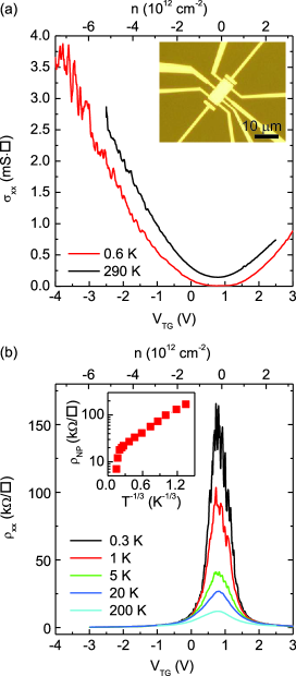
In Fig. 2(a) we show vs. , measured at K and 0.6 K, and at = 0 T, revealing an ambipolar characteristic with a charge neutrality point at a positive value. Away from the charge neutrality point, the vs. data show a linear dependence up to the highest values, with a corresponding field-effect mobility of 2,600 - 4,400 cm2/Vs at =290 K mobility . At K, where the measurement was performed in a wider range, the vs. linear dependence persists down to -4 V, for a gate voltage overdrive of up to 5 V. The linear vs. dependence contrasts data reported in mono-layer graphene, where neutral impurity scattering, which is density independent, limits the conductivity at high values. In contrast, the neutral impurity scattering remains proportional to in graphene bilayers adam08 .
Figure 2(b) shows vs. at different values, measured at T. Remarkably, measured near the charge neutrality point is strongly temperature dependent, with an insulating behavior. The insulating phase at the charge neutrality point suggests an energy gap, and contrasts data from mono-layer graphene with comparable mobility, where at the charge neutrality point is weakly temperature dependent. In contrast, graphene bilayers in the presence of an applied transverse electric field open a tunable energy gap between the conduction and valence bands, thanks to the layer on-site energy asymmetry mccannprl06 . We posit the presence of a transverse electric field in our samples, due to unintentional doping and the asymmetry of the device structure. The inset of Fig. 2(b) shows the -dependence of the resistivity measured at the charge neutrality point (). The data clearly follow a dependence for lower than K, indicating that variable range hopping rather than thermally activated conduction controls the electron transport at low temperatures. This has been attributed to disorder-induced localized states in the gap, which reduce the effective energy gap zou ; taychatanapat , and render the -dependence of the weaker than the exponential dependence expected for a band insulator with an energy gap ; is the Boltzmann constant. The extracted value corresponding to Fig. 2(b) inset data is 0.6 K, similar to previously reported values on exfoliated graphene bilayers zou ; oostinga . A fit of the vs. data of Fig. 2(b) inset to the exponential dependence for K, yields an energy gap at the charge neutrality point of meV.
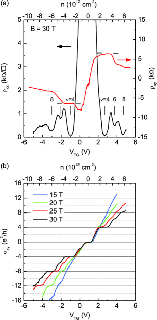
While Fig. 2 data at the charge neutrality point show an energy gap, suggestive of a graphene bilayer, the most important finding of this study is presented in Fig. 3. Figure 3(a) shows and vs. , measured at a high magnetic field of T, and a temperature K. The data reveal strong QHSs at integer filling factors , and , marked by vanishing or local minima in , and corresponding plateaus. The QHSs at integer filling factors multiple of four in Fig. 3 stem from the four-fold degeneracy associated with spin and valley of each Landau level, and unambiguously identify the material as being a Bernal stacked (A-B) graphene bilayer. In contrast, thanks to the -Berry phase of chiral Dirac fermions, the strongest QHSs in mono-layer graphene are present at integer fillings , 6, 10, etc… novoselov05 ; zhang05 Figure 3(b) data show vs. at different values of the -field. The plateaus at values, which become stronger with increasing the -field confirm the presence of QHSs at fillings , 8, 12 consistent with a Bernal stacked graphene bilayer. More interestingly, Fig. 3 data reveal a strong QHS at , and a developing QHS at . While a possible explanation for the QHS is a mixture of graphene mono- and bilayer, this is ruled out by the absence of the other QHSs associated with mono-layer graphene, in particular the QHS. The absence of graphene monolayers is further corroborated by LEEM measurements. On the other hand, the presence of and QHSs is fully consistent with a graphene bilayer in the presence of a transverse electric field, a finding which is also consistent with Fig. 2 data. We expand below on this argument.
At zero transverse electric field (), an eight-fold degenerate Landau level (LL) is located at zero energy (charge neutrality point); it consists of the = 0, 1 LLs with their respective valley and spin degeneracies. The , 1 LLs are layer polarized and split in the presence of a transverse -field depending on the on-site energy of the layer (valley) degree of freedom mccannprl06 , leading to a QHS at . Similarly, the presence of a transverse -field breaks the valley degeneracy of LLs nakamura , but the corresponding energy splitting is smaller than that of , 1 LLs. This explains the absence of QHS in exfoliated graphene bilayers on SiO2, where the LL disorder broadening can obscure the -field induced splitting. In that regard, the observation of a QHS in quasi-free standing graphene bilayers is interesting, and testifies to a reduced disorder and LL broadening in these samples, by comparison to dual-gated graphene bilayers on SiO2 substrates, and with a similar top-gate stack kim11 . We note that back-gated graphene bilayers on SiO2 samples can exhibit higher mobilities zhao .
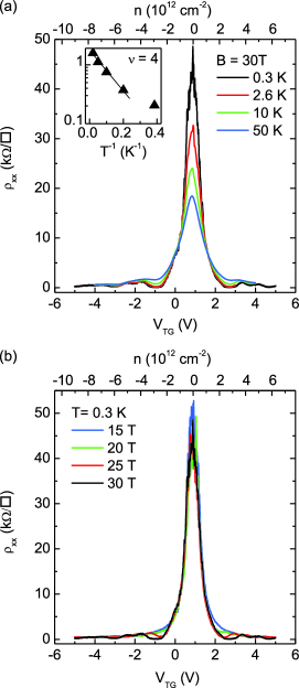
In the remainder, we explore further the QHS in these samples. Depending on the transverse -field, the QHS in graphene bilayers can be either spin-polarized at small -fields, or valley- (layer) polarized at large -fields gorbar10 ; toke10 . If the -field is varied at a given perpendicular magnetic field, the QHS undergoes a transition from spin-to-valley-polarized at a critical -field (). Experimental studies weitz ; kim11 on dual-gated A-B (Bernal) graphene bilayers exfoliated from natural graphite show a linear dependence of on , with a slope of 12-18 (mV/nm)T-1. Figure 4(a) shows vs. , measured at = 30 T, and at different temperatures. The data reveal an insulating phase near the charge neutrality point, consistent with a LL splitting at zero energy responsible for the presence of the QHS of Fig. 3(b). The inset of Fig. 4(a) shows the Arrhenius plot of vs. at QHS; the data follow an activated -dependence, with an energy gap K for . Figure 4(b) shows vs. measured at K and at different values of the -field. Figure 4(b) data show a weak dependence of on at . This finding, analyzed by comparison with existing data in exfoliated A-B bilayers kim11 suggest that the is neither spin-polarized or valley-polarized in the range of -fields probed here, but rather in the vicinity of the spin-to-valley-polarized transition (see supplementary material). Indeed, if the QHS was spin polarized, we would expect at to increase with . Conversely, if the QHS was valley polarized a decrease of with the -field is expected. This argument provides us with an estimate of the transverse -field across the bilayer of 0.350.07 V/nm.
In summary, we investigate the magnetotransport in quasi-free-standing graphene bilayers on SiC. We observe QHSs at fillings , consistent with a Bernal stacked graphene bilayer in the presence of a transverse field. An insulating state observed at T, near the charge neutrality point indicates the opening of an energy gap, in agreement with the expected response of a Bernal stacked graphene bilayer. These findings corroborated with earlier microscopy studies riedl unambiguously identify the Bernal stacking arrangement of graphene bilayers on the Si-face of SiC substrates, and render this system particularly attractive for electronic and optoelectronic device applications, thanks to its high mobility, tunable energy gap, and high on/off ratio.
The work at University of Texas at Austin was supported by NRI, DARPA, NSF (DMR-0819860), and the NINE program. Part of this work was performed at the National High Magnetic Field Laboratory, which is supported by NSF (DMR-0654118), the State of Florida, and the DOE. The work at Sandia Labs was supported by LDRD, and performed in part at CINT, a US DOE, Office of Basic Energy Sciences user facility (DE-AC04-94AL85000). Sandia is a multiprogram laboratory operated by Sandia Corporation, a Lockheed Martin company, for the US DOE’s National Nuclear Security Administration under contract DE-AC04-94AL85000. We are grateful to Guild Copeland and Anthony McDonald for sample preparation and characterization, partly supported by the US DOE Office of Basic Energy Sciences, Division of Materials Science and Engineering.
References
- (1) K. S. Novoselov et al., Nature Phys. 2, 177 (2006).
- (2) E. McCann and V. I. Fal’ko, Phys. Rev. Lett. 96, 086805 (2006).
- (3) H. Min, B. Sahu, S. K. Banerjee, A. H. MacDonald, Phys. Rev. B75, 155115 (2007).
- (4) T. Ohta et al., Science 313, 951 (2006).
- (5) E. V. Castro et al., Phys. Rev. Lett. 99, 216802 (2007).
- (6) J. B. Oostinga et al., Nature Mat. 7, 151 (2008).
- (7) C. Riedl, C. Coletti, T. Iwasaki, A. A. Zakharov, U. Starke, Phys. Rev. Lett. 103, 246804 (2009).
- (8) S. Lee, K. Lee, Z. Zhong, Nano Lett. 10, 4702 (2010).
- (9) K. Yan, H. Peng, Y. Zhou, H. Li, Z. Liu, Nano Lett. 11, 1106 (2011).
- (10) F. Xia, D. Farmer, Y.-M. Lin, P. Avouris, Nano Lett. 10, 715 (2010).
- (11) K. V. Emtsev et al., Nature Materials 8, 203 (2009).
- (12) W. Pan et al., Appl. Phys. Lett. 97, 252101 (2010).
- (13) T. Ohta et al., New J. Phys. 10, 023034 (2008).
- (14) M. J. Dignam, W. R. Fawcett, H. Bohni, J. Electrochem Soc. 113, 656 (1966).
- (15) S. Kim et al., Appl. Phys. Lett. 94, 062107 (2009).
- (16) The measured field-effect mobility varies depending on the pair of contacts used to probe the longitudinal resistance.
- (17) S. Adam, S. Das Sarma, Phys. Rev. B77, 115436 (2008)
- (18) E. McCann, Phys. Rev. B74, 161403(R) (2006).
- (19) K. Zou and J. Zhu, Phys. Rev. B82, 081407(R) (2010).
- (20) T. Taychatanapat and P. Jarrilo-Herrero, Phys. Rev. Lett. 105, 166601 (2010).
- (21) K. S. Novoselov, A. K. Geim, S. V. Morozov, D. Jiang, M. I. Katsnelson, I. V. Grigorieva, S. V. Dubonos, A. A. Firsov, Nature 438, 197 (2005).
- (22) Y. B. Zhang, Y. W. Tan, H. L. Stormer, P. Kim, Nature 438, 201 (2005).
- (23) M. Nakamura, E. V. Castro, B. Dora, Phys. Rev. Lett. 103, 266804 (2009).
- (24) S. Kim, K. Lee, E. Tutuc, Phys. Rev. Lett. 107, 016803 (2011).
- (25) Y. Zhao, P. Cadden-Zimansky, Z. Jiang, P. Kim, Phys. Rev. Lett. 104, 066801 (2010).
- (26) E. V. Gorbar, V. P. Gusynin, and V. A. Miransky, Phys. Rev. B81, 155451 (2010).
- (27) C. Tőke and V. I. Fal’ko, Phys. Rev. B83, 159901 (2011).
- (28) R. T. Wietz, M. T. Allen, B. E. Feldman, J. Martin, A. Yacoby, Science 330, 812 (2010).