Silicon Photomultipliers for High Energy Physics Detectors
Abstract
In this paper I want to review the current status of development of multi-pixel silicon-based avalanche photo-diodes operated in Geiger mode, also known as Silicon Photomultipliers (SiPM). Particular emphasis is given to the application of this type of photo-sensors in high energy physics detectors.
keywords:
silicon photo-multiplier, light detection, photon counting.1 Introduction
Multi-pixel silicon-based avalanche photo-diodes operated in Geiger mode (SiPM) have become increasingly popular in HEP, as well as medical and astroparticle physics applications. What makes them attractive alternatives to the more conventional photomultiplier tubes (PMT) is for instance the insensitivity to magnetic fields and in some cases the higher photon detection efficiency, the compactness and robustness, and the low cost. With respect to avalanche photo-diodes (APD) SiPMs offer a high intrinsic gain (105-107) which significantly simplifies the readout electronics, and increases the response stability to voltage or temperature changes. SiPMs are also insensitive to ionizing radiation, i.e. the nuclear counter effect.
Additionally, SiPMs provide fast timing (100 ps FWHM for a single photon) and single photon counting capabilities.
In this paper I review the products available on the market in terms of their basic properties and I discuss how each property influences or limits the design of typical HEP detectors.
The zoo of names referring to multi-pixel Geiger-mode avalanche photo-diodes (SiPM, G-APD, SSPM, MRS APD, AMPD, MPPC, etc.) is only partially representative of the increasing variety in performance between the various products. We shall see what the key parameters are to characterize a SiPM111I will adopt in this paper the name SiPM to generically refer to them all. and how the various products are comparing on the basis of these parameters.
Good SiPMs by themselves do not make up for a whole HEP detector. Therefore, it is important to review the current status of SiPM specific readout chips as well as the implications of SiPMs on the design of a multi-channel detector. Issues like the need of individual SiPM bias adjustment and of the calibration and monitoring system are addressed.
2 SiPM basic properties
The equivalent electric circuit of a SiPM is the parallel sum of as many diodes as the SiPM has individual pixels, typically 100-2000 mm-2. To all diodes a common inverse bias voltage is provided to operate the device a few volts above the breakdown point, . Each diode requires an active quenching of the Geiger discharge, normally obtained by connecting a resistor in series with the diode.
2.1 Signal time characteristics
The time needed for a pixel to become active again after a discharge is known as the pixel recovery time, . This is the product of the pixel quenching resistor, Rq, and the pixel capacitance, Cpix. The value of Rq has to be larger than 100 k to be able to quench the avalanche and can be as large as 20 M in some cases [1]. The value of Cpix scales with the pixel area and can be 20-150 fF. Thereby, can range between a few 10 ns to a few s. It has to be kept in mind that polysilicon resistors are temperature dependent, and so is the pixel recovery time. Alternative quenching methods are being tested as well like integrated FET circuits in the silicon wafer [2] or CMOS quenching circuits in the case of digital SiPMs [3].
2.2 Gain
The SiPM gain, M is defined as the number of electric charges generated by one Geiger discharge in a SiPM pixel. This value is quite stable for Geiger discharges, and can be around 105-107. This is why a SiPM single pixel signal can be seen directly on the oscilloscope without preamplification as a signal of a few mV on a load of 50 . The pixel recovery time affects the design of the readout electronics as the integration or shaping time needed to exploit the large SiPM gain depends on the length of the signal. The effective SiPM gain, M is the number of electric charges measured in a given time interval after the Geiger discharge of one pixel, M M. When reading the SiPM signal through a small decoupling capacitor or with a short shaping time, it is sometimes necessary to use a preamplification factor of 10-50. More discussion on the interplay between SiPM signal and design of the readout electronics is provided in section 5.
2.3 Dark rate and after-pulse
In the absence of light a signal in the SiPM can be produced by carriers thermally generated in the depletion region.
Secondary avalanches, the so called after-pulses, can follow a primary one caused by the release of carriers trapped in the silicon crystal during the primary Geiger avalanche.
The first contribution is temperature dependent and approximately doubles for an increase of eight degrees. The second one depends on the pixel recovery time, the shorter is (20% for Hamamatsu MPPCs [5] with 30 ns, 3% for CPTA/Photonique [6] with 150 ns, [7]) the larger is the contribution from after-pulse. It also increases exponentially with the over-voltage222It has become SiPM jargon to refer to the operation voltage point above breakdown as over-voltage.
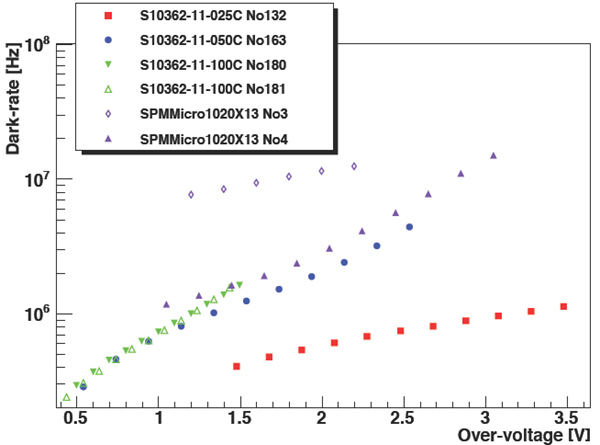
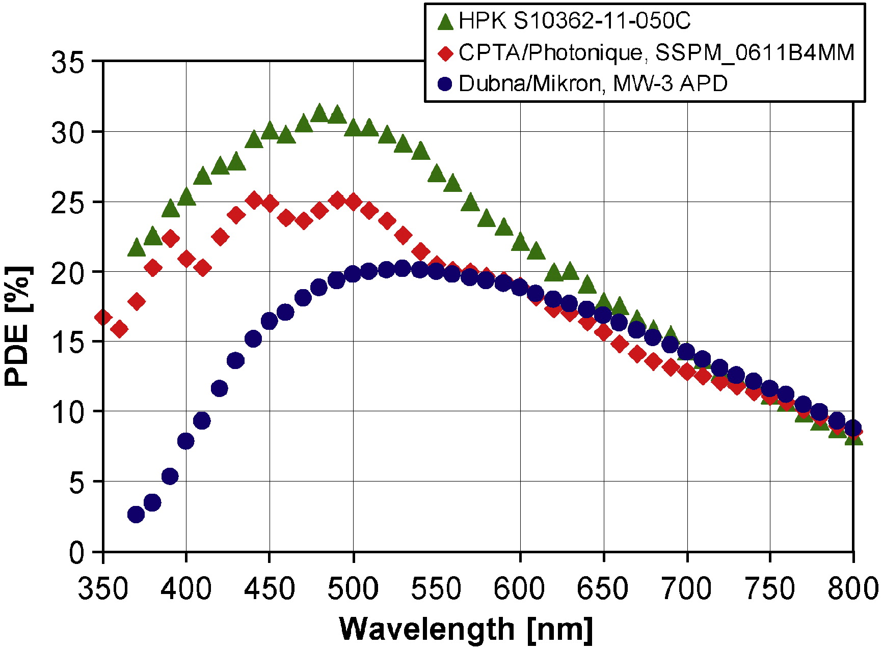
The dark rate of SiPMs can largely vary between 105-107 Hz. As shown (figure 1) in a characterization study reported in [4], the dark rate depends exponentially on the voltage above breakdown at which the device is operated (higher dark rate for higher over-voltage, or . For simplicity I will use this abbreviation in this paper.) and on the pixel capacitance (higher dark rate for larger capacitance at the same over-voltage). In addition, the dark rate is strongly influenced by the quality of the silicon wafer used for the SiPM production and by the level of cleanliness during the implant processes.
2.4 Optical crosstalk
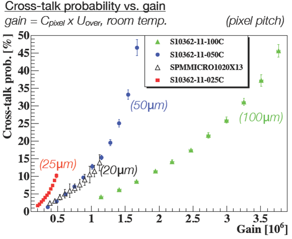
During the avalanche process in a p-n junction photons in the visible range are emitted. A typical number if of about 310-5 photons per charge carrier with a wavelength less than 1 m [8]. If these photons reach a neighboring pixel an additional avalanche can be caused. This effect is known as optical crosstalk between pixels and can occur as often as 30-40% of the times a Geiger discharge takes place. The optical crosstalk increases exponentially with the SiPM gain. This is the combined effect of two factors: The number of photons generated in the discharge increases with the number of carriers, and the avalange trigger efficiency increases with increasing over-voltage.
Photons traveling directly between pixels can be stopped by optical tranches in the silicon.
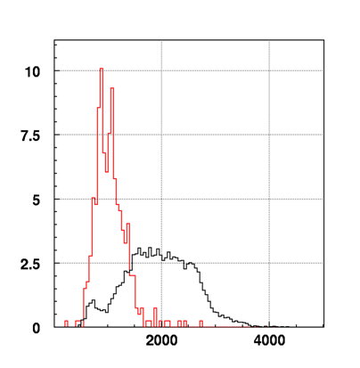
This technique introduced first by CPTA/Photonique [9], and later on used by SensL [10] and STMicroelectronics [11], reduces significantly the optical crosstalk to 1-3%. The remaining effect is due to absorbed photons in the silicon bulk, much below the optical tranch, which are later re-emitted at an angle that allows them to reach a neighboring pixel. This last effect can hardly be avoided. A comparison study from [4] of crosstalk of various devices is reported in figure 2.
3 SiPM response
The SiPM response is the sum of the charges from all the pixels fired by a given amount of photons impinging on the SiPM active area. For very low number of impinging photons, N, the number of pixels fired, is given by the product of N and the photon detection efficiency (PDE). is strongly non-linear, and ignoring recovery time effects it saturates to the total number of pixels in a device for very large number of impinging photons.
3.1 Photon detection efficiency
The photon detection efficiency can be factorized in three components:
| (1) |
where is the wavelength-dependent quantum efficiency of a pixel, is the geometric fill factor of the SiPM, and is the wavelength-, voltage- and temperature-dependent probability for a photoelectron to trigger a breakdown, or Geiger discharge.
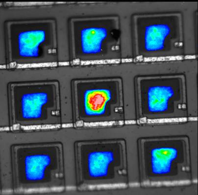
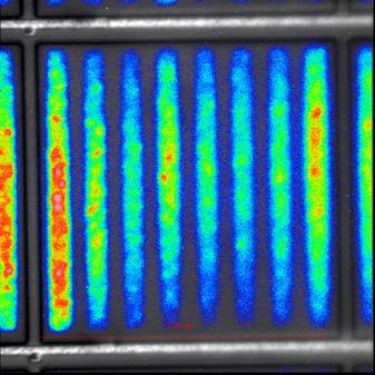
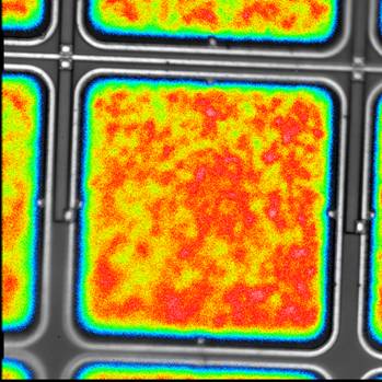
The fill factor depends inversely on the number of pixels per unit area, and on the quenching technology used. Also the process used to dope the silicon can have an effect on the fill factor. Examples of photo-emission spectra for SiPM from different producers are given in figure 3. The colored area in the pictures correspond to the active areas in the pixel and the color scale gives an impression of the electric field uniformity across the pixel. While the oldest devices have = 20-30%, with recent developments these values have increased to 70% for CPTA/Photonique and 50% for FBK-irst [13] SiPMs.
Concerning the wavelength sensitivity, the standard SiPM structure from most of the producers (CPTA/Photonique, SensL, FBK-irst, MEPhI/PULSAR [1]) is an n-doped implant on a p-type substrate. In this structure the thickness of the depleted region ranges from 3 to 10 m and the depth of the n+-p junction ranges from 0.3 to 1 m [14]. This structure is optimal for green-red light detection (1-3 m absorption depth in silicon). To enhance the sensitivity to blue/UV light (400-450 nm) some producers (Hamamatsu, and recently MEPhI/PULSAR and STMicroelectronics) have opted for an inverted structure with a p-doped implant on an n-type substrate. In this case the blue/UV photons (absorption depth in silicon 100-500 nm) convert in the p+ region close to the surface. In the p+ region the produced electrons drift towards the multiplication region, or p+-n junction, while the holes drift towards the surface of the photodetector, or cathode. Electrons have a larger probability to trigger a breakdown in silicon than holes due to their larger ionization coefficient. A conversion in the p+ layer has the highest probability to start a breakdown [15].
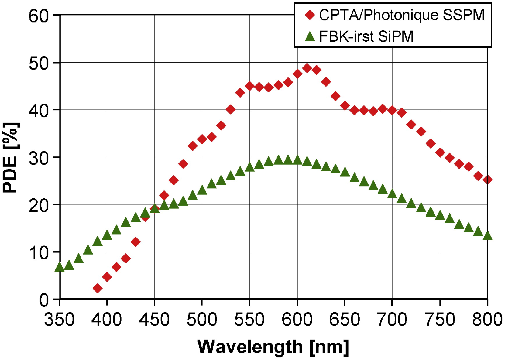
Recent comparison studies of PDE from various SiPMs have been performed for example in [4, 7]. Figure 4 reports results from [7]. These measurements are properly subtracting the influence of optical-crosstalk and after-pulse, which if not accounted for leads to an enhanced PDE. Currently the best PDE in the blue/UV range is provided by the Hamamatsu MPPC (PDE 35% for devices with 100 m pixel size, and PDE 30% for devices with pixels of 50 m size). A PDE 40-45% has been obtained by the n-on-p devices from CPTA/Photonique.
3.2 Response function and dynamic range
Due to the limited number of pixels and the finite pixel recovery time, the SiPM is an intrinsically non-linear device. The response function of a SiPM correlates the observed number of pixels fired, , to the effective number of photo-electrons generated, , including crosstalk and after-pulses. The response of a SiPM can be approximated by the function
| (2) |
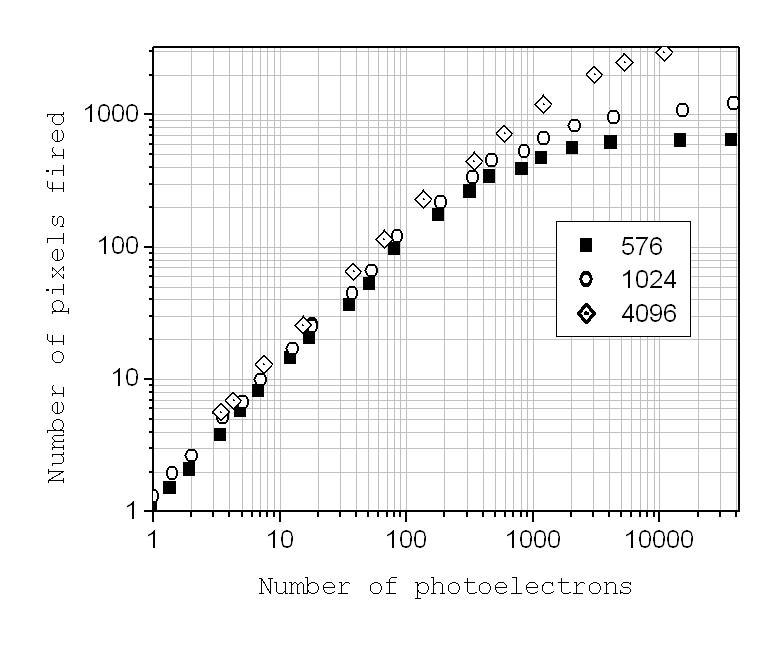
with being the maximum number of fired pixels in a SiPM. This formula is a useful approximation for the case of uniform light distribution over the pixels and short light pulses compared to the pixel recovery time. Signals equivalent to 80% of the total number of pixels in a SiPM are underestimated by 50% with respect to the measurement of a linear device. This effect limits the dynamic range of a system and reduces the acceptable spread in light yield of the system components. In addition, it requires a correction of the non-linear response which can be either an individual or a global curve, depending on how large the spread in PDE and crosstalk is of the various SiPMs in the system. Measurements of the SiPM response curve for MEPhI/PULSAR devices with various number of pixels are presented in figure 5.
A significant improvement of the SiPM dynamic range is provided by the innovative design of the MAPD from Zecotek [17]. This is a non-conventional SiPM in the sense that it consists of a double n-p-n-p junction with micro-well structures located at a depth of 2-3 m below the surface. The multiplication regions are just in front of the wells. This technique allows the quenching of the discharge in the absence of an additional resistor. In this way a pixel density of 10000-40000 mm-2 is possible on an area up to 33 mm2.
4 SiPM application to HEP detectors
One of the main advantages of SiPMs in the application for HEP detectors is the possibility to significantly increase the detector granularity with respect to PMT- and even APD-based readout designs. Plastic scintillator with wavelength shifter (WLS) readout is a very attractive solution for detectors which require high granularity. Extreme examples are calorimeters for particle flow applications, as those designed for the future linear collider detectors [18]. Such calorimeters require single cells with a size of 3.03.0 cm2 and even 1.04.5 cm2. Furthermore, the calorimeters are inside the spectrometer magnet so that the photodetectors used in the readout must be magnetic field insensitive. About five to ten million single cells are foreseen for a hadronic calorimeter barrel detector, similar numbers are needed also in the end cap detectors. For the electromagnetic calorimeter the situation is similar if one chooses to use the scintillator technology for the readout [19]. But also more modest projects require thousands of SiPMs, the T2K detectors [20] use about 56000 MPPCs. These extraordinary numbers are only achievable with a photo-sensor technology which is robust, simple and cheap. In addition, they require to establish a solid mass production chain and to define clear selection requirements on the basic SiPM parameters.
4.1 SiPM mass production
While more producers are developing towards mass production possibility, at present we have experience with mass tests only for few experiments.
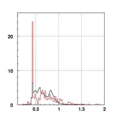
The very first detector built and operated with about 8000 SiPMs from MEPhI/PULSAR is the CALICE hadronic calorimeter prototype for an ILC detector [21, 22]. An example of the characterization studies and selection criteria applied on the MEPhI/PULSAR SiPMs is reported in figure 6. SiPMs are selected with a noise rate of less than 3 kHz at 7.5 pixels threshold, corresponding in this detector to half of the signal of a minimum ionizing particle. Additional requirements on optical crosstalk and SiPM current reduce the yield only slightly. The response and the noise of the SiPM are sensitive to temperature variations. A decrease by one degree leads to a decrease of the breakdown voltage by 50 mV, which is equivalent to an increase of the bias voltage by the same amount. Being the very first mass produced SiPMs, these devices came from various, quite different batches. The operation voltage of each batch has a spread of about 5 V, and the SiPM gains are in the range 0.3-1.3.
The spread of parameters has consequences for the design of the readout electronics. Each SiPM requires individual voltage adjustment with a precision better then 50 mV, and a stability of the supplied power of better then 10 mV. To better cope with the spread in SiPM gain it is desirable to have individual preamplification adjustment for each channel in the readout chip, or individual adjustable zero suppression thresholds. Examples of readout chip architectures are discussed in section 5.
The second generation prototype [22] of the CALICE hadronic calorimeter, is being equipped with CPTA/Photonique SiPMs of the type n-on-p. The test of the first thousand pieces produced shows a significant reduction of dark rate and noise compared to the earlier SiPMs333This is not intended as a comparison of the quality of the two producers, as significant improvement has come from the first experience of MEPhI/PULSAR.. The spread in SiPM gain and in operation voltage remains similar, and with that the implications on the design of the readout electronics.
From the characterization studies of the Hamamatsu MPPC used in the detector for T2K [23] one sees the range of operation voltages is reduced to 3 V, but still too large to remove the requirement of individual voltage adjustment. The SiPM gains for about 17000 devices are in the range 4-5.5 and the dark rate at 0.5 pixel threshold ranges between 300 kHz and 800 kHz. These SiPMs were selected with a failure rate of less then 0.05%.
4.2 Application of SiPMs in calorimetry
As already mentioned the pioneering detector R&D for the application of SiPMs in calorimetry
is the analog hadronic calorimeter (AHCAL) of CALICE [21, 22].
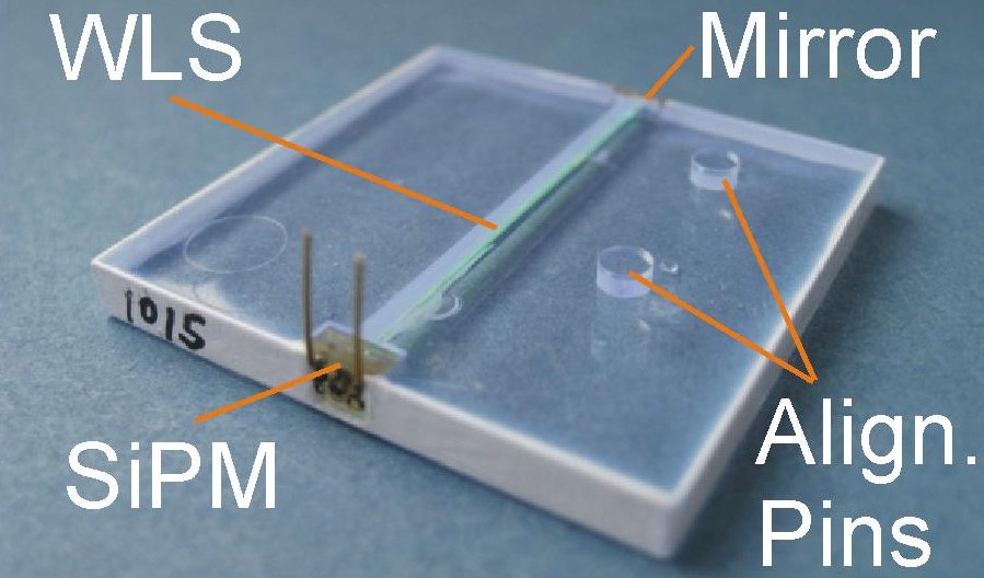
The most recent design for the scintillator tile/SiPM system for this project is shown in figure 7. A plastic scintillator tile (top) of 3.03.00.3 cm3 is read out via a CPTA/Photonique SiPM (796 pixels).
The scintillation light is shifted to the green wavelength and coupled to the photo-detector via a WLS fiber with a mirror at the opposite side of the SiPM.
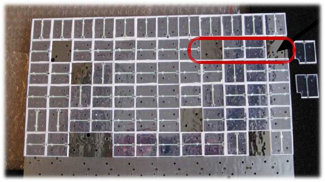
About 150 of these tiles are assembled on the back of one PCB carrying the readout electronics. This constitutes one
calorimeter module (figure 7 bottom).
The alignment of the tiles is ensured by pins realized during the molding of the scintillators.
For each calorimeter module the analog signals from the SiPMs are read out by four 36-channel ASICs, the SPIROC chip. With this design a
calorimeter cell offers a detection efficiency for single minimum ionizing particles of 95% with noise hit probability of 10-4 above threshold.
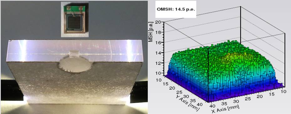
An optimized design of the calorimeter basic unit, the tile, is proposed in [24] (see figure 8), where blue-sensitive SiPMs are directly coupled to plastic scintillators without a WLS fiber. To achieve satisfactory uniformity of response over the tile surface a special shaping of the coupling position has been developed. The new tile geometry is well suited for mass production and shows good overall performance in terms of uniformity and light yield.
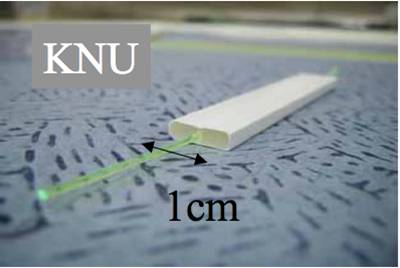
Alternative to the tile shape, mini-strips are a promising solution to increase the effective granularity of plastic scintillator calorimeters even further. The smallest cell size of this kind is designed for the CALICE electromagnetic Tungsten-scintillator sampling calorimeter (ScECAL, [19]). Scintillator strips of size 1.04.50.3 cm3 are manufactured by an extrusion method with a central hole of 1 mm diameter to place the WLS fiber.
Tests have been made with a co-extruded coating of TiO2 (for light shielding), but the uniformity of the light collection along the strip was not satisfactory. The final design adopts reflector foils to optically isolate each individual strip in a detector layer [25].
A similar strip design has been used extensively in several detectors for the T2K experiment.
4.3 Calibration and monitoring system
One of the advantages of using SiPMs in a system is the possibility to calibrate and monitor the gain of the device from the single photoelectron peak spectrum. This requires illuminating each SiPM with low light intensity (1-2 p.e.). As the SiPM gain is sensitive to temperature and voltage changes, monitoring the gain allows to correct for variations in the detector response. The advantage of this method is that it is insensitive to small variations in the light intensity emitted from the light source.
Alternatively, the response of the SiPM can be monitored using a medium light intensity (20-100 p.e.), but in this case the stability of the light intensity has to be ensured either by construction (laser) or via extra monitoring (LED+PIN photo-diode system). For light intensities larger than a few 100 p.e. the effect of the SiPM non-linearity becomes relevant.
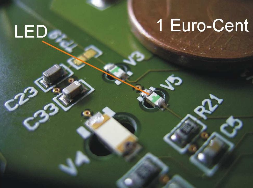
Monitoring the saturation point of the SiPM response function allows to monitor the number of active pixels in the device. This is possibly relevant in case of expected aging due to operation at very high over-voltage or in a hard radiation environment. In this case the light monitoring system has to be capable of delivering a high light intensity, typically a factor 2-3 larger than the number of pixels in the SiPM. Furthermore, the duration of light emission must be small (typically 10 ns) compared to the emission spectrum of the scintillator system. Such requirements are not easy to meet for thousands of channels. Two alternative design concepts are presented in [26], one based on a central driver and optical signal distribution via notched clear fibers, one based on electrical signal distribution and an individual SMD-type LED per calorimeter cell. With both systems single photoelectron peak spectra are nicely obtained, while studies are still ongoing to demonstrate if the SiPM saturation can be monitored.
| Chip name | Measured quantity | Application | Input configuration | Technology |
|---|---|---|---|---|
| FLC_SiPM | Pulse charge | ILC analog HCAL | Current input | CMOS 0.8um |
| MAROC2 | Pulse charge, trigger | ATLAS lumi | Current input | SiGe 0.35um |
| SPIROC | Pulse charge, trigger | ILC HCAL | Current input | SiGe 0.35um |
| NINO | Pulse width, trigger | ALICE ToF | Differential input | CMOS 0.25um |
| PETA | Pulse charge, trigger, time | PET | Differential input | CMOS 0.18um |
| BASIC | Pulse height, trigger | PET | Current input | CMOS 0.35um |
| SPIDER | Pulse height, trigger, time | SPIDER RICH | Current input | |
| RAPSODI | Pulse height, trigger | SNOOPER | Current input | CMOS 0.35um |
| Chip name | N of chan. | Digital | Area [mm2] | Dynamic | Input R [] | Timing |
|---|---|---|---|---|---|---|
| output | range | jitter [ps] | ||||
| FLC_SiPM | 18 | n | 10 | |||
| MAROC2 | 64 | y | 16 | 80 pC | 50 | |
| SPIROC | 36 | y | 32 | 2000 pe | ||
| NINO | 8 | n | 8 | 2000 pe | 20 | 15 |
| PETA | 40 | y | 25 | 8 bit | 50 | |
| BASIC | 32 | y | 7 | 70 pC | 17 | 120 |
| SPIDER | 64 | n | 15 | 12 pC | ||
| RAPSODI | 2 | y | 9 | 100 pC | 20 |
5 SiPM dedicated readout chips
SiPMs are an excellent device for highly granular multi-channel systems. To exploit at best the advantages of SiPMs they need to be read out via a dedicated multi-channel chip. Depending on the specific application few chips have established themselves among the users community. Table 1 shows an overview edited by W. Kucewicz in [28]. A comprehensive list of references to individual publications for each chip can be found in this document.
The table compares eight SiPM-dedicated ASIC chips developed for applications in HEP, medical
physics and homeland security. The chips can be distinguished in two categories according to
the measurements they allow to perform on a given signal from the detector: only energy (either
through a charge measurement, or a pulse height / pulse width measurement), or energy and time.
Furthermore, they have to be distinguished for the output they offer, analog or digital. An already digitized output
has the clear advantage of a simpler and cheaper readout electronics stage after the chip.
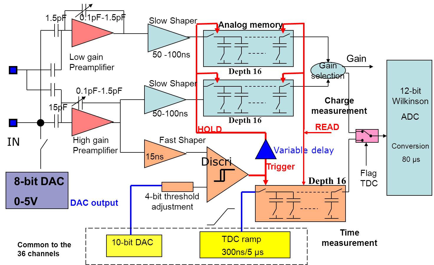
For instance, the main new features of the SPIROC compared to its predecessor, the FLC_SiPM chip
are the integration of the digitization step (12-bit ADC and 12-bit TDC for charge
and time measurements) and the self-triggering capability with an adjustable zero suppression threshold,
which acts as an on-detector zero suppression.
When working with a large number of SiPMs not preselected in terms of operation voltage it is necessary to adjust each bias voltage individually. This is easiest achieved with a programmable DC voltage level added to the SiPM bias line. The SPIROC, FLC_SiPM and SPIDER chips for example provide a DAC-steerable voltage of typically 5 V on each input line for a channel-wise adjustment. An example is shown in figure 11, where the SiPM anode is connected directly to the chip input pin (IN) using an RC filter to ground (not shown) with R=50 and C=100 nF. The voltage generated on the 50 resistor is amplified by an AC-coupled low noise charge sensitive amplifier. The combination of this coupling capacitance and the charge sensitive amplifier results in a voltage readout scheme. In order to fit inside the chip package the coupling capacitor cannot be too large. In this design C=1.5 pF is used for the low gain line and C=15 pF for the high gain line. The effect is that only a small portion of the about 106 electrons generated in one Geiger discharge are effectively measured. For a SiPM gain smaller than 5105 the single photoelectron peak spectra cannot be properly resolved with this method.
Recently new SiPMs with gains of 2.5105 and lower have become available. Hence, a charge sensitive readout scheme is being investigated which could make the SPIROC chip even more versatile in dealing with a large variety of SiPMs. One solution is the use of a current conveyor before preamplification at the same time removing the 50 termination resistor in the voltage scheme. In this approach the bias-tuning DAC voltage is coupled onto the signal line, while the input current is scaled down and sent to the preamplifier. A similar circuit is implemented in the BASIC chip to fine tune the bias voltage for each of the 32 channels.
A variable gain in the chip preamplifier stage compensates the SiPM gain dispersion. The first three chips in the list have programmable preamplifiers, which allow to measure input signals in the range from 1 to 2000 p.e.
For some specific applications, like operation in the dense environment of a sandwich calorimeter at the ILC, ultra-low power consumption is an important issue. The chips in the “ROC” family are designed to operate with pulsed power supply for minimized heat dissipation. The foreseen power consumption amounts to 25 W per channel for the final ILC operation.
6 Conclusions
Silicon Photomultipliers are a novel, yet well established technology for detection of visible photons. They are a very promising alternative to standard photo-multiplier tubes in many applications in high energy physics and also in medical fields. Their small size makes them suitable for the direct single-channel readout of highly segmented detectors, like for example calorimeters, fiber tracking detectors and positron emission tomography detectors. Though the application of SiPMs is rapidly growing and extending to always new designs the mass production capability of these photo-detectors is still not fully proportionate to the request. The physics community recognizes the need of more competitive products commercially available in large quantities and with a minimum spread of the key parameters like operation voltage, gain, dark rate, crosstalk, photo-detection efficiency, etc..
For a detector operating a large number of SiPM a monitoring system is often mandatory. Two possible designs are discussed in which light from an LED is used to monitor the SiPM gain and response, and possibly the saturation point of the SiPM non-linear response function.
To fully exploit the advantages of SiPMs as photo-detectors, newly developed multi-channel readout chips are required. Available chips for SiPM readout are presented and theirs differences and advantages are discussed. To accommodate the large variety of existing SiPMs the ideal readout chip should offer single-channel adjustable voltage, preamplifier gain and/or zero suppression threshold.
7 Acknowledgments
I thank Yuri Musienko, Jelena Ninkovic, Wojtek Kucewicz, from whom I have taken large part of the material needed for this review. Furthermore, I thank my colloages from the CALICE collaboration for allowing me to present material and results from their research. Work supported by the Helmholtz-Nachwuchsgruppen grant VH-NG-206.
References
- [1] http://pc3k40.exp.mephi.ru/.
- [2] J. Ninkovic et al., Nucl. Instr. and Meth. A 610 (2009), p. 142.
- [3] C. Degenhardt et al., proceeding to IEEE NSS-MIC Conference, 2009, Orlando, Florida.
- [4] P. Eckert et al., Nucl. Instr. and Meth. A 620 (2010) p. 217. doi:10.1016/j.nima.2010.03.169.
- [5] http://www.hamamatsu.com.
- [6] http://photonique.ch.
- [7] Y. Musienko, Nucl. Instr. and Meth. A 598 (2009), p. 213.
- [8] A. Lacaita, et al., IEEE Trans. Electron Devices ED-40 (1993), p. 577.
- [9] A. Akindinov, et al., Proceedings of the Eighth ICATPP Conference on Advanced Technology and Particle Physics, Villa Erba, Como, 6-10 October 2003, World Scientific, Singapore, 2004.
- [10] http://www.sensl.com.
- [11] http://www.st.com/.
- [12] Measurements performed by J. Ninkovic.
- [13] http://sipm.itc.it/.
- [14] P. Buzhan et al., ICFA Instrum. Bull. 23 (2001), p. 28.
- [15] W.G. Oldham et al.,IEEE Trans. Electron. Dev. ED-19 (9) (1972), p. 1056.
- [16] B. Dolgoshein, Proceedings of the 42nd Workshop of the INFN ELOISATRON Project, Erice, Italy. Published by World Scientific Publishing Co. Pte. Ltd., (2004), DOI: 10.1142/9789812702951_0029.
- [17] http://www.zecotek.com.
- [18] The International Large Detector: Letter of Intent. Toshinori Abe et al., FERMILAB-LOI-2010-03, FERMILAB-PUB-09-682-E, DESY-2009-87, KEK-REPORT-2009-6, (2010) arXiv:1006.3396. T. Behnke et al., arXiv:0712.2356 (2007).
- [19] D. Jeans, Proceeding for the 13th International Conference on Calorimetry in High Energy Physics (CALOR08), Pavia, Italy, 26-30 May 2008. Published in J.Phys.Conf.Ser.160:012026 (2009).
- [20] Y. Kudenko, proceeding to the 10th International Conference on Instrumentation for Colliding Beam Physics (INSTR08), Novosibirsk, Russia, 28 Feb - 5 Mar 2008. Published in Nucl.Instrum.Meth.A598:289-295,2009.
- [21] C. Adloff et al., JINST 5:P05004, (2010).
- [22] K. Gadow, E. Garutti et al., (2010) EUDET-Report-2010-02, http://www.eudet.org.
- [23] M. Yokoyama et al., Nucl. Instr. and Meth. A 622 (2010) p. 567.
- [24] F. Simon, C. Soldner, C. Joram, proceedings to IEEE NSS-MIC Conference, Knoxville, Tennessee, (30 Oct-6 Nov 2010) arXiv:1011.5033.
- [25] A. Khan, (2010) arXiv:1007.2553.
- [26] P.Göttlicher, proceeding to IEEE NSS-MIC Conference, 2009, Orlando, Florida.
- [27] J. Cvach, M. Janata, J. Kvasnicka, EUDET-Report-07 (2008), http://www.eudet.org/e26/e26/e27/e825/EUDET_report_07.pdf.
- [28] W. Kucewicz, Talk at Industry-academia matching event on SiPM and related technologies, (2011). https://indico.cern.ch/conferenceTimeTable.py?confId=117424#20110216.
- [29] M. Bouchel et al., proceeding to IEEE NSS-MIC Conference, 2008, Dresden, Germany, (19-25 Oct 2008). See also http://omega.in2p3.fr.