Send correspondence to M.Y.: E-mail: mikhail.yurkov@desy.de, Telephone: +49 40 8998 2676
Potential of the FLASH FEL technology for the construction of a kW-scale light source for the next generation lithography111 Submitted to Journal of Micro/Nanolithography, MEMS and MOEMS (JM3)
Abstract
The driving engine of the Free Electron Laser in Hamburg (FLASH) is an L-band superconducting accelerator. It is designed to operate in burst mode with 800 microsecond pulse duration at a repetition rate of 10 Hz. The maximum accelerated beam current during the macropulse is 9 mA. Our analysis shows that the FLASH technology has great potential since it is possible to construct a FLASH like free electron laser operating at the wavelength of 13.5 and 6.8 nanometer with an average power up to 2.6 kW. Such a source meets the physical requirements for the light source for the next generation lithography.
keywords:
Free electron laser, Lithography, Next Generation Lithography, Coherence, VUV radiation, Soft x-ray radiation, x-ray laser1 Introduction
The roadmap for the development of the next generation lithography has been formulated by industry in the middle of the 1990s (see [1, 2] and references therein). A goal was to follow Moore’s law in the reduction of a feature size by a factor of two in two years [3]. During the last two decades the progress in the feature size reduction has been provided by reducing the wavelength of light sources (lasers) used. Now conventional lasers reached their limit. Immersion and photoresist technologies aiming for a feature size below the limit reached their boundaries as well. That is why it was decided to base the next generation lithography (NGL) on a completely new light source – a plasma source producing extreme ultraviolet light at the wavelength of 13.5 nm aiming for a feature size of 20 nm. Microelectronic technology itself contains several challenging technologies inside such as mask, reticle, resist, stepper, etc. Here we discuss only the problem of the light source. 15 years of development of light sources for the NGL allowed to make significant progress, and a 20 W source for a beta-level EUV scanner has been delivered to industry [4]. However, it is generally accepted that the problem of light source for high volume manufacturing (HVM) is not solved yet.
Requirements for the source are not fixed but evolve with the evolution of all the other technologies involved. For instance, requirement for the average power (after intermediate focus (IF), in-band spectrum % around 13.5 nm, etendue of the source output 3 mm2-sr) has been increased nearly by an order of magnitude during the last ten years, and approaches two hundred Watts.
During the last years we observed rapid progress in the development of VUV and x-ray free electron lasers. The jump in the wavelength was about five orders of magnitude, from 12 m in 1997 down to 0.12 nm in 2009 [5, 6, 7, 8, 9, 10, 11]. FLASH (Free Electron Laser in Hamburg) at DESY has produced unprecedented powers of EUV radiation at wavelengths of 13.5 nm and 6.8 nm, target wavelengths for the next generation lithography (NGL) [9, 10]. Several schemes for a dedicated FEL-based radiation source for the NGL have been proposed during last years [12, 13, 14, 15, 16, 17, 18, 19, 20, 21]. In this paper we describe the potential application for the NGL of an accelerator and FEL technology developed in the framework of the FLASH project at DESY. We show that this technology allows to construct a free electron laser operating at the wavelength of 13.5 nm and 6.8 nm with an average power of several kilowatts. This becomes possible due to two main factors. The first one is high average power (about 100 kW) in the electron beam of a superconducting accelerator. The second important factor is undulator tapering allowing significant increase of FEL efficiency above 2%. As a result, high average radiation power of about several kilowatts can be generated. Additional application of the electron beam energy recovery would allow to increase the duty factor significantly such that the average radiation power will be in the multi-ten-kW range [13]. Spectral width of the radiation (below 2%) fits well to the requirements of the radiation source for the Next Generation Lithography.
2 Principle of FEL operation
A free electron laser is a system consisting of a relativistic electron beam and a radiation field interacting with each other while they propagate through an undulator [22]. The undulator is a periodical magnetic structure forcing electrons to perform transverse oscillations. When an electron beam traverses an undulator, it emits radiation at the resonance wavelength . Here, is the undulator period, is the electron beam energy, is the dimensionless undulator strength parameter, is the maximum on-axis magnetic field strength of the undulator, is the relativistic factor, is the velocity of light, and and are charge and mass of the electron, respectively. The electromagnetic wave is always faster than the electrons, and a resonant condition occurs when the radiation slips a distance relative to the electrons after one undulator period. The fields produced by the moving charges in one part of the undulator react on moving charges in another part of the undulator. Thus, we deal with tail-head instability leading to a growing concentration of particles wherever a small perturbation started to occur. More details on FEL physics can be found in ref. [23].
FEL devices can be divided in two classes: amplifiers and oscillators. FELs based on oscillator principle are limited on the short-wavelength side to ultraviolet wavelengths primarily because of mirror limitations. Free electron lasing at wavelengths shorter than ultraviolet can be achieved with a single-pass, high-gain FEL amplifier. The FEL collective instability in the electron beam produces an exponential growth (along the undulator) of the modulation of the electron density on the scale of undulator radiation wavelength. Power gain in excess may be obtained in the short wavelength range. Conversion efficiency of the kinetic energy of electrons to the VUV or soft x-ray radiation can be rather high, up to a few per cent. Average power of the electron beam can be high as well, of the order of a hundred kilowatts. As a results, it becomes possible to generate high average power of the radiation at the level of a few kilowatts. Modern accelerator technologies provide high efficiency of the conversion of the net electric power to the electron beam (of about 10 per cent), thus allowing to obtain net efficiency of FEL on the level of a fraction of per mille. As we already mentioned application of the electron beam recovery may significantly increase the net efficiency.
3 Key elements of the FLASH/TESLA technology
An FEL amplifier starting from the shot noise in the electron beam is a device in which the electron beam produces powerful radiation during single pass through an undulator [24, 25]. This type of devices is frequently referred as Self Amplified Spontaneous Emission FEL (SASE FEL) [26]. Efficient operation of SASE FELs is possible with thorough design of all systems involved. Here we describe the main systems related to the FLASH/TESLA technology.
The TESLA project (TeV Energy Linear Accelerator) has been developed by an international TESLA collaboration since the beginning of the 1990s. More than 50 institutions from 12 countries were involved in the development of superconducting accelerator technology for a high energy electron-positron linear collider and for a driver-linac for an X-ray free electron laser (XFEL) [27, 28]. Later the TESLA Collaboration has been transformed into the TESLA Technology Collaboration (TTC) aiming at technical development for superconducting accelerators, and gave birth to two FEL projects at DESY: FLASH FLASH and the European XFEL [7, 29].
3.1 Main accelerator
All FLASH/TESLA type accelerators are based on superconducting accelerator modules. Each module contains eight superconducting sections. Each section is approximately 1 meter long and operates at a resonance frequency of 1.3 GHz. The accelerating sections are cooled by liquid helium with temperature of 2 K. The accelerating gradient may be different for different sections, and may approach 40 MV/m for the best quality sections. The spread of accelerating gradients is defined by the production technology chain available, and there is clear tendency for improving the quality [30, 31]. Project value for average gradient in the accelerating module for the European XFEL is 24.3 MV/m [32]. Dedicated technological studies are on the way aiming at achieving an average accelerating gradient in excess of 35 MV/m [33]. These developments are performed in the framework of International Linear Collider (ILC) project.
Up to four accelerating modules are powered by one rf station consisting of klystron and modulator [32, 34]. Average and peak power of the klystron are 150 kW and 10 MW, respectively. The accelerator operates in the burst mode. For the FLASH project macropulse repetition rate is 10 Hz, macropulse duration is 1 ms, average beam load within macropulse may reach 10 mA. The total rf pulse length for the European XFEL is 1.37 ms, of which 0.72 ms are required for filling the cavity with rf power, and 0.65 ms for electron beam acceleration. Macropulse repetition rate may be increased for the price of macropulse length reduction. Since the filling time remains the same, higher efficiency of the accelerator is achieved at a reduced repetition rate.
3.2 Laser driven rf gun
The electron beam is produced in a laser driven RF gun[35]. While the linear accelerator is superconducting, the RF gun operates at room temperature. An important figure of merit for the beam quality is the transverse phase space of the electron beam or emittance (it is just the product of the beam size by the angle spread) which should not be much larger than radiation wavelength. The physical parameters related to the quality of the injector is the normalized emittance, . Current values of the normalized emittance achieved in the rf guns produced for FLASH and European XFEL are in the range 0.4 - 1 mm-mrad depending on the bunch charge [36]. These values are sufficient for effective generation of x-ray generation.
3.3 Beam formation system
Effective operation of the VUV/x-ray FEL amplifier requires a high value of the peak beam current of about a few thousand Ampers. The typical value of the peak beam current in the rf gun is about a few tens of Ampers. The required value of the peak beam current is achieved in the beam formation system. During initial stage of amplification the electron bunch is accelerated in an off-crest rf phase and gains energy chirp such that particles in the head of the bunch have less energy. This leads to the compression of the bunch when the electron beam passes through the bunch compressor - a dispersive element providing different path lengths for particles with different energy. Additional installation of rf sections operating at a multiple frequency improves the quality of compressed bunches. Auxiliary sections operating at a frequency of 3.9 MHz are used in FLASH and European XFEL [37]. Two and three bunch compressor stages are implemented in the FLASH and EXFEL accelerators providing peak currents up to 2.5 kA and 5 kA, respectively [29, 38].
3.4 Undulators
Undulators are widely used as insertion devices at synchrotron radiation facilities around the world. The most popular undulators are designed using permanent magnet technology [39, 40]. This technology reached mature level and allows to build undulators with high quality of magnetic field required for FEL applications: relative field errors below per mille level and trajectory errors on a few micron level [11, 29]. Different field geometries (planar or helical) can be realized providing the possibility to generate radiation with required polarization properties (linear or circular). Currently the length of undulator systems at the FEL facilities constitute tens of meters, and exceeds hundred meters for future projects (see Table 1).
4 FLASH facility
The FLASH facility is driven by a superconducting linear accelerator and operates on the DESY site [7, 8, 9, 10]. The aim of this project is to serve as a user facility, and gain experience for the XFEL project realization [29]. The project FLASH started as relatively small test facility accelerator with an energy of 240 MeV passed several upgrades. Currently it consists of 1.2 GeV accelerator and free electron laser operating in the wavelength range from 4.2 nm up to 47 nm [7, 8, 9, 10]. It produces an ultimate peak power on a few GW level, and peak brilliance exceeding by eight orders of magnitude those values obtained from the third generation synchrotron radiation sources. The FLASH facility is equipped with five beam lines for user experiments [43].

A schematic layout of the FLASH facility is shown in Fig. 1. The electron beam is produced in a radio frequency gun and brought up to an energy of up to 1200 MeV by seven accelerating modules ACC1 to ACC7 operating at a frequency of 1.3 GHz. At intermediate energies of 150 and 450 MeV the electron bunches are compressed in the bunch compressors BC1 and BC2. The electron beam formation system is based on the use of linearized longitudinal compression realized with the help of an accelerating module operating at a frequency of 3.9 GHz. After the bunch compressor BC2, the electron beam is accelerated to the target energy (450 to 1200 MeV), and produces powerful coherent radiation during a single pass through the long undulator (planar, hybrid, 12 mm fixed gap, magnetic length 27 m, period 27.3 mm, peak magnetic field 0.48 T).
All subsystems of the superconducting linear accelerator have been optimized for the burst mode of operation with a macropulse repetition rate of 10 Hz, flat-top macropulse duration of 800 s, and maximum beam loading 9 mA within the macropulse. With these parameters the average power in the electron beam is equal to 86 kW at the energy of 1.2 GeV. High power in the electron beam is the main basis for the generation of high EUV radiation power.
Since 2005 FLASH operates as a user facility with high duty factor during user runs: 7 days per week and 24 hours per day [10, 43]. One maintenance shift per week is foreseen for technical service and hardware developments when it is necessary. The operation schedule includes also dedicated runs for technical developments of accelerator and FEL subsystems. One of the tasks which is supported by the program of International Linear Collider is demonstration of reliable operation of the FLASH accelerator with 9 mA beam loading. There is definite progress on this way, and now we can state that this is technically possible [44]. The next step under discussion is to demonstrate lasing at full beam loading. Currently maximum average radiation power has been demonstrated during user runs with small beam load. Macropulse repetition rate was 10 Hz, single-pulse energy was up to 0.2 - 0.3 mJ, the number of pulses per train was up to 100 which corresponds to an average radiation power about 0.2 - 0.3 Watt. At the moment we do not see severe obstacles preventing lasing of full train at full beam load. However, our observation is that the high beam load program will benefit a lot with construction of a dedicated test facility. With FLASH being a user facility with only a small fraction of scientific applications requesting ultimate level of radiation power, the investigation of full power capabilities of the FLASH/TESLA technology is unfortunately limited.
5 European x-ray free electron laser
The internationally organized European X-ray free electron laser (XFEL) is under construction in Hamburg [29]. The construction of the linac is a common effort of many institutes sharing the responsibility for this superconducting linac. The overall coordination is with DESY chairing the XFEL Accelerator Consortium [32]. Main contributions come from CEA Saclay/IRFU, France; CNRS LAL, Orsay, France; DESY, Germany; INFN Milano, Italy; Soltan Institute, Poland; CIEMAT, Spain. The project is the first large scale application of the TESLA technology developed over the last 15 years. Superconducting accelerating cavities will be used to accelerate the electron beam to an energy of up to 17.5 GeV. In a start-up scenario European XFEL will be equipped with three undulator beamlines with total magnetic length of undulators about 450 meters. The facility will cover continuosly wavelength ranges from 0.05 nm to 60 nm.
The accelerator will consist of 100 accelerating modules, i.e. 800 superconducting accelerating structures, operating at a gradient of 24.3 MV/m. A total of 25 RF stations will supply the necessary RF power of typically 5.2 MW per four modules. Construction work along the 3.4 km European XFEL facility started early 2009. Start of the accelerator commissioning is scheduled for 2015. It is important to notice the high level of industrialization of the main components of the accelerator for the European XFEL involving such companies as Thales, Toshiba, CPI, Research Instruments and E. Zanon [32].
6 Dedicated FEL source for NGL
| FLASH | NGL-680 | NGL-1250 | NGL-2500 | |
| Electron energy, MeV | 680 | 680 | 1250 | 2500 |
| Bunch charge, nC | 1 | 1 | 1 | 1 |
| Peak current, A | 2500 | 2500 | 2500 | 2500 |
| Normalized emittance, mm-mrad | 1.5 | 1.5 | 1.5 | 1.5 |
| rms energy spread, MeV | 0.5 | 0.5 | 0.5 | 0.5 |
| Macropulse duration, ms | 0.8 | 0.8 | 0.8 | 0.8 |
| Micropulse rep. rate, MHz | 9 | 10 | 10 | 10 |
| # pulses in macropulse | 7200 | 8000 | 8000 | 8000 |
| Macropulse rep. rate, Hz | 10 | 10 | 10 | 10 |
| Undulator period, cm | 2.73 | 2.73 | 3.7 | 5.0 |
| Undulator length, m | 27 | 30 | 30 | 30 |
| Radiation wavelength, nm | 13.5 | 13.5 | 13.5 | 13.5 |
| FWHM spectrum bandwidth, % | 0.7 | 0.7 | 0.7 | 0.7 |
| Energy in the radiation pulse, mJ | 1.4 | 8.5 | 22 | 33 |
| Peak power, GW | 5.6 | 34 | 88 | 130 |
| FWHM pulse duration, fs | 250 | 250 | 250 | 250 |
| FWHM spot size, mm | 0.17 | 0.3 | 0.2 | 0.1 |
| FWHM angular divergence, rad | 30 | 48 | 54 | 64 |
| Average radiation power, W | 100 | 680 | 1760 | 2640 |


In this section we demonstrate the potential of the FLASH/TESLA tecnology for generation of high average power radiation. First proposals of such kind appeared at an early stage of FLASH/TESLA technology development[13, 45, 46]. Presently this technology reached mature level, and many of the project goals and milestones have been achieved. Moreover, a large scale facility, namely European XFEL, is under construction which is totally based on FLASH/TESLA technology. Nearly all components for this facility are produced by industrial companies, and the next turn is payback of FLASH/TESLA technology to edge technological areas like the Next Generation Lithography. In the present feasibility study we do not deviate much from the project numbers for components used in the FLASH and European XFEL projects. The only principal extension is application of undulator tapering to increase FEL efficiency[47] which already has been used in early proposals of high average power FELs for industrial applications[45, 46]. Recently principle of undulator tapering has been demonstrated experimentally [48, 49].
We assume operation of the linac in the burst mode with macropulse repetition rate of 10 Hz. Macropulse duration is equal to 1 ms. Bunches with a charge of 1 nC are separated by time interval of 100 ns (10 MHz repetition rate) which corresponds to 10 mA beam load within the macropulse. With these parameters average power in the electron beam is equal to 100 kW at the energy of electrons of 1 GeV.
6.1 Operation at the wavelength of 13.5 nm
We consider SASE FEL (single-pass FEL amplifier starting from shot noise in the electron beam) operation. In the following we optimize the SASE FEL operation at the wavelength of 13.5 nm. We assume parameters of the electron beam as given in Table 2. This parameter set is compiled on the base of our experimental experience from FLASH . At an appropriate optimization of the beam formation system we can expect the value of the normalized emittance below 1 mm-mrad. However, a conservative value of normalized emittance of 1.5 mm-mrad is sufficient for effective operation of a 13.5 nm FEL, and we use this number as baseline parameter in this section. We optimize the FEL parameters by varying the energy of the driving electron beam between 625 Mev and 2500 MeV.
The undulator is assumed to be hybrid planar with variable gap. General feature is that shorter gain length is achieved at a shorter undulator period and at smaller undulator gap. In the case under study we deal with high power electron and photon beams, and the matter of concern is to provide sufficient aperture for the transport of both beams. We set the limit on the minimum undulator gap to 1.2 cm like in the FLASH project. We assume the length of the undulator segments to be 200 cm, total magnetic length of the undulator is 30 meters, and focusing beta function is equal to 200 cm. Calculations are performed with the time-dependent simulation code FAST[50].
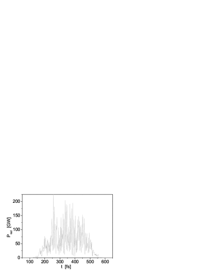
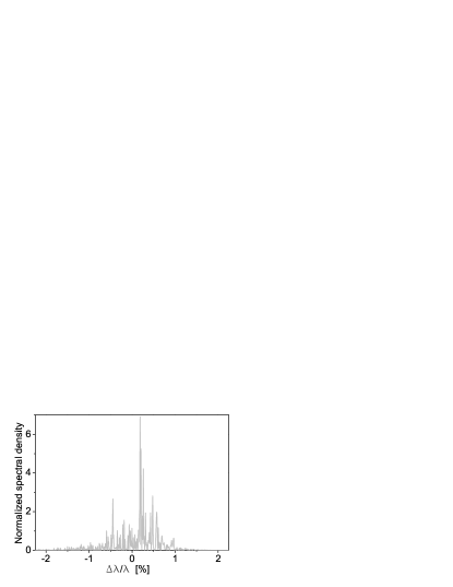
Results of the simulations are shown in Fig. 2. We obtain that within the given parameter space undulator tapering is a very powerful tool for increasing the FEL efficiency, roughly by about a factor of five with respect to the saturation efficiency. The results obtained are very impressive: for a chosen electron energy of 2500 MeV, the average radiation power exceeds 2.5 kW (see Fig. 3). At a reduced electron energy (1250 MeV) we obtain an average radiation power of 1.7 kW. The FEL efficiency is about 1.8% in this case. In conclusion we present the main characteristics of the radiation pulse in Figs. 4 and 5: temporal and spectral properties, intensity distribution at the undulator exit, and angular distribution in the far zone. Note that phase volume of the radiation is nearly diffraction limited, i.e. about radiation wavelength. Spectrum width is also small, and all radiation power goes within ”in-band” requirements for the NGL radiation source.
6.2 Operation at the wavelength of 6.8 nm
| Electron energy, MeV | 1250 | 1250 | 2500 | 2500 |
| Bunch charge, nC | 1 | 1 | 1 | 1 |
| Peak current, A | 2500 | 2500 | 2500 | 2500 |
| Normalized emittance, mm-mrad | 1.5 | 1 | 1.5 | 1 |
| rms energy spread, MeV | 0.5 | 0.5 | 0.5 | 0.5 |
| Macropulse duration, ms | 0.8 | 0.8 | 0.8 | 0.8 |
| Micropulse rep. rate, MHz | 10 | 10 | 10 | 10 |
| # pulses in macropulse | 8000 | 8000 | 8000 | 8000 |
| Macropulse rep. rate, Hz | 10 | 10 | 10 | 10 |
| Undulator period, cm | 3.7 | 3.7 | 5.0 | 5.0 |
| Undulator length, m | 30 | 30 | 30 | 30 |
| Radiation wavelength, nm | 6.8 | 6.8 | 6.8 | 6.8 |
| FWHM spectrum bandwidth, % | 0.7 | 0.7 | 0.7 | 0.7 |
| Energy in the radiation pulse, mJ | 11 | 16 | 20 | 28 |
| Peak power, GW | 44 | 64 | 80 | 110 |
| FWHM pulse duration, fs | 250 | 250 | 250 | 250 |
| FWHM spot size, mm | 0.11 | 0.12 | 0.09 | 0.08 |
| FWHM angular divergence, rad | 35 | 38 | 41 | 41 |
| Average radiation power, W | 880 | 1280 | 1600 | 2240 |


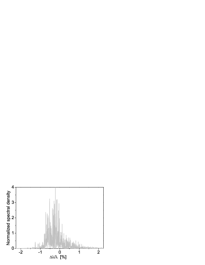


The FEL is tunable radiation source, and there is a simple deal to go over to different wavelength, for instance, to the next target wavelength of 6.8 nm discussed in the NGL community. We restrict our study electron with energies of 1250 MeV and 2500 MeV, and use undulators optimized for generation of 13.5 nm radiation (see previous section). Tuning of the wavelength is performed by the increase of the undulator gap from 12 mm to 18 mm. Magnetic field changes from 1 T to 0.7 T. Evolution of the energy in the radiation pulse is shown in Fig. 6. Comparison of the pulse energies at 6.8 nm and 13.5 nm shows reduction of the pulse energy when going to shorter wavelength. Partially this reduction relates to nonoptimal undulator: period length has been optimized for 13.5 nm. Another factor is reduction of the FEL gain and FEL efficiency due to shorterning of the wavelength. FEL elefficiency can be increased with the reduction of the electron beam emittance. Curves 2 and 4 in Fig. 6 show gain curves of the SASE FEL driven by the electron beam with normalized emittance of 1 mm-mrad. Output power in the case becomes to be comparabable with the case of the wavelength 13.5 nm and mm-mrad. Recent developments of the laser driven rf gun demonstrated feasibility for generation of the beams with rms normalized emittance well below 1 mm-mrad [36]. Thus, we can conclude that it is technically feasible to produce 2 kW level of the average radiation power at the wavelength of 6.8 nm. It is important that the same hardware (accelerator and undulator) is used for production of the radiation with wavelength of 13.5 nm and 6.8 nm. Key parameters of the radiation: temporal and spectral structure of the radiation pulse, intensity distribution of the radiation (see Figs. 7 and 8) do not differ much from characteristics of the source tuned to 13.5 nm (see Figs. 4 and 5).
7 Discussion
Up to now two technologies for the light source are developed by industry: laser produced plasma (LPP), and discharge produced plasma (DPP) [1, 2]. Serious obstacle on the way to a HVM source is the small efficiency of these sources which requires deposition of huge power in a small volume. Another problem is the mitigation of the plasma debris required for the protection of EUV optics. An FEL based radiation source has evident advantages. The process of light generation takes place in vacuum, and there is no problem to utilize the spent electron beam (remove unused power). The problem of debris mitigation does not exists at all. There is no collector problem since the radiation is produced in the diffraction limited volume, and there is no problem with the transport of the radiation to the exposure tool.
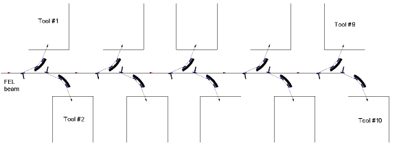
Laser and plasma radiation sources may operate only at a limited set of discrete wavelengths. Each dedicated source operates at a fixed wavelength only. With a SASE FEL driven by 1 - 2 GeV electron beam, the available wavelength range can span from about 100 nm down to a few nanometers. This feature can be helpful for instance, for optimization of a photoresist. It is important that the same hardware (accelerator and undulator) can be used for production of tunable powerful radiation as we demonstrated in our paper. Average power of this ”clean” EUV radiation is in the range of a few kilowatts, an order of magnitude above present requirements for a HVM source. Thus, one FEL set up can replace a dozen of plasma sources. Currently microelectronic industry uses an approach of a single source for a single tool (stepper). In the case of using a powerful FEL as the source we can modify this approach to a single source for multiple tools. We can discuss, for instance, transport of the photon beam to different tools allowing their quasi-simultaneous operation [16, 51, 52] (see Fig. 9). Another option which is under discussion is generation of the radiation in several undulators quasi-simultaneously [17].
The parameter space considered in this conceptual study does not deviate much from project parameters of FLASH/TESLA technology. Main idea was the demonstration of the capabilities of this technology to produce multi-kW level of output radiation power and show that properties of the radiation meet requirements of the Next Generation Lithography. It is important that the described device can be constructed now without additional R&D using components developed for FLASH and European XFEL. Definitely, there is a room for further optimization of the source. This can be essential subject for joint collaboration between R&D departments of microelectronic industry and developers of accelerator and FEL techniques. For instance, it is rather easy to increase average output power of the source by means of increasing the length of macropulse and corresponding reduction of the repetition rate. Alternatively, macropulse repetition rate can be increased for the price of reduction of the output power. This kind of considerations has been already analyzed in the framework of the European XFEL project [29].
Within long term of FLASH/TESLA technology development we can discuss extensions towards increase of duty factor up to cw mode of operation. This activity is also performed in the framework of TESLA Technical Collaboration. One of the problems to be solved is that of high duty cycle or cw injectors generating low emittance beams [53, 54]. The necessary replacement of klystrons by Inductive Output Tubes (IOT) seems to be possible [55]. When the injector technology becomes available, the FEL based radiation source can operate in cw mode. Application of energy recovery will allow to go over to higher output radiation powers.
Acknowledgements
We thank R. Brinkmann for interest in this work and support. We thank O. Gushchin, E. Saldin, and G. Shirkov for their interest in this work. We thank E. Syresin for useful discussions. During the EUVL Symposium in Barcelona and several meetings later on we had the possibility for stimulating discussions with our colleagues from the FEL community and from industry: V. Banine, U. Dinger, A. Endo, A. Goehnermeier, M. Goldstein, M. Kemp, E. Minehara, R. Moors, J.H. Peters, E. Sohmen, U. Stamm, X.J. Wang, and P. Willemse. We also thank V. Bakshi and A. Endo for an invitation to discuss the potential of FELs for the next generation lithography.
References
- [1] Vivek Bakshi (Editor), EUV Sources for Lithography, SPIE Press Monograph, Vol. PM149, 2006.
- [2] Vivek Bakshi (Editor), EUV Lithography, SPIE Press Book, Vol. PM178, 2008.
- [3] Gordon E. Moore, Electronics, Volume 38, Number 8, April 19, 1965.
- [4] Vivek Bakshi, EUV Sources Come Back as Top EUV Lithography Concern, Semiconductor International, July, 2009. http://www.semiconductor.net. http://www.euvlitho.com/2011/2011
- [5] M. Hogan et al., Phys. Rev. Lett. 81, p. 4867, 1998.
- [6] S.V. Milton et al., Science, 292, p. 2037, 2001.
- [7] T. Åberg, et al., A VUV FEL at the TESLA Test Facility at DESY, Conceptual Design Report, DESY Print TESLA-FEL 95-03 , May 1995.
- [8] J. Andruszkow et al., Phys. Rev. Lett. 85, p.3825, 2000.
- [9] W. Ackermann et al., Nature Photonics, 1, p. 336, 2007.
- [10] S. Schreiber et al., Proc. FEL2010, Malmo, Sweden, 2010, TUOBI2. http://accelconf.web.cern.ch/AccelConf/FEL2010/papers/tuobi2.pdf.
- [11] P. Emma et al., Nature Photonics, 4, p. 641, 2010.
- [12] Brian E. Newnam, Proc. SPIE, Vol. 1343, p. 214, 1991.
- [13] C. Pagani et al., Nucl. Instrum. and Methods A 463, p.9, 2001.
- [14] G. Dattoli et al., Nucl. Instrum. and Methods A 474, p.259, 2001.
- [15] M. Goldstein et al., Proc. 27th FEL Conference, Stanford, p. 422, 2005.
- [16] E.L. Saldin, E.A. Schneidmiller, H. Weise, and M.V. Yurkov, Free electron laser as a potential source for EUV lithography, talk at the EUVL Source Workshop, Barselona, 2006.
- [17] E. Minehara et al., A multi-kW EUV light source driven by energy-recovery linac, talk at the EUVL Source Workshop, Barselona, 2006.
- [18] E.L. Saldin, E.A. Schneidmiller, V.F. Vogel, H. Weise and M.V. Yurkov, Proc. FEL2009, Liverpool, UK, MOPC54. http://accelconf.web.cern.ch/AccelConf/FEL2009/papers/mopc54.pdf.
-
[19]
E. Syresin et al.,
Proc. RuPAC-2010, Protvino, Russia, 2010.
http://accelconf.web.cern.ch/AccelConf/r10/papers/wepsb003.pdf. - [20] E.M. Syresin et al., Journal of Surface Investigation. X-ray, Synchrotron and Neutron Techniques, 5, p.520, 2011.
- [21] Y. Socol, G.N. Kulipanov, A.N. Matveenko, O.A. Shevchenko, and N.A. Vinokurov, Phys. Rev. ST Accel. Beams 14, p.040702, 2011.
- [22] E.L. Saldin, E.A. Schneidmiller, and M.V. Yurkov, Free-Electron Lasers, (in: Springer Handbook of Lasers and Optics, Chapter 11 (Springer, New York, 2007), pp. 814-819.
- [23] E.L. Saldin, E.A. Schneidmiller, and M.V. Yurkov, The Physics of Free Electron Lasers (Springer-Verlag, Berlin, 1999).
- [24] Ya.S. Derbenev, A.M. Kondratenko, and E.L. Saldin, Nucl. Instrum. and Methods 193, p.415, 1982.
- [25] J.B. Murphy and C. Pellegrini, Nucl. Instrum. and Methods A 237, p.159, 1985.
- [26] R. Bonifacio, F. Casagrande and L. De Salvo Souza, Phys. Rev. A 33, p.2836, 1986.
- [27] Conceptual Design of 500 GeV e+e- Linear Collider with Integrated X-ray Facility (Edited by R. Brinkmann et al.), DESY 1997-048, ECFA 1997-182, Hamburg, May 1997.
-
[28]
TESLA Technical Design Report, DESY 2001-011, March 2001
http://tesla.desy.de/new_pages/0000_TESLA_Project.html. - [29] Altarelli, M. et al. (Eds.), XFEL: The European X-Ray Free-Electron Laser, Technical Design Report. Preprint DESY 2006-097, DESY, Hamburg, 2006 (see also http://xfel.desy.de).
- [30] L. Lilje and D. Reschke, Proc. LINAC08 Conference, Canada, THP014. http://accelconf.web.cern.ch/AccelConf/LINAC08/papers/thp014.pdf.
- [31] W. Singer et al., Proc. IPAC’10 Conference, Kyoto, Japan, 2010, THOARA02. http://accelconf.web.cern.ch/AccelConf/IPAC10/papers/thoara02.pdf.
- [32] H. Weise, Proc. Linear Accelerator Conference LINAC2010, Tsukuba, Japan, MO102. http://accelconf.web.cern.ch/AccelConf/LINAC2010/papers/mo102.pdf.
- [33] N. Ohuchi et al., Proc. IPAC’10 Conference, Kyoto, Japan, 2010, WEPE008. http://accelconf.web.cern.ch/AccelConf/IPAC10/papers/wepe008.pdf.
- [34] S. Choroba, Proc. PAC07 Conference, Albuquerque, New Mexico, USA, 2007, TUXC03. http://accelconf.web.cern.ch/AccelConf/p07/PAPERS/TUXC03.PDF.
- [35] S. Rimjaem et al., Proc. EPAC08 Conference, Genoa, Italy, 2008, MOPC078. http://accelconf.web.cern.ch/AccelConf/e08/papers/mopc078.pdf.
- [36] S. Rimjaem et al., Proc. IPAC’10 Conference, Kyoto, Japan, 2010, TUPE011. http://accelconf.web.cern.ch/AccelConf/IPAC10/papers/tupe011.pdf.
- [37] E. Vogel et al., Proc. IPAC’10 Conference, Kyoto, Japan, 2010, THPD003. http://accelconf.web.cern.ch/AccelConf/IPAC10/papers/thpd003.pdf.
- [38] I. Zagorodnov and M. Dohlus, Phys. Rev. ST Accel. Beams 14, p. 014403, 2011.
- [39] H. Onuki and P. Elleaume, Undulators, Wigglers, and Their Applications (Taylor Francis, New York 2003).
- [40] J. Pflueger, Nucl. Instrum. and Methods A 445, p. 366, 2000.
- [41] C.J. Bocchetta et al., FERMIElettra CDR, Synchrotrone Trieste, 2007, http://www.elettra.trieste.it/FERMI.
- [42] T. Tschentscher, Layout of X-Ray Systems, Europena XFEL Technical Note XFEL.EU TN-2011-001.
- [43] K. Tiedtke et al., New J. Phys. 11, 023029, 2009.
- [44] S. Pei et al., Proc. IPAC’10 Conference, Kyoto, Japan, 2010, TUPEA059. http://accelconf.web.cern.ch/AccelConf/IPAC10/papers/tupea059.pdf.
- [45] C. Pagani, E.L. Saldin, E.A. Schneidmiller and M.V. Yurkov, Nucl. Instrum. and Methods A 423, p. 190, 1999.
- [46] C. Pagani, E.L. Saldin, E.A. Schneidmiller and M.V. Yurkov, Nucl. Instrum. and Methods A 455, p.733, 2000).
- [47] N. Kroll, P. Morton, M. Rosenbluth, IEEE J. Quant. Electr. 17, p.1436, 1981.
- [48] Y. Hidaka et al., Proc. 2001 Part. Acc. Conference, New York, USA, 2011, THP148, http://www.c-ad.bnl.gov/pac2011/proceedings/papers/thp148.pdf.
-
[49]
D. Ratner et al.,
Proc. FEL2009, Liverpool, UK, TUOA03.
http://accelconf.web.cern.ch/AccelConf/FEL2009/papers/tuoa03.pdf. - [50] E.L. Saldin, E.A. Schneidmiller, and M.V. Yurkov, Nucl. Instrum. and Methods A 429, p.233, 1999.
- [51] E.L. Saldin, E.A. Schneidmiller, and M.V. Yurkov, Nucl. Instrum. and Methods A 507, p.510, 2003.
- [52] E.L. Saldin, E.A. Schneidmiller, and M.V. Yurkov, The Potential for the Development of the X-Ray Free Electron Laser, DESY Print TESLA-FEL 2004-02, Hamburg, 2004.
- [53] A. Arnold et al., 14th SRF Conference, Berlin, p.20, 2009.
- [54] T. Kamps et al., 14th SRF Conference, Berlin, p.164, 2009.
- [55] Y. Li, EUROFEL-Report-2007-DS5-074.