Unraveling of free carrier absorption for terahertz radiation in heterostructures
Abstract
The relation between free carrier absorption and intersubband transitions in semiconductor heterostructures is resolved by comparing a sequence of structures. Our numerical and analytical results show how free carrier absorption evolves from the intersubband transitions in the limit of an infinite number of wells with vanishing barrier width. It is explicitly shown that the integral of the absorption over frequency matches the value obtained by the f-sum rule. This shows that a proper treatment of intersubband transitions is fully sufficient to simulate the entire electronic absorption in heterostructure THz devices.
pacs:
78.67.Pt,78.40.Fy,73.40.Kp,85.35.BeI Introduction
The absorption of electromagnetic radiation due to the interaction with electrons in bulk crystals is essentially determined by two distinct effects: (i) The free carrier absorption (FCA), which is directly related to the electrical conductivity and drops with frequency on the scale of the inverse scattering time. (ii) Interband transitions, which are typically described via the dipole moments induced by the coupling between states in different bands. For most crystals these transition energies are of the order of eV and thus this dominates the response around the optical spectrum. In addition to these electronic features, optical phonons provide absorption in the far infrared region, which is not addressed here.
Semiconductor heterostructures provide an additional effective potential for the electron in the conduction band causing a further quantization of the electronic states in the growth direction (denoted by ). Taking into account the degrees of freedom for motion in the plane, this establishes subbands within the conduction band. Commonly, the absorption between these subbands is treated analogously to the interband transitions in bulk crystals. The standard treatment relies on the envelope functions for the subbands with energies and areal electron densities using expressions for the absorption coefficient as Helm (1999); Ando (1978)
| (1) |
where and the counter-rotating terms are neglected. Here is the elementary charge, is the refractive index, and is the vacuum permeability (SI units are used). The matrix element
| (2) |
describes the coupling strength. Throughout this work we assume the polarization of the electric field to point in -direction and that the wave propagates in a waveguide of effective thickness which is filled by the (layered) semiconductor material. This scheme is also routinely applied for the calculation of the gain spectrum of quantum cascade lasers (QCLs).Faist et al. (1994) In this context the broadening can be either added in a phenomenological way Ajili et al. (2006) or by detailed calculations, see, e.g., Ref. Unuma et al., 2003. It can also be seen as a limiting case of a full quantum kinetic calculation.Wacker et al. (2009)
While the conventional treatment of intersubband transitions is well accepted for transitions in the infrared, this approach is less obvious for THz systems, which have become of high interest.Williams (2007); Lee and Wanke (2007) Here, FCA-related features might turn up as a strong competing mechanism to the intersubband gain transition in analogy to the bulk case where both FCA and interband transitions occur as separate processes. In order to demonstrate the potential relevance, we consider the standard expression for FCA in bulk systemsYu and Cardona (1999)
| (3) |
where is the effective mass, the volume density of electrons in the conduction band, and is the scattering time. As an example for GaAs with a doping of and ps (corresponding to a mobility of 6000 cm2/Vs at 300K Meyer and Bartoli (1987)) one obtains for a frequency THz. This is larger than typical gain coefficients in THz quantum cascade lasers.Jukam et al. (2009); Martl et al. (2011); Burghoff et al. (2011) Thus, bulk FCA would provide a strong obstacle in achieving lasing in such structures and its proper treatment in heterostructures is of crucial importance for the description of QCLs or other THz heterostructure devices. (For a typical infrared laser, in contrast, it was shown that FCA in the cascade structure does not play a role.Giehler et al. (2004)) In Ref. Ajili et al., 2006 FCA was only considered in the waveguide layers but not the QCL structure itself, where the absorption was determined by intersubband transitions. Furthermore, in Ref. Vurgaftman and Meyer, 1999 it was shown that processes as described by Eq. (1) dominate the absorption of light (with -polarized electric field) for quantum wells.
In this context the question arises how such a treatment based on intersubband transitions is related to the FCA in the bulk. Is FCA related to the seemingly dominating intersubband processes or does it stem from further processes not identified yet? In the latter case, such processes could strongly alter the THz performance of heterostructure devices. In order to shed light on this important issue we present a detailed study on the unfolding of FCA starting from different types of heterostructure. Our main conclusion is that the absorption due to intersubband transitions evolves into the bulk FCA for vanishing barrier widths. This shows that a proper treatment of intersubband transitions provides a complete description of gain and absorption processes in heterostructure devices.
II From superlattice to bulk
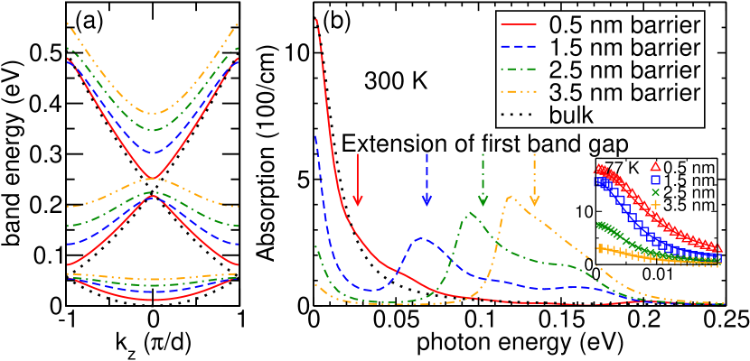
We consider four GaAs-Al0.3Ga0.7As superlatticesGrahn (1995) (SLs) with constant period nm. The barrier width is set equal to 0.5 nm, 1.5 nm, 2.5 nm, and 3.5 nm, respectively, and a homogeneous doping with is used. The sample with the 2.5 nm barrier has been investigated in Ref. Helm et al., 1993, which motivates our choice. Fig. 1(a) shows the calculated minibands assuming effective masses of and for GaAs and Al0.3Ga0.7As, respectively, where is the free electron mass, as well as a conduction band offset of 276 meV.Vurgaftman et al. (2001) Further information on the structures is given in table 1.
| barrier width (nm) | 0.5 | 1.5 | 2.5 | 3.5 |
| miniband width (meV) | 42.7 | 25.4 | 15.6 | 10.1 |
| effective mass | 0.071 | 0.090 | 0.125 | 0.178 |
| at 300 K (A/Vcm) | 11.2 | 6.4 | 2.4 | 0.8 |
| at 77 K (A/Vcm) | 17 | 14.9 | 7.3 | 2.9 |
Here the zero-field conductivity is evaluated from the nonequilibrium Green’s function (NEGF) model following Ref. Lee et al., 2006; *NelanderDiss2009, which includes scattering processes from phonons, impurities, interface roughness (with an average height of one monolayer and a length correlation of 10 nm), and alloy disorder in an approximate way. This program also calculates the absorption in linear response to the optical field Wacker et al. (2009) as given in Fig. 1(b). Using the conductivity for the 0.5 nm barrier structure provides a scattering time of fs. This value agrees roughly with the momentum scattering rate ps (which is the sum of the elastic and inelastic scattering rateWacker (2002)) extracted from several highly doped GaAs/AlAs SLs with narrow barriers at room temperature.Schomburg et al. (1998) This value is much smaller than the bulk scattering time of 0.2 ps, as scattering is enhanced due to the presence of rough interfaces in all SLs (which are particular strong scatterers for small barrier widths, when the wave functions highly penetrate through the barriers). In addition, the assumption of a constant scattering time is only expected to be of semi-quantitative nature, the same holds for the approximations in matrix elements used. (For a more detailed treatment of roughness scattering in thin barriers, see Ref. Carosella et al., 2010.) Using fs, the Drude expression (3) fits the absorption quite well, demonstrating, that these small barriers actually provide almost the bulk free carrier absorption behavior.
With increasing barrier thickness the conductivity becomes smaller due to the reduced coupling between the quantum wells. Accordingly, there is a decrease in the low frequency absorption
| (4) |
as it follows from electrodynamics.Jackson (1998) Here our numerical calculations are in full agreement, as we do not employ the rotating wave approximation and include broadening in a fully consistent way. Furthermore, for thicker barriers, the absorption between the minibands becomes more prominent and thus the absorption increases close to the photon energy required to overcome the gap between the first and the second miniband, as indicated by the arrows in Fig. 1(b). The shift of the peak positions with respect to the minigaps can be related to scattering induced level shifts. For the 2.5 nm barrier the results are in good agreement with the measurements reported in Ref. Helm et al., 1993. The onset of absorption around 100 meV is slightly sharper in the experiment, which may be attributed to less rough interfaces or to the limited accuracy of the various approximations used for the scattering potentials.
For SLs the absorption can be understood within the common miniband picture. For low frequencies intra-miniband processes dominate, which are easily treated in semiclassical transport models providing for zero electric fieldKtitorov et al. (1972); Ignatov et al. (1993)
| (5) |
This behavior was experimentally observed in Refs. Brozak et al., 1990; Tamura et al., 1999. Here, for large miniband widths. With decreasing miniband width, the increase of reduces . An even stronger reduction arises, if the miniband width drops below either or the Fermi energy, see Ref. Wacker, 2002 for details.111The sequential tunneling picture provides similar results for Wacker (2002). Thus no major differences are expected for thick barriers For all superlattice structures studied by our NEGF model, we found good agreement with (5) for low frequencies. Some examples are shown in the inset of Fig. 1(b). As a further example, the calculated absorption spectrum at 65 K for the structure of Ref. Tamura et al., 1999 can be fitted by ps (not shown here). This is in good agreement with the experimental value of 0.18 ps, which demonstrates the quality of the NEGF approach.
For higher frequencies, transitions between the minibands can describe the absorption between 60 and 200 meV very well. See, e.g., the results of the calculations in Ref. Helm et al., 1993, which fully agree with our more sophisticated NEGF approach.
We conclude that the absorption of SLs at zero bias can be well described by the Drude-like miniband conduction result (5) for low frequencies and by common inter-miniband transitions for higher frequencies. As shown in Fig. 1(b), the combination of both features evolves into the bulk FCA (3) if the barrier width becomes small.
III From multiple well to superlattice
Now we want to study, how the SL absorption arises from the behavior of systems containing few wells, which show distinct absorption peaks between discrete levels. Fig. 2 shows the absorption for multi-quantum-well structures, as presented in Fig. 2(a) for the case of two wells. Here, all parameters correspond to the SL with a 1.5 nm barrier discussed above. For the double well structure, essentially the two lowest subbands are occupied in thermal equilibrium, and one observes clear absorption peaks corresponding to the separations between the subbands, see Fig. 2(b). As the dipole matrix element (2) vanishes for equal parity of the states, not all possible transitions are visible. The observed peak structure can be directly described by the standard intersubband expressions (1). Furthermore, there is zero absorption in the limit of zero frequency as no dc current along the structure is possible, compare Eq. (4).
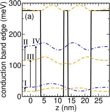
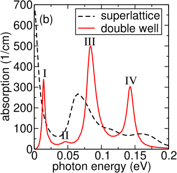
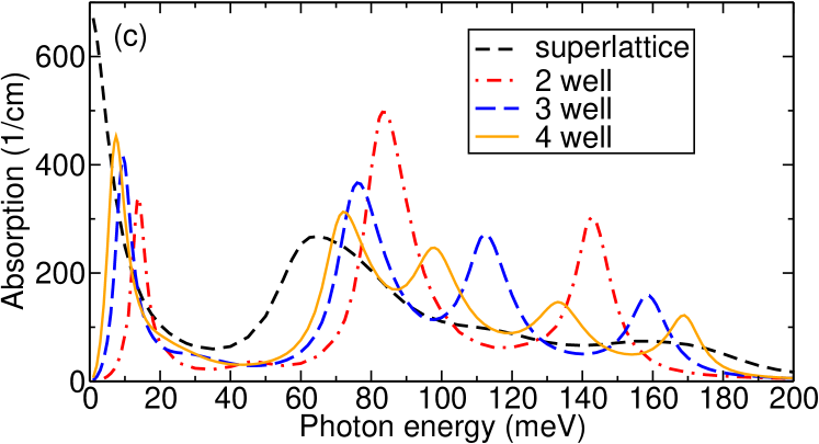
With increasing well numbers, the peaks III and IV of the double well split up and form the continuous absorption between 60 and 200 meV due to the transitions between the first and the second SL miniband, see Fig. 2(c). While this is quite expected, peak I does not show any clear splitting, but shifts to lower frequencies, approaching the intra-miniband absorption. This behavior can be understood by a detailed study of the multi-quantum-well eigenstates. Here, a tight binding model for wells with next neighbor coupling shows (see the appendix A for details): (i) There are eigenstates, labeled by an index according to their energy . Here is of the order of . (ii) The matrix element from Eq. (2) is small unless for neighboring states, i.e. . Thus, the transitions between neighboring states dominate, explaining the strong absorption around visible in Fig. 2(c), where essentially corresponds to the miniband width of the infinite structure. Together with a tail at higher frequencies due to broadening of these transitions this explains the appearance of the Drude-like miniband absorption for the SL in the limit of large . For the evolution is not smooth as any finite sequence of quantum wells has a zero dc conductivity in contrast to an infinite SL and thus the absorption must vanish according to Eq. (4).
IV The integrated absorption
Summing over all possible intersubband transitions (1), we obtain the total absorption . Here the discrete index runs over all (infinitely many) eigenstates of the heterostructure of finite length, including states which correspond to unbounded states with energies far above the barrier potential. Integrating over all frequencies provides
| (6) |
under the assumption – otherwise the counter-rotating terms become of relevance, which had been neglected here. In appendix B we show that the same integral relation is more generally obtained for arbitrary level spacings within our NEGF model, which also covers dispersive gain.Terazzi et al. (2007); Wacker (2007)
Following Ref. Peeters et al., 1993, Eq. (6) can be simplified by the Thomas-Reiche-Kuhn sum ruleKuhn (1925); *ReicheZP1925 (also called f-sum ruleMahan (1990)) which reads for a parabolic band with effective mass
and provides the integrated absorption
| (7) |
where is the average three-dimensional carrier density in the waveguide.
For a bulk semiconductor, the free carrier absorption (3) provides after integration over energy
| (8) |
which fully agrees with the intersubband result (7) for equal total densities . Thus the total FCA in a bulk semiconductor equals the total intersubband absorption within the conduction band for a finite heterostructure of finite length, which shows the direct relation between these. More generally, Eqs. (7,8) establish a general rule for the integrated absorption within the conduction band of a semiconductor under conditions, where the approximation of a constant effective mass is justified. In this context superlattices appear as an intermediate case, where the inter-miniband absorption and the Drude-like intra-miniband absorption add up to the full result.Peeters et al. (1993)
Our numerical data in Fig. 1(b) exhibit the integrated absorption for all curves. The data from Fig. 2 provide , where the additional factor takes into account the undoped region of 6 nm between adjacent multiple quantum wells ( is the number of well/barrier combinations with a length of 10 nm each). These values are slightly below the value of given by Eq. (8) using the GaAs effective mass. This minor discrepancy of less than 7% can be easily attributed to some absorption at higher frequencies and the impact of the barrier material with a larger mass.222Indeed we found a consistent change with the barrier thickness: The maximal value of was obtained for the 0.5 nm barrier and the minimal value of for the 3.5 nm barrier in Fig. 1(b). We conclude, that the absorption obtained by our NEGF code is in excellent agreement with the rule (7).
More generally the effect of the semiconductor heterostructure can be understood as shifting the absorption strength within the frequency space, as explicitly demonstrated by our calculations. This perception has actually been used in the design of QCL structures, where the unavoidable free carrier absorption is deflected from the frequency region of operation by a proper choice of heterostructures Faist , see, e.g., Ref. Walther et al., 2006.
V Conclusion
We demonstrated how the common bulk free carrier absorption evolves from standard intersubband absorption in heterostructures for electromagnetic waves with an electric field pointing in growth direction. Here the well-studied SL absorption constitutes an intermediate case, which can be entirely understood on the basis of common intersubband absorption processes in the limit of a growing number of quantum wells. For decreasing SL barrier width the combination of inter- and intra-miniband absorption evolves into the standard FCA of the bulk crystal. This behavior reflects a redistribution of absorption strength, while the integrated absorption is constant. The most relevant consequence is that there is no need to bother about any additional FCA-related absorption processes, provided all intersubband transitions are properly taken into account. A consistency check for the calculated gain/absorption spectrum is whether Eq. (4) is satisfied in the low frequency limit and the integrated absorption matches Eqs. (7,8).
Acknowledgements.
We thank J. Faist for helpful discussions. Financial support from the Swedish Research Council (VR) and the French ANR agency (ROOTS project) is gratefully acknowledged.Appendix A Analytical calculation for coupled wells
We consider a multi-quantum-well structure with wells centered at , where . The ground state of the isolated well has the wavefunction and the energy . Restricting to a nearest neighbor coupling (which is negative for the lowest subband), the eigenenergies are
| (9) |
and the eigenstates read with
If the overlap between the states in different wells is negligible, i.e. , we find , which can be directly evaluated. If is even we find as both states have the same parity with respect to . For odd , some algebra yields
For we thus have:
As the square of enters the absorption (1), it becomes clear that the transitions with highly dominate the absorption spectrum. The energy difference of the corresponding states (9) for these transitions is less than with an average of approximately .
Appendix B Total absorption with the Green’s function model
Here we refer to the formulation of our NEGF model as outlined in Ref. Wacker et al., 2009. Here gain is evaluated within linear response around the stationary state characterized by the Green’s functions . In order to simplify the analysis, nondiagonal are neglected here – they are, however, fully included in our numerical implementation. Then the absorption resulting from the pair of states can be written as
| (10) |
which is essentially the last equation of the appendix in Ref. Wacker et al., 2009 with the counter-rotating term added. Inserting the spectral functionHaug and Jauho (1996) and its occupied part333In thermal equilibrium we have , where is the Fermi-Dirac distribution. , which is assumed to be real, we find
| (11) |
The terms provide the physical origin of dispersive gain as sketched in Refs. Wacker, 2007; Wacker et al., 2009. The signs of the counter-rotating terms seem to contradict our intuition, as the first one appears to relate to emission and the second to absorption. However, in this formulation the sign is defined via the difference in energy between the initial and the final state, where only one a specific combination is used in the prefactor .
Using the general relations
integration of the terms from Eq. (11) over frequency provides
| (12) |
so that the sum over all different pairs equals the second line of Eq. (6). Thus the integrated absorption (7) also holds for the more involved absorption terms (11) of the NEGF model which include the dispersive gain.
References
- Helm (1999) M. Helm, in Intersubband Transitions in Quantum wells, Semiconductors and Semimetals, Vol. 62, edited by H. Liu and F. Capasso (Elsevier, 1999) pp. 1 – 99.
- Ando (1978) T. Ando, J. Phys. Soc. Japan 44, 765 (1978).
- Faist et al. (1994) J. Faist, F. Capasso, D. L. Sivco, C. Sirtori, A. L. Hutchinson, and A. Y. Cho, Science 264, 553 (1994).
- Ajili et al. (2006) L. Ajili, G. Scalari, M. Giovannini, N. Hoyler, and J. Faist, J. Appl. Phys. 100, 043102 (2006).
- Unuma et al. (2003) T. Unuma, M. Yoshita, T. Noda, H. Sakaki, and H. Akiyama, J. Appl. Phys. 93, 1586 (2003).
- Wacker et al. (2009) A. Wacker, R. Nelander, and C. Weber, Proc. SPIE 7230, 72301A (2009).
- Williams (2007) B. S. Williams, Nature Phot. 1, 517 (2007).
- Lee and Wanke (2007) M. Lee and M. C. Wanke, Science 316, 64 (2007).
- Yu and Cardona (1999) P. Y. Yu and M. Cardona, Fundamentals of Semiconductors (Springer, Berlin, 1999).
- Meyer and Bartoli (1987) J. R. Meyer and F. J. Bartoli, Phys. Rev. B 36, 5989 (1987).
- Jukam et al. (2009) N. Jukam, S. S. Dhillon, D. Oustinov, J. Madéo, J. Tignon, R. Colombelli, P. Dean, M. Salih, S. P. Khanna, E. H. Linfield, and A. G. Davies, Appl. Phys. Lett. 94, 251108 (2009).
- Martl et al. (2011) M. Martl, J. Darmo, C. Deutsch, M. Brandstetter, A. M. Andrews, P. Klang, G. Strasser, and K. Unterrainer, Opt. Express 19, 733 (2011).
- Burghoff et al. (2011) D. Burghoff, T.-Y. Kao, D. Ban, A. W. M. Lee, Q. Hu, and J. Reno, Appl. Phys. Lett. 98, 061112 (2011).
- Giehler et al. (2004) M. Giehler, H. Kostial, R. Hey, and H. T. Grahn, J. Appl. Phys. 96, 4755 (2004).
- Vurgaftman and Meyer (1999) I. Vurgaftman and J. R. Meyer, Phys. Rev. B 60, 14294 (1999).
- Grahn (1995) H. T. Grahn, ed., Semiconductor Superlattices, Growth and Electronic Properties (World Scientific, Singapore, 1995).
- Helm et al. (1993) M. Helm, W. Hilber, T. Fromherz, F. M. Peeters, K. Alavi, and R. N. Pathak, Phys. Rev. B 48, 1601 (1993).
- Vurgaftman et al. (2001) I. Vurgaftman, J. R. Meyer, and L. R. Ram-Mohan, J. Appl. Phys. 89, 5815 (2001).
- Lee et al. (2006) S.-C. Lee, F. Banit, M. Woerner, and A. Wacker, Phys. Rev. B 73, 245320 (2006).
- Nelander (2009) R. Nelander, Lineshape in Quantum Cascade Lasers - Temperature, Screening and Broadening, Ph.D. thesis, Lund University (2009).
- Wacker (2002) A. Wacker, Phys. Rep. 357, 1 (2002).
- Schomburg et al. (1998) E. Schomburg, T. Blomeier, K. Hofbeck, J. Grenzer, S. Brandl, I. Lingott, A. A. Ignatov, K. F. Renk, D. G. Pavel’ev, Y. Kosc hurinov, B. Y. Melzer, V. M. Ustinov, S. V. Ivanov, A. Zhukov, and P. S. Kop’ev, Phys. Rev. B 58, 4035 (1998).
- Carosella et al. (2010) F. Carosella, R. Ferreira, G. Strasser, K. Unterrainer, and G. Bastard, Phys. Rev. B 82, 033307 (2010).
- Jackson (1998) J. D. Jackson, Classical Electrodynamics, 3rd ed. (John Wiley & Sons, New York, 1998).
- Ktitorov et al. (1972) S. A. Ktitorov, G. S. Simin, and V. Y. Sindalovskii, Sov. Phys.–Sol. State 13, 1872 (1972), [Fizika Tverdogo Tela 13, 2230 (1971)].
- Ignatov et al. (1993) A. A. Ignatov, K. F. Renk, and E. P. Dodin, Phys. Rev. Lett. 70, 1996 (1993).
- Brozak et al. (1990) G. Brozak, M. Helm, F. DeRosa, C. H. Perry, M. Koza, R. Bhat, and S. J. Allen, Phys. Rev. Lett. 64, 3163 (1990).
- Tamura et al. (1999) K. Tamura, K. Hirakawa, and Y. Shimada, Physica B 272, 183 (1999).
- Note (1) The sequential tunneling picture provides similar results for Wacker (2002). Thus no major differences are expected for thick barriers.
- Terazzi et al. (2007) R. Terazzi, T. Gresch, M. Giovannini, N. Hoyler, N. Sekine, and J. Faist, Nature Physics 3, 329 (2007).
- Wacker (2007) A. Wacker, Nature Physics 3, 298 (2007).
- Peeters et al. (1993) F. M. Peeters, A. Matulis, M. Helm, T. Fromherz, and W. Hilber, Phys. Rev. B 48, 12008 (1993).
- Kuhn (1925) W. Kuhn, Zeitschrift für Physik A Hadrons and Nuclei 33, 408 (1925).
- Reiche and Thomas (1925) F. Reiche and W. Thomas, Zeitschrift für Physik A Hadrons and Nuclei 34, 510 (1925).
- Mahan (1990) G. D. Mahan, Many-Particle Physics (Plenum, New York, 1990).
- Note (2) Indeed we found a consistent change with the barrier thickness: The maximal value of was obtained for the 0.5 nm barrier and the minimal value of for the 3.5 nm barrier in Fig. 1(b).
- (37) J. Faist, Private communication.
- Walther et al. (2006) C. Walther, G. Scalari, J. Faist, H. Beere, and D. Ritchie, Appl. Phys. Lett. 89, 231121 (2006).
- Haug and Jauho (1996) H. Haug and A.-P. Jauho, Quantum Kinetics in Transport and Optics of Semiconductors (Springer, Berlin, 1996).
- Note (3) In thermal equilibrium we have , where is the Fermi-Dirac distribution.