Bloch–Zener Oscillations in Graphene and Topological Insulators
Abstract
We show that superlattices based on zero-gap semiconductors such as graphene and mercury telluride exhibit characteristic Bloch–Zener oscillations that emerge from the coherent superposition of Bloch oscillations and multiple Zener tunneling between the electron and hole branch. We demonstrate this mechanism by means of wave packet dynamics in various spatially periodically modulated nanoribbons subject to an external bias field. The associated Bloch frequencies exhibit a peculiar periodic bias dependence which we explain within a two-band model. Supported by extensive numerical transport calculations, we show that this effect gives rise to distinct current oscillations observable in the - characteristics of graphene and mercury telluride superlattices.
pacs:
72.80.Vp, 73.21.Cd, 85.35.Ds, 85.75.MmI Introduction
Bloch oscillations, the periodic motion of particles in a superlattice subject to a constant external field, represent a fundamental phenomenon in transport through periodic potentials. Predicted already in the early days of quantum mechanics Bloch1929 ; Zener1934 , Bloch oscillations have been observed in various fields of physics, ranging from earlier experiments in semiconductor superlattices Feldmann1992 ; Leo1992 ; Waschke1993 via cold atoms in optical lattices BenDahan1996 ; Wilkinson1996 to classical optical Pertsch1999 ; Morandotti1999 and acoustic Sanchis-Alepuz2007 waves. While many aspects of conventional Bloch oscillations can be explained by a single band description, particularly interesting effects arise in the case of two coupled minibands Fukuyama1973 energetically separated from further bands. Then partial Zener tunneling at avoided crossings of the two minibands can lead to a coherent superposition of Bloch oscillations Rotvig1995 ; Hone1996 , i.e. to a splitting, followed by as subsequent recombination of a Bloch oscillating wave packet. This gives rise to a variety of Rabi-type interference phenomena, in particular double-periodic motions coined Bloch–Zener (BZ) oscillations Breid2006 ; Breid2007 ; Abumov2007 . Signatures of this effect have already been detected in the THz emission of AlGaAs superlatices Shimada2004 , and even the population dynamics have been measured recently for light Dreisow2009 and atomic matter waves Kling2010 in especially tailored binary lattices.
However, materials with a linear Dirac spectrum Wallace1947 naturally serve the effect, since only a small gap is opened by a spatially periodic modulation allowing for Zener tunneling between electron and hole states. Such materials are now at hand with the discovery of graphene Novoselov2004 ; Zhang2005 and the advent of topological insulators Kane2005 ; Kane2005_2 ; Bernevig2006 ; Bernevig2006_2 first realized in two-dimensional mercury teluride (HgTe) heterostructures Koenig2007 ; Roth2009 . Interesting phenomena for graphene based periodic superstructures have already been theoretically predicted like the formation of extra Dirac cones Park2008 ; Barbier2010 ; Brey2009 and the appearance of a negative differential conductance Ferreira2011 . Furthermore, recent experiments have realized graphene superlattices with periodicities down to a few nm Meyer2008 .
This raises the question for the existence of peculiarities of Bloch oscillations in graphene and topological insulator superlattices that we address in this manuscript. We are not aware of work showing unconventional features in graphene-based Bloch oscillations. Up to now, only the semiclassical approach was adapted to a linear dispersion Dragoman2008 and, without reference to Bloch oscillations numerical evidence for a negative differential conductance was reported Ferreira2011 . We show that besides conventional Bloch oscillations, multiple Zener tunneling between the coupled electron and hole branches leads to distinct BZ oscillations that appear to be naturally present in superlattices made of systems with Dirac-like dispersion.
This paper is structured as follows: In Section II we show the influence of BZ oscillations on the wave packet motion in a graphene nanoribbon and the influence on the frequency spectrum. Subsequently, we introduce in Section III a two-band model to explain the effect in the frequency spectrum and the influence of BZ oscillations on the electron-hole polarization. In Section IV we show, that the occurrence of BZ oscillations can be seen as distinct features in the current through graphene nanoribbons. In Section V we present results that feature the special frequency pattern of BZ oscillations, as well as their signatures in transport, in nanoribbons made of the topological insulator mercury telluride.
II Wave-packet motion in graphene superlattices
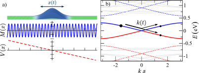
An insight into the dynamics of BZ oscillations can be gained by the time-evolution of a wave packet on a graphene nanoribbon in presence of a periodic mass potential and a linear electrostatic drift potential as sketched in Fig. 1(a). To this end we model the electronic structure of graphene by a conventional tight-binding Hamiltonian Nakada1996
| (1) |
where denotes neighbouring unit cells and the sublattice degree of freedom. The initial wave packet is created by diagonalizing the periodic Hamiltonian of one unit-cell of the infinite ribbon. By means of the transversal eigenfunctions we create an initial electron-like wave packet
| (2) |
with a Gaussian broadening . Since the armchair boundary mixes the two graphene valleys the wavefunction comprises several nodes in lateral direction. The time-evolution is calculated by an expansion of the time-evolution operator in Chebychev polynomials krueckl2009 . In presence of a periodic mass potential
| (3) |
where is the strength of the periodic mass, and the periodicity length, the bandstructure of the superlattice exhibits a small anti-crossing at and a large bandgap between the first and the higher Bloch bands as shown in Fig. 1(b). In presence of the a linear drift potential
| (4) |
with as the strength of the drift field, the wave packet starts to accelerate. Because of its extent in the longitudinal direction, the wave packet is localized in momentum space with a distinct average momentum in -direction. Given the periodicity of the bandstructure, a sawtooth behavior of is obtained known as Bloch oscillations.
However, the dynamics in a graphene nanoribbon shows additional features due to the strong coupling between electron and hole states. Therefore we study a typical trajectory
| (5) |
of the center-of-mass (COM) as shown in Fig. 2(a).
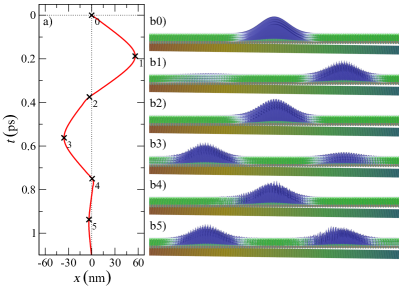
Initially, the wave packet is chosen electron like and a snapshot of the probability distribution is shown in Fig. 2(b0). During the first Bloch cycle the probability distribution is predominantly to the right of the initial position [see Fig. 2(b1)]. This region features a negative electrostatic potential and accordingly the part of the wave packet with electron character performs Bloch oscillations in this region. In Fig. 2(b2) the electron and hole parts meet again in momentum space and as a consequence tunneling from the electron to the hole branch is possible as sketched by the bullets in Fig. 1(b). As a result the hole-like part of the wave-packet increases and in subsequent time steps the COM trajectory reaches negative values. The corresponding snapshot at the turning point of the the wavefunction in Fig. 2(b3) shows a big hole-like state on the left side and a smaller electron-like state on the right side. After the next tunneling the probability distribution between electron and hole states is almost equal, thus the COM motion is strongly suppressed. Because of the periodic mass potential, the gaps between the first Bloch band and higher bands is bigger than the gap between electron and hole states as shown in Fig. 1(b). As a result the tunneling into higher bands is very unlikely and there is no damping of the oscillations due to leakage into higher bands.
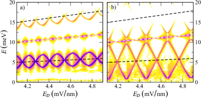
To study the dynamics of the tunneling between the electron and the hole branch in more detail we perform a frequency analysis of the COM motion for different fields . The Fourier amplitudes of the dominant frequency contributions are visualized by dark colors in Fig. 3. Besides the conventional Bloch frequency marked by a white dashed line, the resulting spectrum shows a pronounced interweaving pattern around half of this frequency (black dashed line). A stronger periodic potential, and thereby an increased gap between electron and hole branch, leads to a rhombic structure as shown in Fig. 3(b). These periodic features in the frequency spectrum arise from the interplay between Bloch oscillations and the splitting of the wave packet into the electron and hole branches at (see Fig. 1(a)). The persistent sequence of tunneling events between the two branches and the subsequent interference leads to a new set of frequencies which can be unterstood by means of the following model.
III Analytical model for BZ oscillations
In the following we quantitatively explain these characteristic BZ features using a periodically modulated one-dimensional Dirac model Hamiltonian,
| (6) |
Here is the period, is the Fermi velocity and the energy gap between the electron and the hole states. The resulting bandstructure is given by
| (7) |
as shown in Fig. 4(a). A comparison with the full tight-binding calculation of the graphene nanoribbon in Fig. 1(b) shows a very good correspondence.
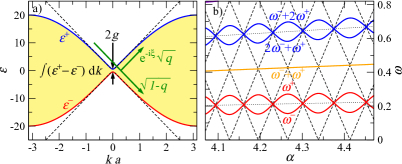
An external electric drift field enters the equations of motion for the quasi-momentum as leading to a time evolution of linear in where . Conventional Bloch oscillations with frequency arise from the periodicity of in momentum space in the interval . The phase between the two branches accumulated during one oscillation is given by a free propagation and thus
| (8) |
with
| (9) |
the area in momentum space as depicted in Fig. 4(a). This free propagation can be expressed by the matrix
| (10) |
Additional to conventional Bloch oscillations on either branch, there is a strong periodic tunneling between the electron and the hole states close to the anti-crossing at . There, the Hamiltonian (6) can be linearized [dashed lines in Fig. 4(a)], leading to a typical Landau–Zener tunneling problem Landau1932 ; Zener1932 ; Stueckelberg1932 :
| (11) |
The scattering between the different branches is described by
| (12) |
with the tunneling rate , , and is an additional tunneling phase. From this we can deduce the scattering matrix
| (13) |
which describes the time-evolution of the electron and hole branch for one Bloch cycle. Using this matrix we derive scattering eigenstates
| (14) |
with the corresponding eigenvalues where
| (15) |
The phases of the scattering eigenstates depend periodically on the phase difference between electron and hole branch. This periodicity leads to two new Bloch frequencies
| (16) |
Unlike conventional Bloch oscillations these frequencies do not simply depend linearly on the drift strength , but show a rapid interweaving pattern strongly changing with , as shown in Fig. 4(b), owing to coherences from combined dynamics on the hole and electron branch. The limiting cases can be understood as follows. For strong coupling, the tunneling rate leads to a frequency [dotted line in Fig. 4(b)], since for every Bloch cycle the states tunnel completely between the two branches in momentum space and hence the complete cycle in position space is twice as long. In the opposite, weak coupling limit leading to a rhombic frequency pattern shown as dashed lines in Fig. 4(b). For intermediate tunneling rates the frequencies show a smooth transition between these limiting cases and are in very good agreement with the numerically calculated spectra of Fig. 3(a,b).
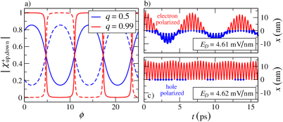
Furthermore, the scattering eigenstates show a strong polarization dependence (electron or hole type character) on the phase , Eq (8). If the one-dimensional model Hamiltonian (6) is considered for , the tunneling rate , which results in strongly electron or hole polarized states for almost all values of . The absolute value of the spinor entries is always very close to one or zero as shown in Fig. 5(a). Nevertheless, the polarization breaks down whenever the difference between the phase of the electron and hole branch is
| (17) |
where . This alternating weight of the spinor between the electron and hole type states for different drift fields can be also deduced from the COM motion of wave packets with fixed initial polarization. If the drift field is adjusted such that the phase condition (17) is approximately satisfied, the COM motion of the initially electron-like configuration exhibits oscillations ranging from to for as shown in Fig. 5(b). Since conventional Bloch oscillations in a single band are restricted to positive or negative values the trajectories imply strong tunneling between the electron and hole states. For values of where condition (17) is not fulfilled, e.g. in Fig. 5(c), the trajectories of the different polarizations do not significantly cross the origin, thus they preserve their electron-hole character. As a consequence, if charge transport through a system comprises a transition from electron to hole states the current should strongly depend on the BZ oscillations within the superstructure.
IV Transport in graphene-based superlattices
In the following, we consider charge transport through graphene nanoribbon based superlattices and demonstrate that BZ oscillations lead to clear-cut features in the - characteristics.
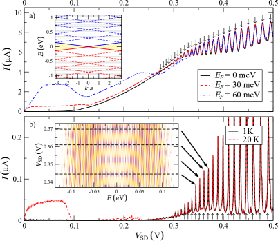
To this end we model a graphene nanoribbon of width and length by the tight-binding Hamiltoninan of Eq. (1), now with a periodic electrostatic potential leading to a superlattice mini-bandstructure as shown in the inset of Fig. 6(a). A small constant mass term is additionally considered which opens up a gap commonly present in experiments on graphene nanoribbons Han2010 . We assume a linear potential drop due to the source-drain voltage between the graphene leads at . The current is calculated by means of the Landauer-Büttiker formalism Buettiker1985 ,
| (18) |
with the Fermi functions .
As shown in Fig. 6, the current through the nanoribbon is governed by a conventional increase with the bias window for small , followed by a region of negative differential conductance typical for superlattices. At higher bias, , we observe the emergence of distinct current oscillations that get more pronounced with increasing gap size, see Fig 6(b). Due to the bias between source and drain electrode the particles traversing the superlattice must change their electron-hole character. However, states performing BZ oscillations exhibit transitions between the two carrier types only for certain when the phase fulfills the condition of Eq. (17) as shown in the previous section. In consequence the current is strongly enhanced if this is fulfilled. As shown in Fig. 6(a,b) the current peaks calculated by Eq. (18) perfectly coincide with the expected voltages (marked by vertical arrows) deduced by extracting the area in momentum space from the minibandes around the Fermi energy shown as shaded area in the inset of Fig. 6(a). Vice versa, the experimental observation of BZ peaks in the - characteristics would allow for ‘measuring’ the miniband structure.
A closer look at the transmission values [see inset Fig. 6(b)] reveals a rhombic structure which features pronounced transmission maxima piled up at these particular values of (dashed lines). Since these maxima are present for various energies in the conductance window, the resulting current is fairly independent of the exact Fermi energy [see Fig. 6(a)] and temperature [see Fig. 6(b)].
V BZ oscillations and transport in HgTe-based superlattices
A different setup featuring BZ oscillations can be created from a strip etched out of the two-dimensional topological insulator based on mercury teluride (HgTe) Koenig2007 ; Roth2009 . We describe the electronic properties of the underlying HgTe heterostructure by the Hamiltonian Bernevig2006
| (19) |
where , , and . We assume an HgTe/HgCdTe heterostructure with a quantum well width of featuring topological edge states and leading to material parameters , , , as typically used in literature Koenig2008 . As for the graphene nanoribbon we can create two different types of superlattices with a mass-like modulation and an electrostatic modulation. For a HgTe strip the mass modulation can be achieved by modulating the width of the ribbon, for example by
| (20) |
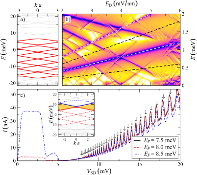
where and are the maximum and minimum width and is the periodicity. The finite width of the HgTe nanoribbon allows for a hybridization of the edge states with the same spin at the opposite boundaries leading to a small gap in the bandstructure Zhou2008 ; krueckl2011 . Accordingly, the modulation of the width corresponds to a modulation of the mass gap. The resulting miniband structure from the two-dimensional system, shown in Fig. 7(a), is obtained numerically by Lanczos diagonalization and exhibits various Landau-Zener anticrossings within the bulk bandgap of HgTe which suggest BZ oscillations.
In order to study the electron dynamics we calculate the COM motion of Gaussian shaped edge-state wave packets. Initially, the wave packet is localized on one edge and the direction of motion is determined by its spin. The array of multiple constrictions enables tunneling between the edges. As a consequence an inversion of the direction of motion is possible, leading to Bloch and BZ oscillations. As shown in Fig. 7(b), the resulting frequency spectrum features the expected rhombic pattern in between the frequencies of the conventional Bloch oscillations (white dashed lines). Compared to the graphene system [see Fig. 3(e)] we observe more complicated, superimposed structures because of the whole sequence of multiple anticrossings in the band structure that affect BZ oscillations.
As for graphene we further study the transport properties of HgTe strips of constant width and a periodically modulated electrostatic potential resulting in a supercell bandstructure shown in the inset of Fig. 7(c). The small gap between the electron and the hole states is attributed to the finite ribbon width of . We chose the Fermi energy close to the band crossing of the topological edge states and calculate the current using Eq. (18). Besides a strong negative-differential conductance at lower bias we get the signatures of BZ oscillations for as shown in Fig. 7(c). Similar to the calculations for the graphene superlattice the oscillations are independent of the exact choice of the Fermi level. The peak positions are in good accordance with the expected series of drift voltages marked by arrows in Fig. 7(c) obtained from Eq. (17), where is extracted from the bands around the Fermi-energy shown as shaded area in the inset.
VI Conclusion
In this manuscript we showed that Bloch–Zener oscillations appear naturally in superlattices made of materials with a Dirac-like spectrum, highlighting interference between electron and hole states. The characteristics of these oscillations are explained by a one-dimensional model Hamiltonian and numerically confirmed for realistic setups by means of wave packet simulations for graphene and topological insulator ribbons. Furthermore, we demonstrated that Bloch–Zener oscillations manifest themselves as regular sequence of pronounced current peaks in quantum transport, besides the well know negative differential conductance at low bias, a signature of conventional Bloch oscillations. The sequence of current peaks associated with the Bloch–Zener oscillations are intimately linked to the underlying miniband structure.
We suggest transport measurements through graphene nanoribbons and HgTe strips as promising experimental setups that feature Bloch–Zener oscillations. For single layer graphene and topological insulators, the periodic electrostatic potential can be imprinted by an array of top gates. The gap between the electron and hole states can be tuned by the width of the considered nanoribbons. In case of bilayer graphene the gap can also be created via a potential difference in -direction induced by top gating. The calculations presented here have been performed for clean, disorder free and coherent systems. However, preliminary numerical calculations for graphene-based superlattices with disorder indicate that Bloch–Zener oscillations are still visible if the mean-free-path exceeds several periods of the superlattice. This is promising with respect to their experimental detection in sold-state based samples.
We finally note that signatures of the Bloch–Zener oscillations presented have been recently observed with ultracold, fermionic K-atoms due to the Dirac points with small mass gaps emerging in tunable optical honeycomb lattices Tarruell2012 .
Note added in proof. Recently, we became aware of Ref. 47 where the Bloch-Zener oscillations of collective excitations in narrow zigzag-shaped optical lattices is studied theoretically.
Acknowledgements.
This work is supported by Deutsche Forschungsgemeinschaft (GRK 1570 and joined DFG-JST Forschergruppe Topological Electronics). We thank T. Hartmann, F. Tkatschenko and D. Ryndyk for useful conversations.References
- (1)
- (2) F. Bloch, Z. Phys. A 52, 555 (1929).
- (3) C. Zener, Proc. R. Soc. Lond. A 145, 523 (1934).
- (4) J. Feldmann et al., Phys. Rev. B 46, 7252 (1992).
- (5) K. Leo et al., Solid State Communications 84, 943 (1992).
- (6) C. Waschke et al., Phys. Rev. Lett. 70, 3319 (1993).
- (7) M. Ben Dahan et al., Phys. Rev. Lett. 76, 4508 (1996).
- (8) S. Wilkinson et al., Phys. Rev. Lett. 76, 4512 (1996).
- (9) T. Pertsch et al., Phys. Rev. Lett. 83, 4752 (1999).
- (10) R. Morandotti et al., Phys. Rev. Lett. 83, 4756 (1999).
- (11) H. Sanchis-Alepuz, Y. Kosevich, and J. Sánchez-Dehesa, Phys. Rev. Lett. 98, 134301 (2007).
- (12) H. Fukuyama, R. Bari, and H. Fogedby, Phys. Rev. B 8, 5579 (1973).
- (13) J. Rotvig, A.-P. Jauho, and H. Smith, Phys. Rev. Lett. 74, 1831 (1995).
- (14) D. Hone and X.-G. Zhao, Phys. Rev. B 53, 4834 (1996).
- (15) B. Breid, D. Witthaut, and H. Korsch, New J. Phys. 8, 110 (2006).
- (16) B. Breid, D. Witthaut, and H. Korsch, New J. Phys. 9, 62 (2007).
- (17) P. Abumov and D. W. L. Sprung, Phys. Rev. B 75, 165421 (2007).
- (18) Y. Shimada, N. Sekine, and K. Hirakawa, Appl. Phys. Lett. 84, 4926 (2004).
- (19) F. Dreisow et al., Phys. Rev. Lett. 102, 076802 (2009).
- (20) S. Kling, T. Salger, C. Grossert, and M. Weitz, Phys. Rev. Lett. 105, 215301 (2010).
- (21) P. Wallace, Phys. Rev. 71, 622 (1947).
- (22) K. Novoselov et al., Science 306, 666 (2004).
- (23) Y. Zhang, Y.-W. Tan, H. Stormer, and P. Kim, Nature 438, 201 (2005).
- (24) C. Kane and E. Mele, Phys. Rev. Lett. 95, 226801 (2005).
- (25) C. Kane and E. Mele, Phys. Rev. Lett. 95, 146802 (2005).
- (26) B. Bernevig, T. Hughes, and S.-C. Zhang, Science 314, 1757 (2006).
- (27) B. Bernevig and S.-C. Zhang, Phys. Rev. Lett. 96, 106802 (2006).
- (28) M. König et al., Science 318, 766 (2007).
- (29) A. Roth et al., Science 325, 294 (2009).
- (30) C.-H. Park et al., Nat. Phys. 4, 213 (2008).
- (31) M. Barbier, P. Vasilopoulos, and F. Peeters, Phys. Rev. B 81, 075438 (2010).
- (32) L. Brey and H. Fertig, Phys. Rev. Lett. 103, 046809 (2009).
- (33) G. J. Ferreira, M. N. Leuenberger, D. Loss, and J. C. Egues, Phys. Rev. B 84, 125453 (2011).
- (34) J. Meyer, C. Girit, M. Crommie, and A. Zettl, Appl. Phys. Lett. 92, 123110 (2008).
- (35) D. Dragoman and M. Dragoman, Appl. Phys. Lett. 93, 103105 (2008).
- (36) K. Nakada, M. Fujita, G. Dresselhaus, and M. Dresselhaus, Phys. Rev. B 54, 17954 (1996).
- (37) V. Krueckl and T. Kramer, New J. Phys. 11, 093010 (2009).
- (38) See Supplemental Material at ??? for a video of Bloch–Zener oscillations on a graphene superlattice.
- (39) L. D. Landau, Phys. Z. Sowjetunion 2, 46 (1932).
- (40) C. Zener, Proc. R. Soc. Lond. A 137, 696 (1932).
- (41) E. C. G. Stueckelberg, Helv. Phys. Acta 5, 369 (1932).
- (42) M. Han, J. Brant, and P. Kim, Phys. Rev. Lett. 104, 056801 (2010).
- (43) M. Büttiker, Y. Imry, R. Landauer, and S. Pinhas, Phys. Rev. B 31, 6207 (1985).
- (44) M. König et al., J. Phys. Soc. Jpn. 77, 031007 (2008).
- (45) B. Zhou, H. Z. Lu, R. L. Chu, S. Q. Shen, and Q. Niu, Phys. Rev. Lett. 101, 246807 (2008).
- (46) V. Krueckl and K. Richter, Phys. Rev. Lett. 107, 086803 (2011).
- (47) L. Tarruell, D. Greif, T. Uehlinger, G. Jotzu, and Tilman Esslinger, Nature 483, 302–305 (2012).
- (48) E. Arévalo and L. Morales-Molina, EPL 96, 60011 (2011).