Microwave-Enhanced hopping-conductivity; a non-Ohmic Effect
Abstract
Hopping conductivity is enhanced when exposed to microwave fields (Phys. Rev. Lett., 102, 206601, 2009). Data taken on a variety of Anderson-localized systems are presented to illustrate the generality of the phenomenon. Specific features of these results lead us to conjecture that the effect is due to a field-enhanced hopping, which is the high frequency version of the non-Ohmic effect, well known in the dc transport regime. Experimental evidence in support of this scenario is presented and discussed. It is pointed out that existing models for non-Ohmic behavior in the hopping regime may, at best, offer a qualitative explanation to experiments. In particular, they cannot account for the extremely low values of the threshold fields that mark the onset of non-Ohmic behavior.
pacs:
72.80.Ng 73.50.Fq 72.20.EeI Introduction
Non-Ohmic effects are commonly encountered in hopping conductivity. Actually, it is difficult to maintain linear-response conditions in these systems. The degree of non-Ohmicity could be tamed by reducing the potential drop across the sample but the need to ensure good signal-to-noise makes this harder as the temperature gets lower. Deviations from linear response may be expected when the applied field obeys:
| (1) |
Here, is Boltzmann constant; e is the electron charge, and the temperature. is the spatial scale over which the electron gains energy from the field before it is dissipated into the bath, usually by phonon emission, and therefore is a function of temperature, typically of the form ( is a number between 1to 4 depending on the material, temperature range, and dimensionality). Modifications to the conductance by a sufficiently large dc field were studied by several, somewhat different theoretical approaches 1 ; 2 ; 3 ; 4 . These models however predicted a similar result; the field induces an excess conductance that, at intermediate field-strength, is exponential with ()γ with =1 or 2. Intermediate fields are fields in the range: . The high-field limit (where the conductance becomes independent of temperature 4 ; 5 ), is defined by , where is the localization length.
Much less attention has been given to the effect of a long-wavelength electromagnetic radiation on hopping conductivity. Of particular interest is where the wavelength is larger than the sample-size 6 which can be readily implemented by using microwaves (MW) radiation. Ben-Chorin et al observed that exposing the sample to a MW source enhanced its hopping conductance and, perhaps naturally, associated the effect with heating 7 . However, systematic studies, exploiting some unique properties of electron-glasses 8 , suggested that this is a non-equilibrium effect. A persistent feature of the results, which made it difficult to reconcile the effect with heating, is a sub-linear dependence of on the microwaves power .
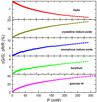
In this paper we report on results obtained by similar measurements on films of five different hopping systems; granular-aluminum, InO (crystalline indium-oxide), InO (amorphous indium-oxide), beryllium, and GaAs. In all cases at 4K turns out to be sub-linear with the MW power in agreement with the results of previous studies. It is further shown that the functional dependence of is consistent with the current-voltage characteristics measured independently (at low frequency) on the same samples. The MW-enhanced conductance is then conjectured to be a non-Ohmic effect, of a similar nature as the field assisted-hopping phenomenon. This is a generic mechanism and should be obeyed by any system once driven away from its linear response transport regime.
As a further test of our conjecture, the temperature dependence of the MW-induced is shown to be in qualitative agreement with models for field assisted hopping. On the other hand, a quantitative analysis of these non-Ohmic effects exposes a discrepancy between these theories and experiments. This discrepancy, well documented in experiments on hopping systems, manifests itself as a much higher sensitivity to fields than suggested by equation 1. It is also pointed out that the exponential dependence on the field, anticipated by theory, might hold only over a very small range of fields.
II Experimental
Several materials were used to prepare samples for measurements in this study. These were thin films of InO and InO, and granular-aluminum. Samples from these materials were prepared by e-gun evaporation of InO or aluminum pellets unto room temperature glass substrates in partial oxygen pressures of (4-6)10-5 mbar and rates of (0.3-1) Å/s. The InO samples were obtained from the as-deposited amorphous films by crystallization at 525 K. We also used for comparison samples of GaAs and beryllium that were highly resistive and exhibited hopping conductance at liquid helium temperatures.
Conductivity of most of the samples was measured using a two terminal ac technique employing a 1211-ITHACO current preamplifier and a PAR-124A lock-in amplifier. The GaAs specimen however, was configured for a Van-der-Pauw, 4-terminal ac measurement. In either case, the ac voltage bias was kept small enough to minimize deviations from Ohmic conditions (as will be shown below, some deviation may be observed even at the smallest fields used).
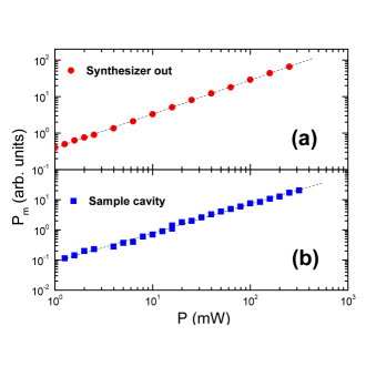
The high-power synthesizer HP8360B, was used with power up to 25 dBm (316 mW) for the MW excitation. The frequency range used in this work was limited to 2-6 GHz. The output of the synthesizer was fed to the sample chamber via a coaxial cable ending with a short antenna. An important issue in the study is the functional form of the sample response to the power of the MW. It was therefore desired to ascertain the linearity of the synthesizer setting versus its output as well as the integrity of the transmission line itself. This was done by measuring the generated power near the instrument output and near the sample stage. The results shown in figure 1 seem to rule out the possibility that the sub-linearity is an instrumental artifact.
Some auxiliary measurements described below employed the Tabor WS8101, a 100 MHz generator as the radio-frequency (RF) source. The output of this generator was inserted into the sample cavity through the same transmission line as the MW source. The linear relation between the setting of the generators and the induced RF voltages across the sample was ascertained by monitoring the pick-up waveforms on an oscilloscope. The data shown in this paper are plotted with respect to the output settings of the respective RF or MW source.
In both the MW and RF experiments an initial frequency scan was made to locate a range where the response is conveniently large. Naturally that was usually one of the resonances of the chaotic cavity in which the sample was mounted. As will be shown below, the positions of these resonances was stable over many hours, and reproducible results could be obtained with a barely noticeable drift in frequency (0.1%/day).
Unless otherwise mentioned, measurements reported here were performed at 4.1K with the sample immersed in liquid helium. Complementary details of sample preparation, characterization, and measurements techniques are given elsewhere 9 .
III Results and discussion
The most characteristic feature of the MW-enhancement phenomenon is the functional form of the excess conductance versus the radiation power . In more than 150 samples studied in our laboratory, increased with less than linearly. Results of scans, illustrating the sub-linear form of the response, are shown in figure 2. The sub-linearity in these results are typical; cases where the sub-linearity was less prominent than those in figure 2 were encountered usually only in samples where the maximum effect was smaller than 2 %.
While linearity at power levels smaller than measured here cannot be ruled out, it is noted that there are instances where is sub-linear at a power such that 10-2. This was the first indication that the origin of the effect is not consistent with ‘heating’; from the point of view of power-balance, a spatially uniform increase of the electron temperature will perforce give when both and are small as is evidently the case for 10-2. An even stronger evidence against ‘heating’ was given in 8 based on the lack of change in the ’memory-dip’ shape upon exposure to MW radiation. The memory-dip is an identifying feature of intrinsic electron-glasses. It is a cusp-like modulation observable in conductance versus gate voltage sweeps 10 . It has a shape that is highly sensitive to the electron temperature and thus may be used a thermometer (see 10 for details). The underlying mechanism for the MW-enhanced conductivity was not identified in 10 .
As more data became available, a statistical correlation emerged between the sensitivity of to the voltage employed in the conductance measurement, and the magnitude of produced by a given power of MW; samples that showed Ohmic behavior up to relatively high voltages, exhibited small MW-induced , and vice-versa.
The connection between the two effects became clear once their functional form was compared. To affect this comparison the is converted to where is a constant chosen to make an optimal fit to obtained independently from the current-voltage characteristics of the sample. The similarity between the two functions, was observed in all the tested samples, examples are shown in figure 3 and 4 below.
The following heuristic picture for the MW enhancement mechanism then suggests itself: The MW radiation induces field across the sample 11 (picked-up by the wires connected to the sample for the two-terminal conductance measurement). Once the potential difference associated with this field is greater than the voltage employed for measuring , the conductance of the sample is modified in a similar vein as in measuring directly (by dc or low-frequency ac technique). In other words, the conductance monitored by a low-bias, low-frequency technique takes advantage of the improved current-path induced by the high-bias associated with the MW field. The reason for the sub-linearity of is then just the less-than-quadratic dependence of the excess conductance on an applied field over the range relevant for the measured .
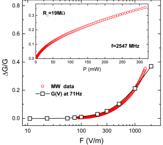
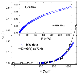
of a given sample is similar but it does not perfectly match the respective (see, for example, figures 3 and 4). There were always some degree of imprecise registry between these functions in all the samples we tested. Such deviations ought perhaps to have been expected. The assumption, implicit to our matching procedure, that it is only the amplitude of the field that matters, is inaccurate; the Miller-Abrahams 12 resistors comprising the hopping system are not purely resistive, and therefore, the local potential drops across the sample may be different at different frequencies.
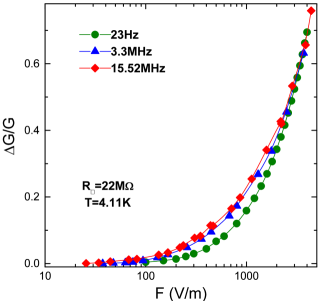
To elucidate this point, we measured at different frequencies on several samples. () was the modulating field applied at frequency while the conductance was monitored at some low-frequency (typically, 20-75 Hz) as in the MW experiments. Here however, we employed frequencies in the 106-108 Hz range so the voltages induced across the sample could be readily displayed and measured by an oscilloscope. Figure 5 shows results of such an experiment. The 3.3 MHz and 15.52 MHz curves in the figure were adjusted to coincide with the 23 Hz plot at =0.7 by re-scaling their voltage axis by a constant, just as in the MW case. This illustrates that the is also a function of the field frequency. Interestingly, above a certain frequency the constant used for re-scaling the curves was somewhat smaller as became higher. Apparently, to achieve the same , larger amplitude is needed at higher . This issue is currently under investigation.
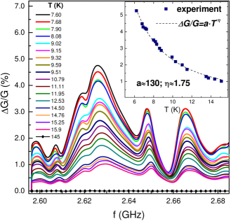
The conjecture that the MW-enhanced conductance is a field-induced non-Ohmic effect is also supported by the temperature dependence of the excess conductance (at constant MW power). In these experiments, was measured over a range of frequencies at each temperature. This was done to cater for drifts in the cavity characteristics with the concomitant shift in conductance-response peaks (see figure 6). The actual drift observed in the figure is remarkably small; note that the series of plots were collected over 3 days because at each temperature the sample was allowed to equilibrate for several hours (the sample is an electron-glass with slow relaxation times 13 ).
The inset to the figure shows due to the MW radiation normalized by at zero field. These experimental points fit reasonably well a power-law which may actually be in qualitative agreement with theory: According to Pollak and Riess 4 , and Shklovskii 3 , at fields just above the ”Ohmic regime” the conductance versus field is given by:
| (2) |
and therefore:
| (3) |
For small this yields:
| (4) |
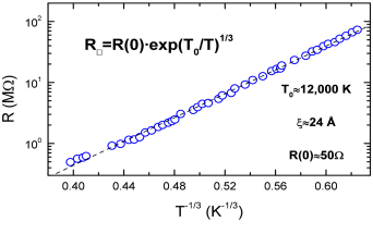
Pollak and Riess associate with the hopping length 4 while Shklovskii associates it with the percolation radius 3 . In either case one expects a power law dependence as indeed observed (see, inset to figure 6). To push the analysis a little further, note that the resistance versus temperature of this sample exhibits Mott’s variable-range-hopping 14 of a two-dimensional system (figure 7). In this case the hopping length scales with temperature as and the percolation-radius scales like giving and respectively. The fit to the data in the inset to figure 6 yields which may suggest that is the relevant length.
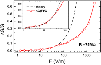
The consistency with theory, as to temperature dependence, encouraged us to test the agreement of the theory 3 with the experiment in a more detailed way. Using the relevant parameters from the data of the sample (figure 7), we estimate the percolation-radius, 5000 Å at 4K ( is the localization-length). This value of is used in equation 2a to plot and the result is compared with the experimentally measured values in figure 8.
This comparison brings to light several problems that need be addressed. The theory may fit the experiment for very small , however, it systematically deviates from the experimental curve when 6 %. This discrepancy is not due to the uncertainty in the value of : The experimental curve is simply not exponential over the range where the effect is more than few percents, (which makes the use of this function questionable). Nor is the range of the studied fields out of the ‘intermediate’ regime. The field where the problem appears is still much smaller than the high-field regime, where the conductance becomes temperature independent 5 ; 15 . On the other hand, if we accept that the fit from 1 V/m to 80 V/m (see inset to figure 8) is in agreement with theory, we have a problem accounting for the condition for the onset of the exponential dependence: This is expected to be given by equation 1, and inserting 1 V/m gives 400m. It is difficult to assign a physical meaning to such a length-scale in a hopping system at 4K.
This problem is commonly encountered in hopping conductivity. Usually, the puzzle is presented in terms of length-scale (being the one parameter in equation 1 that is not ”measured”). Values of this length that are larger by 1-3 orders of magnitude than reasonably expected are reported, or could be inferred, from data in the literature 16 ; 17 ; 18 . These include results for Ge samples doped by nuclear-transmutation 17 , presumed to be relatively free of technical inhomogeneities. Remarkably, the field where non-Ohmicity was already evident in these experiments was smaller by at least 17 a factor of 25 than the theoretical value. These authors 17 find agreement with the Shklovskii model 3 in terms of the temperature dependence of , however, their data fit equation 2 only over a very small range (6 %).
It has been remarked by several authors 16 ; 15 that the origin of the discrepancy between theory and experiment as to the onset-field for non-Ohmicity may be a result of non-uniform field distribution. This might make the field effectively larger than the field one uses in equation 1 based on the measured potential difference across the sample divided by its length. Spatial inhomogeneity is inherent to Anderson insulators, and at least partially, this is actually embodied in the theory in that the system is self-averaging only on scales larger than , which may be quite large at low temperatures. The observation that there has to be a larger length scale to account for the experimental results on different systems suggests that there is an inherent reason not taken into account in the standard hopping models (in addition to imperfections due to technological reasons). There seems to be evidence, based on studies of the onset of non-Ohmic behavior as function of sample-size 19 , that long-range potential-fluctuations may play a role in this phenomenon.
Note, incidentally, that the sub-linearity of at small fields follow naturally from theoretical models that predict 1 ; 3 ; 4 . The Apsley and Hughes model 2 that expects yields a linear dependence at small however, it does not fit the measured any better than the other models. It is unfortunate that neither model may be trusted to fit experiments on real systems except over a limited range of fields. Given this situation, comparing the MW-enhanced conductance with the experimentally measured is the only option one has for a meaningful test.
The similarity between the field assisted and the MW-enhanced conductance and the qualitative agreement with theory make a strong case for the mechanism we propose. This is a plausible scenario for the MW frequency regime employed in this study as the associated wavelength is larger than the sample size.
IV Acknowledgments
This work greatly benefited from the insightful remarks by M. Pollak and from the many helpful discussions with B. Shapiro during the Electron-Glasses program held at Santa-Barbara. The author expresses gratitude for the hospitality and support of the KAVLI institute that hosted this program. Illuminating discussions with A. Frydman and A. Goldman at the later stage of this work are gratefully acknowledged. Thanks are also due to X. M. Xiong, and P. W. Adams for the Be samples, and to N.V. Agrinskaya for the GaAs sample. This research was supported by a grant administered by the US Israel Binational Science Foundation and by the Israeli Foundation for Sciences and Humanities.
References
- (1) R. M. Hill, Philos. Mag. 24, 1307 (1971).
- (2) N. Apsley and H. P. Hughes, Philos. Mag. 31, 1327 (1975).
- (3) B. I. Shklovskii, Fiz. Tekh. Poluprovodn. 6, 2335 (1972) [Sov.Phys. Semicond. 6, 1964 (1973)].
- (4) M. Pollak and I. Riess, J. Phys. C9, 2339 (1976).
- (5) B. I. Shklovskii, Fiz. Tekh. Poluprovodn. 10, 1440 (1976) [Sov.Phys. Semicond. 10, 855 (1976)].
- (6) I. P. Zvyagin, phys. stat. sol. (b) 88, 149 (1978).
- (7) M. Ben-Chorin, Z. Ovadyahu and M. Pollak, Phys. Rev. B 48, 15025 (1993).
- (8) Z. Ovadyahu, Phys. Rev. Lett., 102, 206601 (2009).
- (9) A. Vaknin, Z. Ovadyahu, and M. Pollak, Phys. Rev. B 65, 134208 (2002).
- (10) Z. Ovadyahu, Phys. Rev. B 78, 195120 (2008).
- (11) The MW-induced voltage across the sample (with 10 s) could not have been measured in this work.
- (12) A. Miller and E. Abrahams, Phys. Rev. 120, 745 (1970).
- (13) A. Vaknin, Z. Ovadyahu, and M. Pollak, Phys. Rev. Lett., 81, 669 (1998).
- (14) N. F. Mott and E. A. Davis, in: ”Electronic Processes in Non-Crystalline Materials”, Clarendon Press, Oxford (1979).
- (15) O. Faran and Z. Ovadyahu, Solid State Commun., 67, 823 (1988); D. Shahar and Z. Ovadyahu, Phys. Rev. Lett. 64, 2293 (1990).
- (16) T. F. Rosenbaum, K. Andres, and G. A. Thomas, Solid State Commun., 35, 663 (1980).
- (17) Ning Wang, F. C. Wellstood, B. Sadoulet, E. E. Haller, and J. Beeman, Phys. Rev. B 41, 3761 (1990).
- (18) C. Godeta; Sushil Kumara; V. Chub, Philos. Mag. 83, 3351 (2003).
- (19) D. Kowal and Z. Ovadyhau, Physica C, 468, 322 (2008).