A giant red shift and enhancement of the light confinement in a planar array of dielectric bars
Abstract
The results of the research of resonant phenomena in double-periodic subwavelength planar structures made up of paired dielectric bars are presented. For the first time the existence of high Q-factor trapped mode resonances is revealed in these low-loss entirely dielectric structures. A great red shift of the trapped mode resonance of the structure is observed as compared with the resonant wavelength of the periodic structure with only one dielectric bar per unit cell. This shift of the resonant wavelength is caused by a strong coupling of the electromagnetic fields in the adjacent dielectric-bar resonators.
pacs:
42.25.Fx, 42.25.Gy, 42.70.Qs, 42.79.Dj, 78.67.-nKeywords: Trapped mode, Fano resonance, planar dielectric array, germanium periodic structure, light diffraction, infrared wave diffraction.
1 Introduction
Thanks to a striking progress in nanotechnology, the optically thin layers of materials can be structured with periodic pattern in order to design planar metamaterials. The planar metamaterials (also known as metafilms) are an impressive modern object, which is driven by certain fascinating facilities such as, e.g., the anomalous reflection and refraction [1], the unusual asymmetric transmission [2, 3], and light reflection that does not change the phase of the incident wave [4].
Typically, a planar metamaterial assigned for visible and near infrared wavelengths is a plasmonic structure designed on the basis of a periodic array of complex-shaped resonant nanowire metallic particles. The main factor responsible for the spectacular properties of metafilms is some resonant interaction of light with the patterned layer. Moreover, numerous envisioned applications of planar metamaterials do require the high Q-factor resonances and a strong confinement of intensive electromagnetic fields. First of all they concern both the projects of gaining or lasing devices such as the spaser [5, 6] and the devices characterized by the bistable reflection and transmission in order to control light with light [7, 8], which could be realized by incorporating some active medium or nonlinear inclusions in periodic structures of resonant metafilms. Another domain, aging a decade, concerns the extremely sensitive chemical and biochemical sensors [9].
However, losses are orders of magnitude too large for the envisioned applications. Typically, the Q-factor of the resonances excited in plasmonic structures is small because of high radiation losses and huge energy dissipation inherent to metals in the visible and near infrared wavelength ranges.
The usual resonance field enhancement inside a planar metamaterial may be extremely increased by involving structures which bear the so-called trapped modes [10, 11]. The excitation of the trapped mode resonances in planar double-periodic structures with broken symmetry was found both theoretically [12, 13, 14] and experimentally [15] in microwaves. In particular, those typical peak-and-trough Fano spectral profile resonances can be excited in the periodic array composed of twice asymmetrically-split metal rings. Their specific character arises from some destructive interference of the radiation by the anti-phased currents in metallic elements of a subwavelength periodic cell.
In the fully symmetric structure, the coupling of the trapped mode currents can be infinitesimal for a wave incident from free space. Thus, the Q-factor of the resonance is limited only by the dissipative losses of the structure. This unique property leads to the analogy between the trapped mode resonance and the metastable energy level in atomic systems, manifesting an electromagnetically induced transparency. Recently, some effective media exhibiting the EIT-like properties and the desired ”light slowing” metamaterials that use the trapped mode plasmonic arrays, have been proposed [16, 17].
Now, the existence conditions and the spectral properties of trapped mode resonances are investigated in detail in the suitably structured planar plasmonic metamaterials developed for the near-IR range [18, 19, 20]. The Q-factor of the trapped mode resonance essentially exceeds that for the ordinary resonance, but its value is not greater than several tens because of dissipative losses.
Since the intrinsic dissipative losses in plasmonic structures are unavoidable, the idea of their compensation using certain parametric processes and gain media was proposed [21, 22]. Experimental demonstrations of the compensation of the absorption losses in a trapped-mode metallic metamaterial by using optically pumped semiconductor quantum dots were presented in [23, 24]. The observed narrowing of the quantum dots photoluminescence spectrum evidences of the Q-factor increase in the pumped structure.
Fortunately, the use of plasmonic structures is not a single possible way to develop the thin planar metamaterials to ensure a strong enhancement of the confined resonant field. One evident way to produce low-dissipative structures, with similar electromagnetic properties is to use entirely dielectric elements in designing the double-periodic structures maintaining the trapped mode resonances. It was shown recently, by simulation, that the microwave left-handed media may be constructed on the basis of cubic high dielectric resonators [25] or dielectric rings and rods put together [26] instead of the classical split-ring metallic resonators.
This paper is aimed at involving in the family of the high-Q trapped mode planar metamaterials the new and highly desirable low-loss structures made up of entirely dielectric elements.
The resonances in the plasmonic and dielectric structures have a considerably different nature. A plasmon-polariton excitation propagating along metallic surfaces replicates their shape. Therefore, the complex-shaped metallic elements can be used to provide a resonant interaction light with a periodic structure in a deeply subwavelength range. On the contrary, complications of the shape of dielectric elements do not involve a substantial increase of the resonant wavelength, like in the case of metallic elements.
The paper studies the excitation conditions and the main properties of the near-infrared trapped-mode resonance in a low-loss subwavelength planar array with the unit cell that includes a pair of resonant dielectric bars.
2 The problem statement and the method of solution
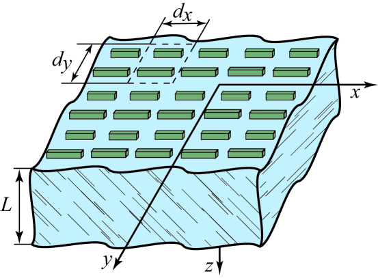
Let us consider a dielectric bar of square cross section as a constituent element of the entirely dielectric array. Thus the problem of light diffraction by a double-periodic planar array of dielectric bars placed on a substrate with thickness is under investigation (see Fig. 1). The unit cell of the array includes a pair of dielectric bars which have different in length but identical in cross-section and material. The longer bar length is and the shorter . The sizes of the square periodic cell are nm. The distance between the longer and the shorter bars of the pair is 195 nm for all of the two-element dielectric arrays studied below. The periodic cell is symmetric relative the line drawn through the cell center parallel to the -axis. The normal incidence of a linearly -polarized plane wave is considered. The resonant response of the array is studied in the near infrared wavelength range from 1000 nm to 3000 nm. The substrate material is assumed to be synthetic fused silica. Its refractive index is approximately 1.44 in the wavelength range under consideration [27].
In order to provide a resonant light reflection without forming the diffraction orders, the dielectric bars are chosen to have the resonant wavelength larger then the unit cell size. The size of the dielectric bar cross-section is restricted by the following condition where is the bar relative permittivity and is the cross section size; this eliminates the transverse interference resonances inside bars.
The bar permittivity value is substantially limited by the properties of dielectric materials suitable for the dielectric array manufacture. The usual dielectrics extensively used in microchip technologies have permittivities not exceeding 4. However, some semiconductors can be used as materials for the array elements. The use of semiconductors is promising because they have the transparency windows in the visible and near-infrared wavelength ranges. The permittivity of well-known suitable semiconductors has a value from 11 to 18 and their dielectric loss tangent does not exceed within the transparency windows. For example, the germanium transparency window extends from 1600 nm to 2000 nm and its refractive index varies from 4.07 to 4.23 over this window [28].
Taking into account everything mentioned above, the size of the square cross section of dielectric bars is chosen to be nm.
To solve the diffraction problem, the numerical method proposed in [29] is used. This method is based on both the mapped PSTD method [30] and the transfer matrix theory. For the simplicity the dispersion of dielectrics is not taken into account in this paper. The relevancy of such approach is due to two reasons. First, the dispersion of the chosen materials is very weak in the wavelength range considered. Next this, dispersion has no effect on the properties of the trapped-mode resonances. However, the constituents dispersion may be taken into account in the context of the method used.
3 The trapped mode resonances in the arrays of dielectric bars
Let us assume that silica fills up the all the half space below the array to simplify the analysis by excluding the interference resonances in the substrate. As known, and shown by simulation in [29], the finite thickness of the substrate results in the interference fringes along the wavelength dependences of the reflection and transmission coefficients. In the actual structures approximately 0.5 mm thick, these interference resonances are destroyed because of local inhomogeneity of the substrate.
3.1 The resonant properties of the arrays composed of metallic bars
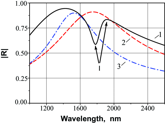
For further comparison between the resonant properties of plasmonic and entirely dielectric planar metamaterials, and to begin with, let’s briefly mention the reflection wavelength dependences of the arrays of gold bars. The square unit cell of the structure considered has nm. The longer and shorter bar lengths are 450 nm and 400 nm respectively. The minimal distance between the longer and the shorter bars is 100 nm. The array is placed on the silica semi-infinite substrate. Since metals have a strong inherent dispersion in the near infrared range, the gold dispersion has been taken into account by using the complex-pole model and the method of additional differential equation (see, for example [20]).
The wavelength dependence of the reflection coefficient magnitude of this structure is shown in Fig. 2 (line 1). Another two lines present the wavelength dependences of the reflection coefficient magnitudes of the arrays with a single gold bar in the periodic cell. The line 2 corresponds to the array which consists of the longer bars from the two-element array and the line 3 to the array of the shorter ones.
The trapped mode resonance is marked by I in Fig. 2. It has the typical trough-and-peak Fano spectral profile [31]. As is well known [20, 19], this resonance results from the excitation of the anti-phased plasmon-polaritons in the adjacent metallic bars. One important point is that the trapped mode resonance of the two-element periodic structure is excited in the wavelength band restricted by the wavelengths of the reflection resonances of the one-element arrays or in a wavelength close to this band. It is easily seen from the spectral dependences in Fig. 2 and presented in [19].
3.2 Identification of the reflection resonances of a subwavelength dielectric array
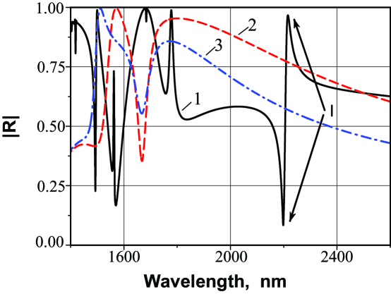
First of all, in order to identify the kind of resonances, is considered the normal reflection by arrays which are assumed to be made of a hypothetic lossless dielectric with the large refractive index 5.5. Such special choice of the refractive index enables to observe at least two reflection resonances of one-element arrays of dielectric bars in the subwavelength range. The wavelength dependences of the reflection coefficients magnitudes are shown in Fig. 3 for both the array of paired dielectric bars (line 1) and the one-element arrays. The lines 2 and 3 correspond to the array of the longer and the shorter dielectric bars, respectively. There are two reflection resonances of the one-element arrays in the considered wavelength range. As revealed by the numerical analysis of the electric field distributions along the periodic cell of arrays, they are the ordinary resonances of dielectric bars. These resonances are excited under the condition that the bar length is approximately equal to or where is the wavelength in the dielectric of bars.
If two bars of different length are combined in the periodic cell, some additional reflection resonances are excited (see Fig. 3, line 1). Especial interest is stimulated by the additional resonance in the long-wave part of the considered range. It is a typical Fano-shape sharp resonance with a specific wavelength dependence of the reflection coefficient rolled over deep to peak.
The electric field distributions within the periodic cell have been plotted and studied over for all of the additional resonances, to clarify their nature. One of such distributions relating to the plane is shown in Fig. 4 at the wavelength 2208 nm that corresponds to the additional resonance with the maximum wavelength. As the field has a symmetric distribution, it is presented only within a half of the cell.
One can see that the both dielectric bars behave as a half-wavelength dielectric resonators, i.e. the maximum of the electric field within the bar locates close to its center and the field decreases to the bar facets (Fig. 4,b). The electric field maxima observed outside the bar at its ends result from large enough difference between the permittivities inside and outside the bar. Actually, the normal components of the electric field induction satisfy the continuity condition , where and are the electric fields in free space and inside the bar, respectively. Thus the electric field in free space between the bars has the value times grater than the field inside the bars. In our case this coefficient is . The antiphased field distribution evidences that the studied resonance is a trapped mode one. Notice that the field component has its maximum value of the same order as the maximum of the and the maximum of one is over then 100 times less.
Besides the enhanced Q-factor, the main distinctive feature of the trapped-mode resonance of the two-element dielectric array is a great red shift of its wavelength relative the resonant wavelengths of the corresponding one-element arrays (see Fig. 3). Thus the coupling between the dielectric bars of the two-element periodic array results in an extremely large increase of the resonant wavelength as opposed to the coupling in the array of metallic bars (see Fig. 2). This property of the entirely dielectric trapped-mode arrays is quite important in view of possible applications in the field of infrared metamaterials. First, the ratio of the array pitch to wavelength may be decreased to design more homogeneous metamaterials. Second, the increase of the resonant wavelength results in an enhancement of the confinement of the field intensity due to a decrease of radiation losses. It is equally important to designing of nonlinear and active artificial media. Third, this property of dielectric arrays gives us a way to design double-periodic structures with the trapped mode resonance using materials of relatively small refractive index; for example, made of semiconductors in the wavelength range of their transparency windows.
Finally, the research of the field distributions concerning all the rest resonances of the studied over two-element dielectric array (see the spectral dependence in Fig. 3, line 1) results in the conclusion that they are the ordinary dimensional resonances.
3.3 The trapped mode resonance of a germanium-bar array within the transparency window bandwidth
Now let us study some more realistic array of the germanium bars with the sizes mentioned above. The refractive index of germanium is assumed to be equal to 4.12. Such value of the germanium refractive index corresponds to the wavelength range from 1850 to 1950 nm. This range is a shaded one in Fig. 5 where the wavelength dependence of the reflection coefficient of the array is presented. The trapped mode resonance is observed in this range.
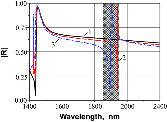
Fig. 5 illustrates the effect of the array asymmetry as a consequence of the influence of the difference of bar lengths on the wavelength and the Q-factor of the trapped mode resonance. It is evident that the trapped mode resonance cannot be excited in a symmetrical structure with equal lengths of both bars by the normally incident plane wave because of the zeroth coupling of asymmetrical mode of bars and plane wave in the free space and substrate (see line 1 in Fig. 5). A decrease of the asymmetry degree characterized by the value results in an increase of the red shift of the trapped mode resonance and a decrease of the wavelength difference between the reflection deep and peak, i.e. in the trapped mode resonance Q-factor growth.
To estimate the trapped mode resonance Q-factor consider the expression , where and are the wavelengths of the deep and peak of the reflection coefficient, respectively, and is the wavelength corresponding to the reflection coefficient value . The Q-factors of the trapped mode resonances of the germanium bars structures are 203 and 1080 for nm, nm and nm, nm, respectively (see the lines 2 and 3 in Fig. 5 for comparison). Note that for the structure of the dielectric bars with the refractive index 5.5 (see Fig. 3, line 1), the Q-factor of the trapped mode resonance is 127.
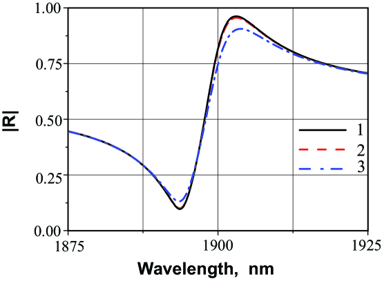
The semiconductors dissipative losses will certainly effect the Q-factor of the trapped mode resonance. However, in the transparency window the dielectric loss tangent of germanium does not exceed (this bandwidth is marked as shaded in Fig. 5). Over this band, one can see only negligible variations of the reflection magnitude and a very small widening of the trapped mode resonance which reveals a decrease of the Q-factor (see Fig. 6) with an increase of the dielectric loss tangent.
The field of high intensity confined in the periodic array under the trapped mode resonance may effectively interact with a substrate of an active or nonlinear material. In the first case, one can observe amplification of the reflected or the transmitted light. In the case of a nonlinear substrate, a certain light with light controlling can be achieved in very thin structures.
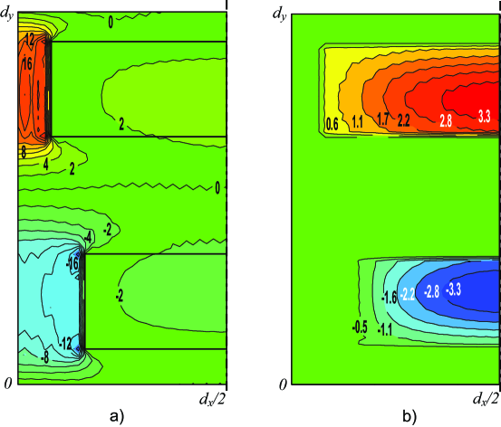
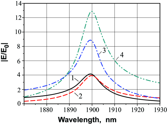
The wavelength dependences of the ratio are presented in Fig. 7. Here is the maximum of the absolute value of the electric field in one or another chosen point within the array and is the maximum of the absolute value of the incident wave electric field in free space. The wavelength dependences of are shown for four different points. Lines 1 and 2 correspond to the centers of the shorter and the longer dielectric bars, respectively. Near those points the electric field reaches its maximum level inside the bars. Lines 3 and 4 correspond to the center of a gap between two adjacent shorter and longer bars, respectively. It should be noticed that the electric field magnitude reaches its minima along the both mentioned gaps in these points (see Fig. 4,a). The magnitude of electric field enlarges over 28 times in the center of the gap between the bars despite the fact that the electric field has its minimum in these points. The maximum of the electric field magnitude in array corresponds to the wavelength 1899 nm. This wavelength is approximately equal to the central wavelength of the trapped mode resonance ( nm).
The Q-factor increasing results in a rise of the electric field intensity in the structure. For example, the maximal ratio is 2.3 times greater in the case of the germanium array with nm and nm than with the array with nm and nm.
4 Conclusions
The problem of the normal reflection of the near-infrared radiation by a planar array with a subwavelength square translation cell composed of two dielectric bars of different lengths has been solved. For the fist time the existence of the high-Q trapped-mode resonance has been found out in these low-loss entirely dielectric structures. A coupling between the adjacent bars induces the field enhancement in the surrounding media; which can enforce the phenomena like luminescence, nonlinear scattering, absorption, and lasing. The spectral response of this novel planar metamaterial closely resembles the EIT phenomenon in atomic systems. In contrast with plasmonic arrays, the trapped-mode resonance excited in an entirely dielectric structure demonstrates a giant red shift relative to the wavelength of the ordinary resonance of array with only one dielectric bar per unit cell. This remarkable property of the dielectric trapped-mode arrays enables to design the highly desirable deep-subwavelength low-loss planar metamaterials in near infrared range.
References
References
- [1] Yu N, Genevet P, Kats MA, Aieta F, Tetienne JP, Capasso F, et al. Light propagation with phase discontinuities: generalized laws of reflection and refraction. Science 2011;344:333–337.
- [2] Fedotov VA, Mladyonov PL, Prosvirnin SL, Rogacheva AV, Chen Y, Zheludev NI. Asymmetric propagation of electromagnetic waves through a planar chiral structure. Phys Rev Lett 2006;97(16):167401(4).
- [3] Fedotov VA, Schwanecke AS, Zheludev NI, Khardikov VV, Prosvirnin SL. Asymmetric transmission of light and enantiomerically sensitive plasmon resonance in planar chiral nanostructures. Nano Letters 2007;7(7):1996–1999.
- [4] Schwanecke AS, Fedotov VA, Khardikov VV, Prosvirnin SL, Chen Y, Zheludev NI. Optical magnetic mirrors. J Opt A: Pure Appl Opt 2007;9(1):L1–L2.
- [5] Bergman DJ, Stockman MI. Surface plasmon amplification by stimulated emission of radiation: Quantum generation of coherent surface plasmons in nanosystems. Phys Rev Lett 2003;90(2):027402.
- [6] Zheludev NI, Prosvirnin SL, Papasimakis N, Fedotov VA. Lasing spaser. Nature Photonics 2008;2(6):351–354.
- [7] Tuz VR, Prosvirnin SL, Kochetova LA. Optical bistability involving planar metamaterials with broken structural symmetry. Phys Rev B 2010;82:233402(4).
- [8] Carretero-Palacios S, Minovich A, Neshev DN, Kivshar YS, Garcia-Vidal FJ, Martin-Moreno L, et al. Optical switching in metal-slit arrays on nonlinear dielectric substrates. Opt Lett 2010;35(24):4211–4213.
- [9] Flory F, Escoubas L, Berginc G. Optical properties of nanostructured materials: a review. Journal of Nanophotonics 2011;5:052502(1–20).
- [10] Stockman MI, Faleev SV, Bergman DJ. Localization versus delocalization of surface plasmons in nanosystems: Can one state have both characteristics? Phys Rev Lett 2001;87(16):167401–4.
- [11] Liu HC, Yariv A. Grating induced transparency (git) and the dark mode in optical waveguides. Optics Express 2009;17(14):11710–11718.
- [12] Prosvirnin SL, Zouhdi S. Multi-layered arrays of conducting strips: Switchable photonic band gap structures. Int J Electron Commun (AEÜ) 2001;55(4):260–265.
- [13] Prosvirnin S, Zouhdi S. Resonances of closed modes in thin arrays of complex particles. In: Zouhdi S, et al, editors. Advances in Electromagnetics of Complex Media and Metamaterials. Printed in the Netherlands: Kluwer Academic Publishers; 2003. p. 281–290.
- [14] Blackburn JF, Arnaut LR. High performance split ring fss for wlan bands. In: Proc. 27th ESA Antenna Technology Workshop on Innovative Periodic Antennas: Electromagnetic Bandgap, Left-handed Material, Fractal and Frequency Selective Surfaces. Santiago de Compostela, Spain: European Space Agency; 2004. p. 329–336.
- [15] Fedotov VA, Rose M, Prosvirnin SL, Papasimakis N, Zheludev NI. Sharp trapped-mode resonances in planar metamaterials with a broken structural symmetry. Phys Rev Lett 2007;99(14):147401.
- [16] Zhang S, Genov DA, Wang Y, Liu M, Zhang X. Plasmon-induced transparency in metamaterials. Phys Rev Lett 2008;101(4):047401(4).
- [17] Papasimakis N, Fedotov VA, Zheludev NI, Prosvirnin SL. Metamaterial analog of electromagnetically induced transparency. Phys Rev Lett 2008;101(25):253903(4).
- [18] Khardikov VV, Iarko EO, Prosvirnin SL. Trapped-mode resonances in light diffraction by a planar doubly periodic structure with asymmetric metal elements. Radio Physics and Radio Astronomy 2010;1(3):221–231.
- [19] Dong ZG, Liu H, Xu MX, Li T, Wang SM, Zhu SN, et al. Plasmonically induced transparent magnetic resonance in a metallic metamaterial composed of asymmetric double bars. Opt Express 2010;18(17):18229–18234.
- [20] Khardikov VV, Iarko EO, Prosvirnin SL. Trapping of light by metal arrays. J Opt 2010;(12):045102(11).
- [21] Popov AK, Shalaev VM. Compensating losses in negative-index metamaterials by optical parametric amplification. Opt Lett 2006;31(14):2169–2171.
- [22] Gordon JA, Ziolkowski RW. The design and simulated performance of a coated nano-particle laser. Optics Express 2007;15(5):2622–2653.
- [23] Plum E, Fedotov VA, Kuo P, Tsai DP, Zheludev NI. Towards the lasing spaser: controlling metamaterial optical response with semiconductor quantum dots. Opt Express 2009;17(10):8548–8551.
- [24] Tanaka K, Plum E, Ou JY, Uchino T, Zheludev NI. Multifold enhancement of quantum dot luminescence in plasmonic metamaterials. Phys Rev Lett 2010;105:227403(4).
- [25] Kim J, Gopinath A. Simulation of a metamaterial containing cubic high dielectric resonators. Phys Rev B 2007;76(11):115126(6).
- [26] Jelinek L, Marqu’es R. Artificial magnetism and left-handed media from dielectric rings and rods. J Phys: Condens Matter 2010;22:025902(6).
- [27] Malitson IH. Interspecimen comparison of the refractive index of fused silica. JOSA 1965;55(11):1205–1208.
- [28] http://www.filmetrics.com:80/refractive-index-database/ge/germanium;.
- [29] Khardikov VV, Iarko EO, Prosvirnin SL. Using transmission matrix and pseudospectral time-domain method to study of light diffraction on planar periodic structures. Radiophysics and Radioastronomy 2008;13(2):146–158.
- [30] Gao Xian, Mirotznik MS, Shi S, Prather DW. Applying a mapped pseudospectral time-domain method in simulating diffractive optical elements. J Opt Soc Am A 2004;21(5):777.
- [31] Fano U. Effects of configuration interaction on intensities and phase shifts. Phys Rev 1961;124(6):1866–1878.