Vibrationally induced flip motion of a hydroxyl dimer on Cu(110)
Abstract
Recent low-temperature scanning-tunneling microscopy experiments [T. Kumagai et al., Phys. Rev. B 79, 035423 (2009)] observed the vibrationally induced flip motion of a hydroxyl dimer (OD)2 on Cu(110). We propose a model to describe two-level fluctuations and current-voltage characteristics of nanoscale systems which undergo vibrationally induced switching. The parameters of the model are based on comprehensive density-functional calculations of the system’s vibrational properties. For the dimer (OD)2 the calculated population of the high and low conductance states, the , , and curves are in good agreement with the experimental results and underlines the different roles played by the free and shared OD stretch modes of the dimer.
Electron transport through single-molecule junctions has been receiving enthusiastic interest for a development of novel molecular devices. Nonlinear characteristics associated with the vibrationally mediated configurational change with different conductances have been observed in a series of systems such as pyrrolidine on a Cu(001) Gaudioso , H2 on Cu Gupta , CO bridging a Pt contact Thijssen , and H2 in Au contactsAuH2 . In these systems spectra show anomalous spikes—in contrast to steps usually observed in inelastic electron tunneling spectroscopy (IETS)Stipe_Science —at the bias voltage related to the vibrational mode energies.
Recently Kumagai et al.Kumagai_2009 studied the dynamics of a single hydroxyl (OH, OD) molecule and the dimer (OD)2 on Cu(110) using a scanning tunneling microscope (STM). The STM images observed for the monomer suggested the possible quantum tunneling of a hydroxyl between two equivalent adsorption configurations on Cu(110), as supported by the density functional theory (DFT) calculations of the transition path and rate of the flipping of OH on Cu(110) Davidson . This spontaneous flip motion of hydrogen atoms in the monomer is quenched for the dimer at low temperatures, but can be induced by excitation of the OH/OD stretch mode by tunneling electrons. Time-averaged measurements of the current show a non-linear current () increase at the bias voltage () inducing the transition from the high and low conductance states. The appearance of the peak in and the peak and dip in from transitions between states with distinct conductances have also been reported previously Gupta ; Thijssen ; AuH2 .
In this paper a combined use of the DFT-based SIESTA SIESTA , TranSIESTA TRANSIESTA and Inelastica INELASTICA ; INELASTICA2 packages permits us to gain insight into the elementary processes that induce the flip motion of the asymmetric dimer. The extensive DFT calculations provide the ground state geometry, vibrational modes, electron-vibration couplings, emission rate of vibrations from tunneling electrons, vibrational damping due to electron-hole pair excitation, and the high and low conductance. These calculated properties allow us to model the population of the high and low conductance states as a function of the bias voltage and the nonlinear characteristics for (OD)2 on a Cu(110) surface. The experimental results (relative occupation of the high and low conductance state, curve, and ) are nicely reproduced, and the different roles played by the free and shared OD stretch modes in the vibrationally mediated configurational flip motion are clarified.
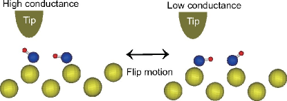
The telegraph switching between high- and low-conductance states of (OD)2 is shown schematically in Fig. 1. In low-temperature STM, no spontaneous switching is observed at low bias since the barrier for the reaction is substantialKumagai_2009 . Keeping the STM tip stationary and increasing bias over approximately 200 meV the switching between the two degenerate low-energy configurations is triggered by phonon emission. However, the reaction rate remains rather small until the bias exceeds the (OD) stretch vibrations ( 300-330 meV). We denote the two configurations as the high () and low () conductance states where the tip-dimer distance is smaller for the configuration.
To investigate the flip motion of the dimer (OD)2 we performed calculations on a 6 atom thick Cu slab using periodic boundary conditions. The tip was modeled as one protruding Cu atom on the reverse side of the slab. All calculations were performed with the PBE GGA functional, DZP (SZP) basis set for dimer (bulk Cu), -point sampling, and a 300 Ry mesh cutoff. The elastic transport properties were calculated using the DFT+NEGF method where 6 additional layers of Cu were used to connect the central region to semi-infinite metallic leads. Fig. 1 shows the schematic side view of the dimer in the and conductance states. The calculated low-bias conductance ratio closely matches the experimental ratio. However, the calculated absolute conductances are much larger than in the experiment since numerical considerations demand the calculations to be performed at a small tip-dimer distance. The relaxed hydrogen-bonded OD-O distance is 2.90 Å while the OD bond length and tilt angle to the surface normal are 1.00 (0.98) Å and 81∘ (51∘), respectively. The two hydroxyl groups, bonded near adjacent bridge sites along (001) are oriented according to the optimal configuration for hydrogen bonding. The D atom pointing towards the adjacent OD molecule form the OD-O bond (with characteristic shared OD stretch mode) in contrast to the D atom pointing away from the adjacent OD molecule (with free OD stretch mode). These nonequivalent configurations of each OD molecule lift the degeneracies of the vibrational energies for the two OD molecules.
The vibrational modes and frequencies of the molecular adsorbates and the corresponding electron-phonon couplings are calculated from a finite difference schemeINELASTICA ; INELASTICA2 . These calculations were repeated with the tip scanned over the surface as indicated by the black dots in Fig. 2. Table I lists the calculated vibrational modes for the and configurations. Here (OD) labels the free OD stretch mode, (OD-O) the shared OD stretch mode involving the D atom between two oxygen atoms, and rotxy(z) rotation modes in the surface plane (surface normal). Values for the low-energy modes mainly involving motion of the oxygen atoms have been omitted from the table.
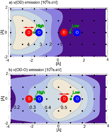
In addition to the vibrational energies (), the electron-hole pair damping rate and vibration generation rate were calculated for each tip position within the lowest order expansion (LOE) schemeINELASTICA ; INELASTICA2 . In the low-temperature limit the emission rate is give by
| (1) |
where is the applied bias, the step function, and the emission rate constant written in terms of electron-phonon coupling matrix and partial spectral density at the Fermi energy, cf. Ref. INELASTICA, . The spectral density can further be rewritten in terms of a sum over scattering states at the Fermi-energy incident from substrate / tip (1/2) showing the equivalence of the LOE scheme with the Fermi-golden rule, assuming a constant density of states around the Fermi-energy.INELASTICA Furthermore, for weak coupling between tip-adsorbate, the emission rate constants scale with the tip-adsorbate coupling () squared (). Since the current scales in the same way, the emission rate at a given voltage is proportional to the current. The electron-hole pair damping rate is insensitive to the position of the STM tip since the damping is dominated by the metal surface. The emission rate map for the two (OD) and (OD-O) modes are shown in Fig. 2 where the emission rates were calculated by scanning the tip over the surface at a constant height of 5.6 Å above the oxygen atoms, i.e., the DFT calculations of e-ph coupling, transmission, emission rates, and damping were repeated for geometries with the tip displaced relative to the OD dimer. We note that the emission rate for the free OD stretch is more localized around the high conductance site than the shared OD-O stretch mode which is also evident from Table I. The green points in Fig. 2 correspond to the and configurations listed in Table 1.
| Mode | |||
|---|---|---|---|
| (OD) | 327.2 | 0.17 | 47.3 |
| (OD) | 326.6 | 4.42 | 52.3 |
| (OD-O) | 301.2 | 0.49 | 248.0 |
| (OD-O) | 301.8 | 0.35 | 249.6 |
| rotz(OD-O) | 76.8 | 1.19 | 250.7 |
| rotz(OD-O) | 76.5 | 0.67 | 268.0 |
| rotxy(OD-O) | 77.0 | 0.24 | 103.7 |
| rotxy(OD-O) | 76.9 | 0.10 | 76.0 |
| rotxy(OD) | 51.8 | 0.01 | 59.4 |
| rotxy(OD) | 52.6 | 0.71 | 60.7 |
| rotz(OD) | 49.9 | 0.27 | 97.0 |
| rotz(OD) | 49.8 | 0.79 | 86.6 |
To describe vibrationally induced switching in nanoscale systems we propose a simple model which expresses the current in terms of the occupation and conductance of the and conductance states,
| (2) |
where is determined as a stationary solution of the rate equations,
| (3) | |||||
| (4) |
with the condition . This gives
| (5) |
where is the transition rate from to . The experiments show that the reaction rate at a constant voltage is propotional to the current, i.e., the reaction rate is proportional to the emission rate of the vibrations. The simplest way to model the transition rates is therefore to assume a linear dependence on the vibrational occupation or equivalently the vibrational generation rates Ueba_Sergei_2010 , i.e.,
| (6) |
where a constant rate is introduced to model the collective effect of many low-energy vibration modes and where represents the broadened vibrational generation rateMotobayashi of a distinct mode given by
| (7) |
In the above equation we use a Gaussian distribution function characterized by a standard deviation . The prefactors describe the likelihood of the generated vibrational excitation to induce the flip motion, i.e., the probability of transferring the motion from the vibration to the reaction coordinateUeba_Sergei_2010 .
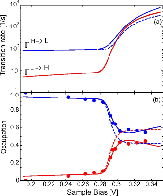
We obtain a good fit to the experimental OD dimer data from Ref. Kumagai_2009, considering only three different vibrational modes, see Fig. 3. The fitting parameters used are (, 327.2/326.6 meV, 20 meV) for (OD), (, 301.2/301.8 meV, 8 meV) for (OD-O), (, meV, 19 meV) for rotz(OD-O), and s-1. We first note that we need to use large values for the broadening meV to fit the experimental data. We believe this to be caused by the statistical nature of the experimental data collection and do not reflect thermal or phonon DOS broadeningMotobayashi . The fitting constants and are only determined up to a multiplicative factor since the occupations are determined by the ratios in Eq. (5). We choose the prefactor of the shared (OD-O) mode as the reference and set it to based on an order of magnitude estimate from the experimental flip frequencyKumagai_2009 . The values for only determine the low-bias occupation where because the system is experimentally only observed in the configuration. The reason for this preference of at low bias might be due to the larger current and thus larger vibrational generation rate of low-energy phonons in the configuration. However, in the intermediate bias range meV we see a slight change in the occupation as shown in Fig. 3(b). Although we cannot unambiguously assign a vibrational mode to this change in occupation from the available experimental data, we have chosen to model this by the rotz(OD-O) mode. In contrast, there is much less latitude in the fitting parameters for the (OD) and (OD-O) modes. We note that the change in occupation at 300 meV do not fit with the free (OD) vibrational energy ( 330 meV) and clearly indicate that the shared (OD-O) mode is the main culprit in inducing the flip motion. This assignment is supported by the fact that the occupation quickly approaches 50/50 which implies that the emission rate constants of the high- and low-conductance states are of similar magnitude. This is clearly not the case for the free (OD) but true for the (OD-O) mode, see Tab. 1 and Fig. 2. To underline the effects of the shared (OD-O) and free (OD) stretch modes Fig. 3 shows the full modeling (solid line) and without the free (OD) vibration (dashed line). Without the (OD) mode, the occupation rapidly approach the ratio of the shared (OD-O) emission rate constants . Note that the approximately equal occupation of the / states is a coincidence and that the ratio of the occupations at high bias is simply given by the ratio of emission rate constants and the fitting constants . In contrast to the shared (OD-O) mode, which increases the state occupation, the main effect of the free (OD) mode is a slight increase of the transition rate, Fig. 3(a), and thereby slightly decreases the occupation of the state.
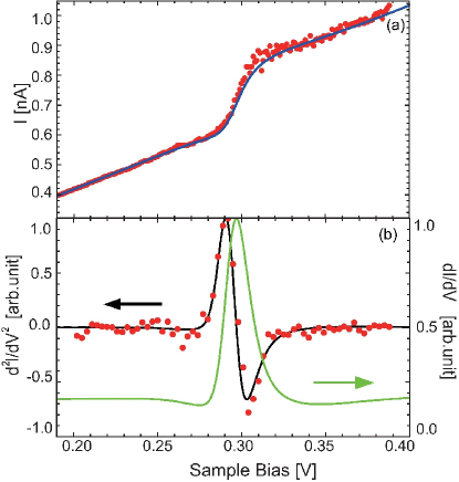
Using the calculated conductances ( nA/V, nA/V) scaled by the constant factor to account for the small tip-sample distance used in the calculation and the bias dependent population [, ] shown in Fig. 3(b), the characteristics were calculated from Eq. (2). As shown in Fig. 4 the calculated time averaged curve [Fig. 4(a)] and [Fig. 4(b)] show remarkable agreement with the experimental results. We note that the lineshape of the signal is clearly different from inelastic electron tunneling spectra which normally only shows a peak or dipPaulsson2005 . In addition, the size of the signal from the vibration is much larger than what one normally associates with IETS spectra.
In summary, we have shown that the flip motion between high and low conductance configuration of the OD dimer on Cu(110) is mainly induced by the excitation of the hydrogen-bonded shared OD stretch mode. Because of the unique asymmetric inclined orientation of each hydroxyl, the shared and free OD stretch modes have different vibrational frequencies and consequently affect the flip motion at different applied bias voltages. The relative occupations ( and ) of the high and low conductance state as a function of the bias voltage were nicely reproduced by solving a simple rate equation for and in terms of the transition rate between the and configurations. The calculated high and low conductance (, ) and their occupations [, ] enabled us to obtain the nonlinear curve, and in excellent agreement with the experimental results. The presented theoretical analysis based on extensive DFT calculations (stable configurations, vibrational modes including their generation rates by tunneling electrons and damping rates) is not limited to the specific case of hydroxyl dimers on Cu(110), but can also be applied to other systems which exhibit nonlinear characteristics arising from the vibrationally mediated switching between high and low conductance states.
We thank H. Okuyama and T. Kumagai for valuable discussions. This work was supported by the Grant-in-Aid for Scientific Research B (No. 18340085) from the Japan Society for the Promotion of Science.
References
- (1) J. Gaudioso, L. J. Lauhon, and W. Ho, Phys. Rev. Lett. 85, 1918 (2000).
- (2) J. A. Gupta, C. P. Lutz, A. J. Heinrich, and D. M. Eigler, Phys. Rev. B 71, 115416 (2005).
- (3) W. H. A. Thijssen, D. Djukic, A. F. Otte, R. H. Bremmer, and J. M. van Ruitenbeek, Phys. Rev. Lett. 97, 226806 (2006).
- (4) A. Halbritter, P. Makk, Sz. Csonka, and G. Mihály, Phys. Rev. B 77, 075402 (2008); M. L. Trouwborst, E. H. Huisman, S.J. van der Molen, and B.J. van Wees, ibid. 80, 081407(R) (2009); M. Kiguchi, T. Nakazumi, K. Hashimoto, and K. Murakoshi. ibid. 81, 045420 (2010).
- (5) B. C. Stipe, M. A. Rezaei, W. Ho, Science 280, 1732 (1998).
- (6) T. Kumagai, M. Kaizu, H. Okuyama, S. Hatta, T. Aruga, I. Hamada and Y. Morikawa, Phys. Rev. B 79, 035423 (2009).
- (7) E. R. M. Davidson, A. Alavi, and A. Michaelides, Phys. Rev. B 81, 153410 (2010).
- (8) P. Ordejón et al., Phys. Rev. B 53, R10441 (1996); J. M. Soler et al., J. Phys. Condens. Matter 14, 2745 (2002).
- (9) M. Brandbyge, J. Mozos, P. Ordejón, J. Taylor, and K. Stokbro Phys. Rev. B 65, 165401 (2002).
- (10) T. Frederiksen, M. Paulsson, M. Brandbyge, and A.-P. Jauho, Phys. Rev. B, 75, 205413 (2007).
- (11) The Inelastica software is freely available at http://sourceforge.net/projects/inelastica/.
- (12) K. Motobayashi, Y. Kim, H. Ueba and M. Kawai, Phys. Rev. Lett. 105, 076108 (2010).
- (13) H. Ueba, S.G. Tikhodeev, and B.N.J. Persson, in ”Current-Driven Phenomena in Nanoelectronics”, edited by T. Seideman, (Pan Stanford, 2010).
- (14) M. Paulsson, T. Frederiksen, M. Brandbyge, Phys. Rev. B 72, 201101 (2005).