Microwave Spectroscopy of a Cooper-Pair Transistor Coupled to a Lumped-Element Resonator
Abstract
We have studied the microwave response of a single Cooper-pair transistor (CPT) coupled to a lumped-element microwave resonator. The resonance frequency of this circuit, , was measured as a function of the charge induced on the CPT island by the gate electrode, and the phase difference across the CPT, , which was controlled by the magnetic flux in the superconducting loop containing the CPT. The observed dependences reflect the variations of the CPT Josephson inductance with and as well as the CPT excitation when the microwaves induce transitions between different quantum states of the CPT. The results are in excellent agreement with our simulations based on the numerical diagonalization of the circuit Hamiltonian. This agreement over the whole range of and is unexpected, because the relevant energies vary widely, from 0.1K to 3K. The observed strong dependence near the resonance excitation of the CPT provides a tool for sensitive charge measurements.
I Introduction.
The Cooper-pair transistor (CPT) is a three-terminal device which consists of a mesoscopic superconducting island connected to two leads by two Josephson tunnel junctions (JJs) (see, e.g. Averin and Likharev (1991); Aumentado (2010) and references therein). The behavior of this device is controlled by two energies: the charging energy per junction, ( is the capacitance of a single tunnel junction), and the Josephson coupling energy . The energies and could be made of the same order of magnitude by reducing the tunnel junction in-plane dimensions (typically, down to for junctions). The energies of quantum states of the CPT are periodic in a continuous charge induced on the island by a capacitively coupled gate electrode. Here is the capacitance of the capacitor formed by the island and the gate electrode, is the voltage applied to this capacitor. The sensitivity of the CPT characteristics to the induced charge makes this device a very sensitive electrometer which, in particular, can operate in a low-dissipation dispersive mode Duty et al. (2005); Naaman and Aumentado (2006). The interplay between the Josephson effect and Coulomb blockade leads to a quantum superposition of charge states in the CPT, which forms the basis for quantum computing with superconducting charge qubits Nakamura et al. (1999); Vion et al. (2002); Wallraff et al. (2005). Since the first demonstration of the coherent superposition of states in the CPT more than a decade ago, the CPT has been used as a test bed for many novel experimental techniques employed in the research on superconducting qubits.
The microwave experiments with CPTs can be broken down into two main categories. In the first type of measurements, the CPT remains in its ground state because of a large mismatch between the probe signal frequency and the excitation frequencies of the CPT. During this adiabatic operation, the CPT can be described by its effective microwave impedance. This impedance, depending on the parameters of the Josephson junctions and the coupling of the CPT to the readout circuit, could be predominantly inductive (the Josephson inductance, the second derivative of the CPT energy in phase Paila et al. (2009)) or capacitive (the quantum capacitance, the second derivative of the CPT energy in charge Widom et al. (1984); Averin et al. (1985); Sillanpaa et al. (2005)). Note that if the CPT is coupled to a resonator and their levels are close in energy, the entanglement of the CPT and resonator states affects the impedance of this circuit even if the microwaves do not induce transitions between the states. In the latter case, the impedance-based description of the CPT is insufficient, and the solution of the quantum Hamiltonian of the system «CPT + read-out circuit» is required. In the second type of measurements, the microwaves induce transitions between different quantum states of the CPT. This, in particular, enables the preparation and manipulation of coherent superpositions of the ground and excited states in the quantum-computing-related applications of the CPT.
In this paper, we present the microwave spectroscopic study of a CPT which probes both the ground state and excited states of the CPT over wide ranges of the charge and the phase difference across the CPT, . The phase was controlled by the magnetic flux in the superconducting loop containing the CPT. The CPT microwave response was analyzed by measuring the resonance frequency of a lumped-element microwave resonator coupled to a CPT. A relatively high quality factor of this circuit allowed us to perform the measurements in the low-power regime with an average number of photons in the resonator less than one. When the detuning between the microwave frequency and the excitation frequencies of the CPT was large, the dependence mostly reflected the variations of the CPT Josephson inductance with and . On the other hand, an avoided crossing of the CPT and resonator levels was clearly observed when the CPT excitation frequency was tuned to the resonator frequency by varying and . The strong -dependence of the circuit response in this regime provides a tool for sensitive charge measurements. The overall dependence is in excellent agreement with the simulations based on the numerical diagonalization of the circuit Hamiltonian. This agreement provides a stepping stone for the understanding of more complicated superconducting circuits intended for quantum computing, including multi-junction circuits envisioned as protected superconducting qubits Doucot and Ioffe (2007); Gladchenko et al. (2009).
II Device Fabrication and Measuring Techniques.
II.1 Circuit Design
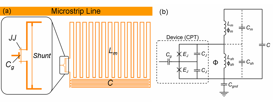
The schematics of the tested circuit is shown in Fig.1. The CPT is inductively coupled via a narrow Al wire (“shunt”) to a lumped-element LC resonator. The LC resonator consists of a meandered 2-μm-wide Al wire with nH and an interdigitated capacitor (2-μm-wide fingers with 2 μm spacing between them) with fF. It was designed to be strongly coupled to the microstrip line in order to increase the signal-to-noise ratio in the low-microwave-power measurements with the average photon occupancy of the resonator . The typical values of the internal and loaded quality factors for these resonators (not coupled to the CPT) were 50,000 and 20,000, respectively. High Q values enable sensitive measurements of small changes in the microwave impedance of the tested device induced by the variations of and . Outside of its bandwidth, the resonator efficiently decouples the CPT from external noises. An additional protection of the CPT from external noises is provided by the shunt: the kinetic inductance of this superconducting wire, nH, is more than 10 times smaller than the effective Josephson inductance of the CPT, which significantly reduces the phase fluctuations across the CPT. The LC resonator was inductively coupled to a 2-port Al microstrip line with a 50 Ω wave impedance. The gate electrode of the CPT is coupled to the central island of the CPT through a capacitor fF.
The sample was mounted inside an -tight copper box which provided the ground plane for the microstrip line and LC resonator. This box was housed inside another -tight copper box in order to attenuate stray photons which may originate from warmer stages of the cryostat Barends et al. (2011). This nested-box construction was anchored to the mixing chamber of a cryogen-free dilution refrigerator at a base temperature of 20 mK.
II.2 Device Fabrication
The Cooper-pair transistor, the lumped-element LC resonator, and the microstrip line were fabricated within the same vacuum cycle using multi-angle electron-beam deposition of Al films through a nanoscale lift-off mask. To minimize the spread of the junction parameters, we have adopted the so-called “Manhattan-pattern” bi-layer lift-off mask formed by a 400-nm-thick e-beam resist (the top layer) and 50-nm-thick copolymer (the bottom layer) (see, e.g., Dolan (1977); Born et al. (2001) and references therein). In this technique, Josephson junctions are formed between the aluminum strips of a well-controlled width overlapping at a right angle. After depositing the photoresist on an undoped Si substrate and its patterning with e-beam lithography, the sample was placed in an ozone asher to remove any traces of the photoresist residue. This step is crucial for reducing the spread in junction parameters. The substrate was then placed in an oil-free high-vacuum chamber with a base pressure of Torr. The axis of the rotatable substrate holder forms an angle of with the direction of e-gun deposition of Al. During the first Al deposition, the substrate holder was positioned such that only the “avenues” were covered with metal; no metal was deposited in the “streets” because the mask thickness is greater than the width of the “streets”. Since the mask thickness is , this technique is suitable for the fabrication of JJs with lateral dimensions up to . The thickness of this first Al film, which forms the central island of the CPT, was 20 nm. Without breaking vacuum, the surface of the bottom electrodes was oxidized at 100 mTorr of dry oxygen for 5 minutes. After evacuating oxygen, the substrate holder was rotated by , and 60-nm-thick top electrodes were deposited along the “streets” (no aluminum is deposited in the “avenues” at this stage). The central island of the Cooper-pair transistor was always deposited during the first Al deposition, and its thickness was smaller than that of the leads; this is important for preventing the quasiparticle poisoning Aumentado et al. (2004). Finally, the sample was removed from the vacuum chamber and the lift-off mask was dissolved in the resist remover. The spread of the resistances for the nominally identical JJs with an area of did not exceed 10%. More than 10 devices with have been studied and the results have been successfully fitted with the numerical simulations; below we discuss two representative samples.
II.3 Measurement Technique
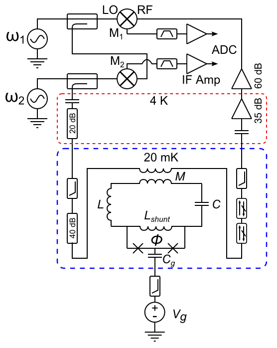
The microwave response of the coupled system “ CPT + LC resonator” was probed by measuring the amplitude and phase of the microwaves traveling along a microstrip line coupled to the resonator. Figure 2 shows a simplified schematic of the microwave circuit, which is similar to the one used in work Manucharyan et al. (2009). The cold attenuators and low-pass filters in the input microwave line prevented leakage of thermal radiation into the resonator. On the output line, a combination of low-pass filters and two cryogenic Pamtech isolators (~18 dB isolation between 3 and 12 GHz) anchored to the mixing chamber were used to attenuate the 5 K noise from the cryogenic amplifier. The DC line for the gate voltage control was heavily filtered with a combination of room temperature LC and low temperature RC filters, followed by a stainless steel powder filter, and a 1:1000 voltage divider.
The probe signal at frequency , generated by a microwave synthesizer (Anritsu MG3694B), was coupled to the cryostat input line through a 16 dB coupler. This signal, after passing the sample, was amplified by a cryogenic HEMT amplifier (Caltech CITCRYO 1-12, 35 dB gain between 1 and 12 GHz) and two 30 dB room-temperature amplifiers. The amplified signal was mixed by mixer M1 with the local oscillator signal at frequency , generated by another synthesizer (Gigatronics 910). The intermediate-frequency signal at MHz was digitized by a GS/s digitizing card (AlazarTech ATS9870). The signal was digitally multiplied by and , averaged over many (typically, ) periods, and its amplitude (proportional to the microwave amplitude ) and phase were extracted as and , respectively (here stands for the time averaging over integer number of periods). The value of randomly changes when both and are varied. To eliminate these random variations, we have also measured the phase of the reference signal provided by mixer M2 and digitized by the second channel of the ADC. The phase difference , being dependent at fixed and only on the electric length difference between the microwave lines inside and outside of the cryostat, is immune to the phase jitter between the two synthesizers. The low noise of this setup allowed us to perform measurements at microwave excitation level down to -140 dBm which corresponded to sub-single-photon population of the tank circuit.
III Model Hamiltonian and Numerical Simulations
We begin with the discussion of the theoretical model of a more general circuit which contains an arbitrary Josephson device coupled via a superconducting “shunt” to a microwave resonator. The only limitation on the device parameters is that all characteristic energies of the device are much smaller than the effective inductive energies of all superconducting wires in the circuit, . The resonance frequency of the circuit might be of the same order or even very close to the device excitation energies, which would lead to the level repulsion. To simplify the notations, we shall use below the units (e.g., in these units ) and restore the physical units at the end, where we apply this model to the specific case of a device that consists of two Josephson junctions and one superconducting island, i.e. the CPT.
The generalized circuit shown in Fig. 1b includes two loops: the long meandering wire, the shunt, and a large capacitor form one loop (referred below as the “resonator” loop), and the device and the shunt form another loop (referred as the “device” loop). The inductance of the meander (shunt), and the phase difference across this element are () and (), respectively. The difference between the device phase and the shunt phase is due to the time-independent magnetic flux in the device loop: , where , is the flux quantum. The voltage drops across the device and the shunt are equal: . The whole circuit is described by the Lagrangian
Here () is the time-dependent part (i.e. the kinetic energy) of the response of the meander (shunt), and is the device Lagrangian which also depends on the internal degrees of freedom (phases) of the device. In the BCS theory, the response of a superconducting wire with the static energy has a scale of at all frequencies ; it is a function of the dimensionless parameter : where is the superconducting gap. This equation implies that at low frequencies, the wire impedance acquires, in addition to the kinetic inductance, a small capacitive component (these capacitances are shown in Fig. 1b by dashed lines).
We shall assume that the device Lagrangian is given by the sum of the Josephson and electrostatic energies:
| (2) |
Here phases and corresponding potentials describe both the internal degrees of freedom of the device and the shunt phase.
Because the potential energy of the resonator loop is much greater than that of the device, the effect of the device on this loop can be treated as a small perturbation. In the absence of the device, the resonator loop has two modes: the harmonic oscillation of the total phase with frequency where , , and the orthogonal mode with . Because the large capacitance does not participate in the second mode, the frequency of this mode is determined by the superconducting gap, the only energy scale in this case. We shall assume that so both real and virtual excitations of this mode can be neglected as well as the contribution of the capacitances and to the effective capacitance of the first mode. Note, however, that the virtual processes involving the second mode are small only in and might not be completely negligible in a realistic situation. If these processes are neglected, there is only one relevant degree of freedom, the phase across the device . The effective Lagrangian is reduced to
| (3) |
with and
| (4) |
Fluctuations of the phase in the low-energy states of the oscillator mode are very small:
where is the quantum number of the oscillator states. This allows one to replace the solution of the full problem by the solution of the simplified model in which we expand the interaction term in small phase fluctuations.
It will be more convenient to use the Hamiltonian formalism in which the conjugated degrees of freedom are phases and charges. The total Hamiltonian is the sum of three parts, the Hamiltonians of the resonator (), device ( and interaction between them () :
| (5) | |||||
| (6) | |||||
| (7) |
The coupling to the inductor charge fluctuations contains the inverse of the capacitance matrix () and thus is very small. Thus, even though the charge fluctuations across the shunt are not small:
their effect on the coupling can be treated perturbatively. In the leading order in the interaction, we need to keep only two types of terms. The first type is quadratic in phase and diagonal in the basis of resonator states. The second type is linear in and off diagonal in this basis. The quadratic terms in the inductor charge are absent, so the charge coupling appears only due to the off diagonal terms that are linear in . The Hamiltonian equivalent to (3) becomes
| (8) |
Here () is the creation (annihilation) operator for the harmonic oscillations of the circuit, and are operators acting on the device which forms are obtained by expanding the interaction Hamiltonian
| (9) | |||||
| (10) | |||||
| (11) |
We now estimate the scale of the frequency deviations induced by these perturbations. In the natural units of the resonator frequency , the scales of the perturbing operators are , and . The operator is diagonal in the oscillator states, so it directly results in the frequency shift Because the non-diagonal elements affect the level of the resonator only in the second order of the perturbation theory, the effect of the and operators depends on the gap between the levels in the combined resonator/device circuit. Far away from the full frustration and charge degeneracy point (, ), the device is characterized by large and the energy levels are separated by large gaps, so the smallest gap is due to the resonator: . In this case the frequency shifts are and respectively, which implies . The effect induced by the phase and charge coupling grows when the gap between the levels coupled by these operators becomes small, but the phase coupling remains larger than the charge coupling for the devices with This increase of the frequency shift occurs, for instance, when the device level crosses the first resonator level.
We now write down the explicit equations for the Cooper pair box. In this case, the internal degrees of freedom are limited to one phase (and the conjugated charge). Assuming equal capacitances and Josephson energies of the CPT junctions, we have
| (12) | |||||
| (13) | |||||
| (14) | |||||
| (15) |
Here we restored the physical energy units . For practical computations it is sufficient to retain the first few levels of the resonator ( and some number, , of the charging states. The Hamiltonian (8) becomes matrix. Because the wave function of the charge decreases exponentially at large charges, , it is sufficient to consider for accurate computations. The straightforward numerical digonalization of the Hamiltonian (8) leads to the theoretical predictions that can be compared with the data.
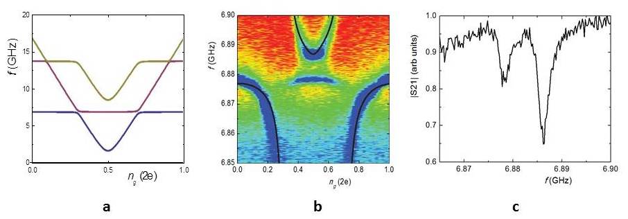
Our experimental situation corresponds to and . In the absence of frustrations, the frequency of the lowest CPT level is very high: . The frequency of the lowest CPT level decreases as the magnetic field frustrates the Josephson coupling and/or with approaching the charge degeneracy (. Figure 3a shows three low-energy levels of the system “CPT+resonator” with the parameters typical for our experiment. Note that for the studied circuits, only the combined effect of flux- and charge-induced frustrations brings the frequency of the first device level below that of the resonator, otherwise the device resonance frequency significantly exceeds that of the resonator even at full flux frustration (e.g. at ).
IV Experimental Results and Discussion
Below we present the measurements of the amplitude of the transmitted microwaves (unless otherwise specified) at the base temperature mK. Most of the data (with the exception of the data in Fig.3b,c) are shown for only one representative device. The resonant dependence of on the microwave frequency , measured for this device at and , is shown in the inset to Fig. 4. The resonance frequency depends periodically on and ; for example, the dependence measured at is shown in Figure 4. The period in charge is at the base temperature (see Fig.5); it changes from to at higher temperatures (>300 mK) due to the presence of thermally excited quasiparticles. Note that the total time of acquisition for the data shown in Fig.3b was approximately 20 minutes; over longer time intervals, the periodicity of might be disrupted by the motion of non-equilibrium quasiparticles to/from the CPT island (the so-called “quasiparticle poisoning”) Aumentado et al. (2004) or other types of charge fluctuations Faoro and Ioffe (2006). The high stability of the charge on the CPT island indicates that (a) the combination of a larger superconducting gap of the CPT island and its relatively large charging energy protects the CPT from quasiparticle poisoning, and (b) the double-wall -tight sample box shields the device from stray high-energy photons. The microwave photon energy GHz is insufficiently large to excite the CPT at : indeed, according to our simulations, the lowest excitation frequency for this device exceeds 30 GHz even at full flux frustration (). In this case the variation of the resonance frequency with magnetic flux reflects the -dependence of the CPT impedance in its ground state.
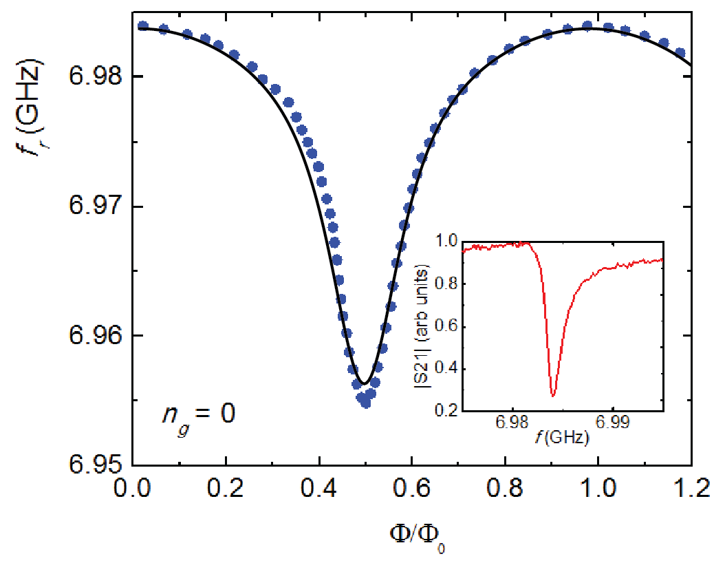
The dependences of the resonance frequency on are illustrated by Figs. 5(a-e), where the color-coded microwave amplitude is plotted versus and for several values of the magnetic flux in the device loop. The black curves in Fig. 5 show the results of fitting the experimental data with our numerical simulations. All these curves were generated with the same set of fitting parameters: GHz, GHz and GHz (note that not only the amplitude of the resonance frequency modulation, but also the absolute values of are pre-determined by these parameters). The fitting procedure is very sensitive to the choice of these parameters: we believe that they are determined with an accuracy better than 10%. The extracted charging energy coincides (within 5% accuracy) with an estimate of based on the junction area, the specific geometrical capacitance for Al tunnel junctions ( fF/, see e.g,. Delsing et al. (1994)), and the electronic capacitance of Josephson junctions, (0.3 fF at kΩ) Larkin and Ovchinnikov (1983); Eckern et al. (1984). The Josephson energy estimated on the basis of the Ambegaokar-Baratoff relationship Tinkham (1996) using the normal-state resistance of a test junction deposited on the same chip is ~40% greater than the fit value of .
Generally, one expects that Josephson circuits can be accurately described by the Hamiltonian consisting of Josephson and charging energies (cf. Eq.2) only if all energy scales are smaller than . Away from full frustration, the energy of the CPT excited state is of the order of Josephson plasma frequency K, which is comparable to . Thus, the excellent agreement between the experimental data and numerical modeling, observed over the whole range of and , is quite surprising.
It is worth noting that the circuit modeling based on the numerical diagonalization of the circuit Hamiltonian is essential for fitting the data for devices with . For example, the analytical solution for the Josephson inductance in the CPT ground state, calculated within the two-level approximation (Eq. 4 in Ref. Paila et al. (2009)), overestimates the amplitude of the dependence at small flux frustrations by almost an order of magnitude. The latter solution provides more accurate fitting of the experiment at larger frustrations (), but becomes inadequate again at when the avoided level crossing is observed.
The evolution of these dependences reflects the modification of the CPT spectrum with and . For a small phase difference (Figs.5a-b), the lowest CPT excitation frequency well exceeds the microwave frequency (which is close to the resonance frequency of the resonator), and the CPT remains in its ground state for all including the charge degeneracy point (). In this regime, the dependences mostly reflect the variations of the CPT impedance with in the CPT ground state. At a larger frustration (Fig. 5c), the lowest CPT level approaches the lowest resonator level (but has not crossed it yet), and the entanglement of the qubit and resonator states leads to a complicated shape of the dependence. Finally, with the further approach to full frustration (, Figs. 5d,e), the CPT excitation frequency becomes smaller than the resonance frequency of the LC resonator, and the shape of the dependences abruptly changes: they are strongly affected by the avoided level crossing. The plots in this regime consist of two sets of curves. The lower set of curves corresponds to the lowest energy level of the combined system “CPT + resonator” (this level coincides with the CPT lowest level when approaching the charge degeneracy points, i.e. far away from the resonance frequency of the resonator). The upper set of curves corresponds to the first excited level of the system “CPT + resonator”: with approaching the charge degeneracy point, this level descends from higher energies to its lowest position at . The visibility of the upper set of curves depends on the proximity between the CPT and resonator levels. Indeed, if the energy of the CPT resonance at is much lower than the first resonator level, the upper-curve “cone” is very sharp, and the corresponding microwave resonance is smeared even for small deviations of from (this case is illustrated by Figs. 5d,e). On the other hand, the “cone” becomes broader when the intersecting CPT and resonator levels are close to one another: in this case illustrated by Fig. 1b, we were able to follow the upper set of curves over the frequency range of ~15 MHz.
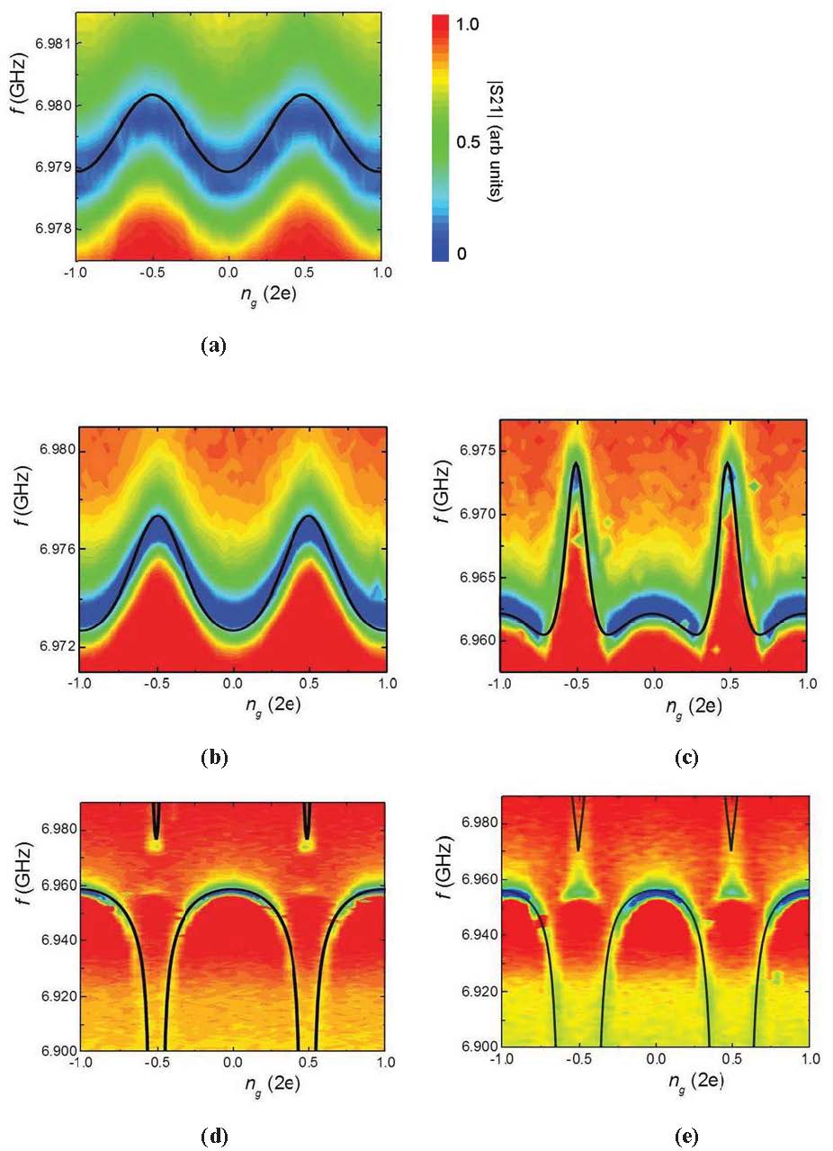
For both devices, whose dependences are shown in Figs. 3 and 5, we observed a double-resonance structure at full frustration and charge degeneracy, depicted in Figs. 3b,c and 5e. The second (low-frequency) resonance appears as a “shadow” of the resonance observed at . The appearance of this resonance, much weaker than that at , implies that there are fluctuations of the island offset charge which are fast at the measuring time scale ~0.1 s. These fluctuations change the effective from 0.5 to 0. We attribute these fluctuations to the non-equilibrium quasiparticles moving between the CPT island and the leads. At , the energy of a quasiparticle on the island exceeds the energy of quasiparticles in the leads by . Here is the difference between superconducting gaps in the island and the leads due to the difference in the thicknesses of these Al films; we estimate to be ~. In our devices, the probability of these fluctuations is small (the amplitude of the resonance is much greater than that of its “shadow” at ), which suggests that the quantity remains positive (albeit small) at .
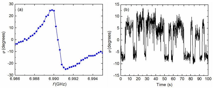
The sensitivity of the studied circuit to the charge on the CPT island is illustrated by Fig.6. Figure 6b shows the time dependence of the phase of transmitted microwaves when the microwave frequency is tuned to the resonance of the “CPT + resonator” circuit. The noise was measured at full flux frustration () when an avoided crossing between the CPT and resonator levels was observed, but relatively far from the charge degeneracy point (). The amplitude of the observed telegraph noise corresponds to the charge fluctuations due to, presumably, coupling of the CPT island to a single charge fluctuator in its environment.
V Conclusions.
We have performed a detailed analysis of the microwave response of Cooper pair transistors with coupled to a lumped element resonator as a function of the magnetic flux and the gate voltage. Away from the full frustration in flux and charge the levels of the Cooper pair transistor are far away from the resonator frequency. In this regime the modulation of the resonator frequency induced by CPT can be described as the effective inductance of the CPT that adds to the inductance of the resonator. Close to the full frustration the frequency of the resonator approaches and eventually crosses the excitation level of the Cooper pair transistor resulting in a complex pattern of the resonator frequency dependence on the flux and gate voltage. In all regimes the resonator frequency dependence is very well described by the results of the numerical diagonalization of the full Hamiltonian that contains the resonator and CPT. High sensitivity of the resonator frequency close to the level crossing provides the tool to measure charge fluctuations in the environment with high accuracy and short time resolution.
We would like to thank J. Aumentado and V. Manucharyan for helpful discussions. We acknowledge the support from the DARPA (under grant HR0011-09-1-0009), ARO (W911NF-09-1-0395), and NSF (NIRT ECS-0608842).
References
- Averin and Likharev (1991) D. Averin and K. Likharev, in Mesoscopic Phenomena in Solids, edited by B. Altshuler, P. Lee, and R. A. Webb (North-Holland, Amsterdam, 1991), p. 173.
- Aumentado (2010) J. Aumentado, in The Handbook of Nanophysics (Taylor and Francis, New York, 2010), p. 779.
- Duty et al. (2005) T. Duty, G. Johansson, K. Bladh, D. Gunnarsson, C. Wilson, and P. Delsing, Physical Review Letters 95, 206807 (2005), ISSN 0031-9007, URL http://dx.doi.org/10.1103/PhysRevLett.95.206807.
- Naaman and Aumentado (2006) O. Naaman and J. Aumentado, Physical Review B (Condensed Matter and Materials Physics) 73, 172504 (2006), ISSN 0163-1829, URL http://dx.doi.org/10.1103/PhysRevB.73.172504.
- Nakamura et al. (1999) Y. Nakamura, Y. Pashkin, and J. Tsai, Nature 398, 786 (1999), ISSN 0028-0836, URL http://dx.doi.org/10.1038/19718.
- Vion et al. (2002) D. Vion, A. Aassime, A. Cottet, P. Joyez, H. Pothier, C. Urbina, D. Esteve, and M. Devoret, Science 296, 886 (2002), ISSN 0036-8075, URL http://dx.doi.org/10.1126/science.1069372.
- Wallraff et al. (2005) A. Wallraff, D. Schuster, A. Blais, L. Frunzio, J. Majer, M. Devoret, S. Girvin, and R. Schoelkopf, Physical Review Letters 95, 060501 (2005), ISSN 0031-9007, URL http://dx.doi.org/10.1103/PhysRevLett.95.060501.
- Paila et al. (2009) A. Paila, D. Gunnarsson, J. Sarkar, M. Sillanpaa, and P. Hakonen, Physical Review B (Condensed Matter and Materials Physics) 80, 144520 (2009), ISSN 1098-0121, URL http://dx.doi.org/10.1103/PhysRevB.80.144520.
- Widom et al. (1984) A. Widom, G. Megaloudis, T. Clark, J. Mutton, R. Prance, and H. Prance, Journal of Low Temperature Physics 57, 651 (1984), ISSN 0022-2291.
- Averin et al. (1985) D. Averin, A. Zorin, and K. Likharev, Soviet Physics - JETP 61, 407 (1985), ISSN 0038-5646.
- Sillanpaa et al. (2005) M. Sillanpaa, T. Lehtinen, A. Paila, Y. Makhlin, L. Roschier, and P. Hakonen, Physical Review Letters 95, 206806 (2005), ISSN 0031-9007, URL http://dx.doi.org/10.1103/PhysRevLett.95.206806.
- Doucot and Ioffe (2007) B. Doucot and L. Ioffe, Physical Review B (Condensed Matter and Materials Physics) 76, 214507 (2007), ISSN 1098-0121, URL http://dx.doi.org/10.1103/PhysRevB.76.214507.
- Gladchenko et al. (2009) S. Gladchenko, D. Olaya, E. Dupont-Ferrier, B. Doucot, L. B. Ioffe, and M. E. Gershenson, Nature Physics 5, 48 (2009), URL http://dx.doi.org/10.1038/nphys1151.
- Barends et al. (2011) R. Barends, J. Wenner, M. Lenander, Y. Chen, R. C. Bialczak, J. Kelly, E. Lucero, P. O Malley, M. Mariantoni, D. Sank, et al., Appl.Phys.Lett. 99, 113507 (2011), ISSN 00036951, URL http://dx.doi.org/10.1063/1.3638063.
- Dolan (1977) G. Dolan, Applied Physics Letters 31, 337 (1977), ISSN 0003-6951, URL http://dx.doi.org/10.1063/1.89690.
- Born et al. (2001) D. Born, T. Wagner, W. Krech, U. Hubner, and L. Fritzsch, IEEE Transactions on Applied Superconductivity 11, 373 (2001), ISSN 1051-8223, URL http://dx.doi.org/10.1109/77.919360.
- Aumentado et al. (2004) J. Aumentado, M. Keller, J. Martinis, and M. Devoret, Physical Review Letters 92, 066802 (2004), ISSN 0031-9007, URL http://dx.doi.org/10.1103/PhysRevLett.92.066802.
- Manucharyan et al. (2009) V. Manucharyan, J. Koch, L. Glazman, and M. Devoret, Science 326, 113 (2009), ISSN 0036-8075, URL http://dx.doi.org/10.1126/science.1175552.
- Faoro and Ioffe (2006) L. Faoro and L. Ioffe, Physical Review Letters 96, 047001 (2006), ISSN 0031-9007, URL http://dx.doi.org/10.1103/PhysRevLett.96.047001.
- Delsing et al. (1994) P. Delsing, C. Chen, D. Haviland, Y. Harada, and T. Claeson, Physical Review B (Condensed Matter) 50, 3959 (1994), ISSN 0163-1829, URL http://dx.doi.org/10.1103/PhysRevB.50.3959.
- Larkin and Ovchinnikov (1983) A. Larkin and Y. Ovchinnikov, Physical Review B (Condensed Matter) 28, 6281 (1983), ISSN 0163-1829, URL http://dx.doi.org/10.1103/PhysRevB.28.6281.
- Eckern et al. (1984) U. Eckern, G. Schon, and V. Ambegaokar, Physical Review B (Condensed Matter) 30, 6419 (1984), ISSN 0163-1829, URL http://dx.doi.org/10.1103/PhysRevB.30.6419.
- Tinkham (1996) M. Tinkham, Introduction to superconductivity (McGraw-Hill Book Co, New York, 1996).